Document Outline
- General Description
- Features
- Block Diagram
- Pin Assignment
- Pin Descriptions
- Pin Characteristics
- Control Input Function Table
- Absolute Maximum Ratings
- Power Supply 3.3V DC Characteristics
- Power Supply 3.3V/2.5V DC Characteristics
- Power Supply 2.5V DC Characteristics
- LVCMOS DC Characteristics
- Differential DC Characteristics
- LVPECL DC Characteristics
- 3.3V AC Characteristics
- 3.3V/2.5V AC Characteristics
- 2.5V AC Characteristics
- Typical Phase Noise Plot
- Parameter Measurement Information
- Application Information
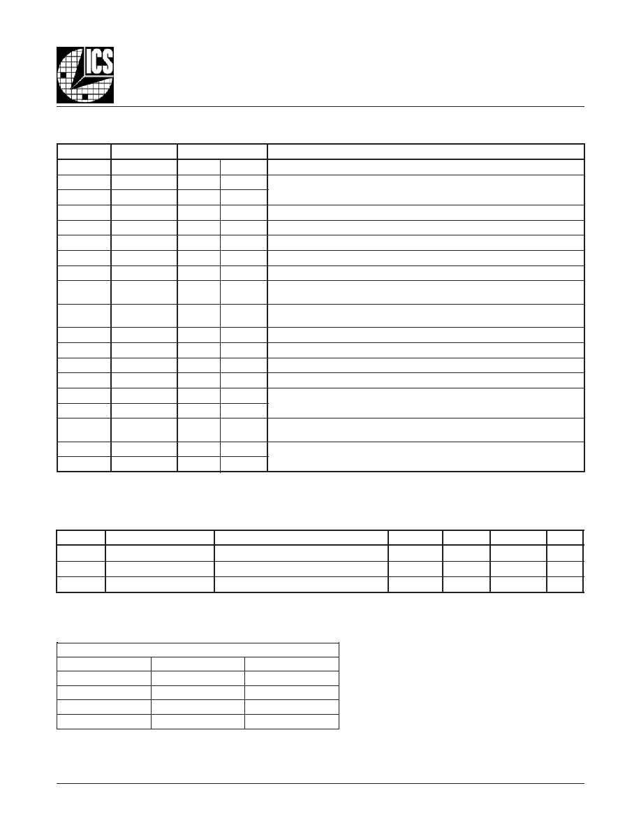
- Power Supply Filtering Techniques
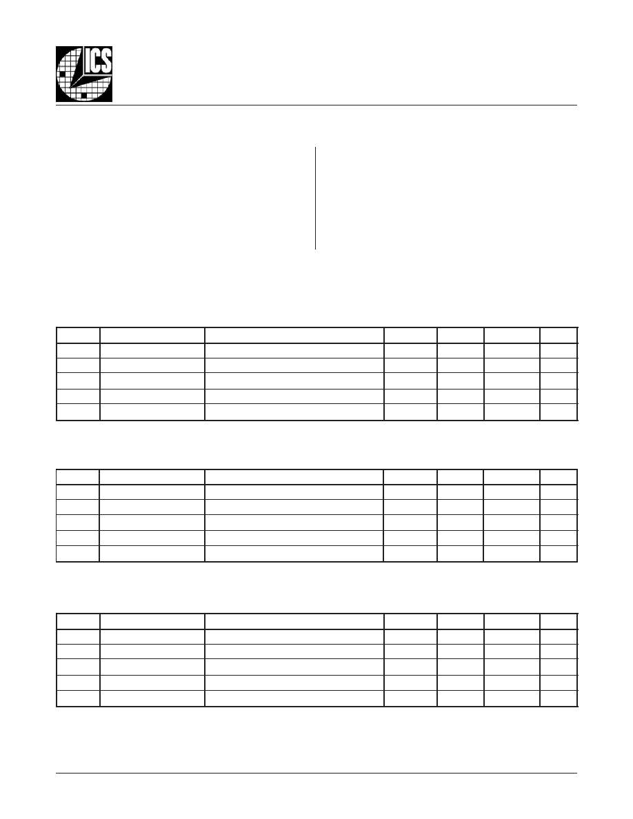
- Wiring the Differential Input to Accept Single Ended Levels
- VCXO Crystal Selection
- Example Crystal Parameters
- Varactor Parameters
- Formulas
- Example Calculations
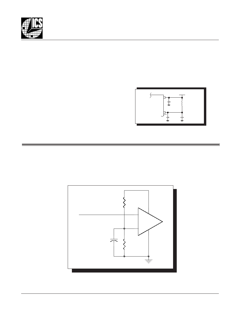
- Differential Clock Input Interface
- Recommendations for Unused Input and Output Pins
- Termination for 3.3V LVPECL Output
- Termination for 2.5V LVPECL Output
- Power Considerations
- Power Dissipation
- Junction Temperature
- Thermal Resistance
- Calculations & Equations
- LVPECL Driver Circuit & Termination
- Reliability Information
- Transistor Count
- Package Outline
- Package Dimensions
- Ordering Information

813001AGI
www.icst.com/products/hiperclocks.html
REV. A SEPTEMBER 2, 2005
1
Integrated
Circuit
Systems, Inc.
ICS813001I
D
UAL
VCXO
W
/3.3V, 2.5V LVPECL
F
EMTO
C
LOCK
TM PLL
G
ENERAL
D
ESCRIPTION
The ICS813001I is a dual VCXO + FemtoClockTM
Multiplier designed for use in Discrete PLL
loops. Two selectable external VCXO crystals
allow the device to be used in multi-rate appli-
cations, where a given line card can be
switched, for example, between 1Gb Ethernet (125MHz
s y s t e m r e f e r e n c e c l o c k ) a n d 1 G b F i b r e C h a n n e l
(106.25MHz system reference clock) modes. Of course,
a multitude of other applications are also possible such
as switching between 74.25MHz and 74.175824MHz
for HDTV, switching between SONET, FEC and non FEC
rates, etc.
The ICS813001I is a two stage device � a VCXO followed
by a FemtoClock PLL. The FemtoClock PLL can multiply
the crystal frequency of the VCXO to provide an output
frequency range of 40.83MHz to 640MHz, with a random
rms phase jitter of less than 1ps (12kHz � 20MHz). This
phase jitter performance meets the requirements of 1Gb/
10Gb Ethernet, 1Gb, 2Gb, 4Gb and 10Gb Fibre Channel,
and SONET up to OC48. The FemtoClock PLL can also be
bypassed if frequency multiplication is not required. For
testing/debug purposes, de-assertion of the output enable
pin will place both Q and nQ in a high impedance state.
F
EATURES
� One 3.3V or 2.5V LVPECL output pair
� Two selectable crystal oscillator interfaces for the VCXO,
one differential clock or one LVCMOS/LVTTL clock inputs
� CLK1/nCLK1 supports the following input types:
LVPECL, LVDS, LVHSTL, SSTL, HCSL
� Crystal operating frequency range: 14MHz - 24MHz
� VCO range: 490MHz - 640MHz
� Output frequency range: 40.83MHz - 640MHz
� VCXO pull range: �100ppm (typical)
� Supports the following applications (among others):
SONET, Ethernet, Fibre Channel, HDTV, MPEG
� RMS phase jitter @ 622.08MHz (12kHz - 20MHz):
0.84 (typical)
� Supply voltage modes:
V
CC
/V
CCO
3.3V/3.3V
3.3V/2.5V
2.5V/2.5V
� -40�C to 85�C ambient operating temperature
� Available in both, Standard and RoHS/Lead-Free
compliant packages
HiPerClockSTM
ICS
B
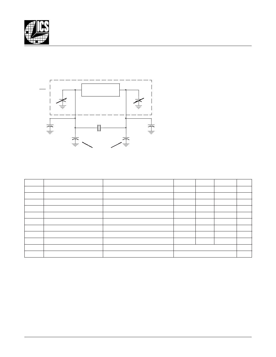
LOCK
D
IAGRAM
VCXO
1 0
(default)
1 1
0 0
0 1
PD
VCO
490-640MHz
0
1
Feedback Divider M
Output Divider N
M2:M0
000 �16
001 �20
010 �22
011 �24
100 �25
(default)
101 �32
110 �40
111 MR
N2:N0
000 �1
001 �2
010 �3
011 �4
(default)
100 �5
101 �6
110 �8
111 �12
P
IN
A
SSIGNMENT
ICS813001I
24-Lead TSSOP
4.40mm x 7.8mm x 0.92mm
package body
G Package
Top View
VCO_SEL
N 0
N 1
N 2
V
CCO
Q
nQ
V
EE
V
CCA
V
CC
XTAL_OUT1
XTAL_IN1
1
2
3
4
5
6
7
8
9
10
11
12
CLK_SEL1
CLK_SEL0
OE
M2
M1
M0
CLK1
nCLK1
CLK0
VC
XTAL_IN0
XTAL_OUT0
24
23
22
21
20
19
18
17
16
15
14
13
VCO_SEL
CLK_SEL0
CLK_SEL1
CLK0
CLK1
nCLK1
VC
M2
M1
M0
N2
N1
N0
O E
Pullup
Pullup
Pullup
Q
nQ
XTAL_IN0
XTAL_OUT0
XTAL_IN1
XTAL_OUT1
Pulldown
Pulldown
Pullup
Pullup
Pullup
Pullup
Pulldown
Pulldown
Pulldown
Pulldown
813001AGI
www.icst.com/products/hiperclocks.html
REV. A SEPTEMBER 2, 2005
2
Integrated
Circuit
Systems, Inc.
ICS813001I
D
UAL
VCXO
W
/3.3V, 2.5V LVPECL
F
EMTO
C
LOCK
TM PLL
T
ABLE
1. P
IN
D
ESCRIPTIONS
T
ABLE
2. P
IN
C
HARACTERISTICS
l
o
b
m
y
S
r
e
t
e
m
a
r
a
P
s
n
o
i
t
i
d
n
o
C
t
s
e
T
m
u
m
i
n
i
M
l
a
c
i
p
y
T
m
u
m
i
x
a
M
s
t
i
n
U
C
N
I
e
c
n
a
t
i
c
a
p
a
C
t
u
p
n
I
4
F
p
R
N
W
O
D
L
L
U
P
r
o
t
s
i
s
e
R
n
w
o
d
ll
u
P
t
u
p
n
I
1
5
k
R
P
U
L
L
U
P
r
o
t
s
i
s
e
R
p
u
ll
u
P
t
u
p
n
I
1
5
k
1
L
E
S
_
O
C
V
t
u
p
n
I
p
u
ll
u
P
.
s
l
e
v
e
l
e
c
a
f
r
e
t
n
i
L
T
T
V
L
/
S
O
M
C
V
L
.
n
i
p
t
c
e
l
e
s
O
C
V
3
,
2
1
N
,
0
N
t
u
p
n
I
p
u
ll
u
P
.
4
�
=
e
u
l
a
v
t
l
u
a
f
e
D
.
s
n
i
p
t
c
e
l
e
s
r
e
d
i
v
i
d
t
u
p
t
u
O
.
s
l
e
v
e
l
e
c
a
f
r
e
t
n
i
L
T
T
V
L
/
S
O
M
C
V
L
4
2
N
t
u
p
n
I
n
w
o
d
ll
u
P
5
V
O
C
C
r
e
w
o
P
.
n
i
p
y
l
p
p
u
s
t
u
p
t
u
O
7
,
6
Q
n
,
Q
t
u
p
u
O
.
s
l
e
v
e
l
e
c
a
f
r
e
t
n
i
L
C
E
P
V
L
.
r
i
a
p
t
u
p
t
u
o
l
a
i
t
n
e
r
e
f
f
i
D
8
V
E
E
r
e
w
o
P
.
n
i
p
y
l
p
p
u
s
e
v
i
t
a
g
e
N
9
V
A
C
C
r
e
w
o
P
.
n
i
p
y
l
p
p
u
s
g
o
l
a
n
A
0
1
V
C
C
r
e
w
o
P
.
n
i
p
y
l
p
p
u
s
e
r
o
C
1
1
2
1
,
1
T
U
O
_
L
A
T
X
1
N
I
_
L
A
T
X
t
u
p
n
I
,
t
u
p
t
u
o
e
h
t
s
i
1
T
U
O
_
L
A
T
X
.
e
c
a
f
r
e
t
n
i
l
a
t
s
y
r
c
t
n
a
n
o
s
e
r
l
e
ll
a
r
a
P
.
t
u
p
n
i
e
h
t
s
i
1
N
I
_
L
A
T
X
3
1
4
1
,
0
T
U
O
_
L
A
T
X
0
N
I
_
L
A
T
X
t
u
p
n
I
,
t
u
p
t
u
o
e
h
t
s
i
0
T
U
O
_
L
A
T
X
.
e
c
a
f
r
e
t
n
i
l
a
t
s
y
r
c
t
n
a
n
o
s
e
r
l
e
ll
a
r
a
P
.
t
u
p
n
i
e
h
t
s
i
0
N
I
_
L
A
T
X
5
1
C
V
t
u
p
n
I
.
t
u
p
n
i
e
g
a
t
l
o
v
l
o
r
t
n
o
c
O
X
C
V
6
1
0
K
L
C
t
u
p
n
I
n
w
o
d
ll
u
P
.
t
u
p
n
i
k
c
o
l
c
L
T
T
V
L
/
S
O
M
C
V
L
7
1
1
K
L
C
n
t
u
p
n
I
p
u
ll
u
P
.
t
u
p
n
i
k
c
o
l
c
l
a
i
t
n
e
r
e
f
f
i
d
g
n
i
t
r
e
v
n
I
8
1
1
K
L
C
t
u
p
n
I
n
w
o
d
ll
u
P
.
t
u
p
n
i
k
c
o
l
c
l
a
i
t
n
e
r
e
f
f
i
d
g
n
i
t
r
e
v
n
i
-
n
o
N
0
2
,
9
1
1
M
,
0
M
t
u
p
n
I
n
w
o
d
ll
u
P
.
5
2
�
=
e
u
l
a
v
t
l
u
a
f
e
D
.
s
n
i
p
t
c
e
l
e
s
r
e
d
i
v
i
d
k
c
a
b
d
e
e
F
.
s
l
e
v
e
l
e
c
a
f
r
e
t
n
i
L
T
T
V
L
/
S
O
M
C
V
L
1
2
2
M
t
u
p
n
I
p
u
ll
u
P
2
2
E
O
t
u
p
n
I
p
u
ll
u
P
t
u
p
t
u
o
e
h
t
,
W
O
L
n
e
h
W
.
e
v
i
t
c
a
s
i
t
u
p
t
u
o
e
h
t
,
H
G
I
H
n
e
h
W
.
e
l
b
a
n
e
t
u
p
t
u
O
.
s
l
e
v
e
l
e
c
a
f
r
e
t
n
i
L
T
T
V
L
/
S
O
M
C
V
L
.
e
t
a
t
s
e
c
n
a
d
e
p
m
i
h
g
i
h
a
n
i
s
i
3
2
0
L
E
S
_
K
L
C
t
u
p
n
I
n
w
o
d
ll
u
P
.
3
e
l
b
a
T
o
t
r
e
f
e
R
.
s
l
e
v
e
l
e
c
a
f
r
e
t
n
i
L
T
T
V
L
/
S
O
M
C
V
L
.
n
i
p
t
c
e
l
e
s
k
c
o
l
C
4
2
1
L
E
S
_
K
L
C
t
u
p
n
I
p
u
ll
u
P
:
E
T
O
N
p
u
ll
u
P
d
n
a
n
w
o
d
ll
u
P
.
s
e
u
l
a
v
l
a
c
i
p
y
t
r
o
f
,
s
c
i
t
s
i
r
e
t
c
a
r
a
h
C
n
i
P
,
2
e
l
b
a
T
e
e
S
.
s
r
o
t
s
i
s
e
r
t
u
p
n
i
l
a
n
r
e
t
n
i
o
t
r
e
f
e
r
T
ABLE
3. C
ONTROL
I
NPUT
F
UNCTION
T
ABLE
s
t
u
p
n
I
1
L
E
S
_
K
L
C
0
L
E
S
_
K
L
C
t
u
p
n
I
d
e
t
c
e
l
e
S
0
0
0
K
L
C
0
1
1
K
L
C
n
,
1
K
L
C
1
0
0
L
A
T
X
1
1
1
L
A
T
X
813001AGI
www.icst.com/products/hiperclocks.html
REV. A SEPTEMBER 2, 2005
3
Integrated
Circuit
Systems, Inc.
ICS813001I
D
UAL
VCXO
W
/3.3V, 2.5V LVPECL
F
EMTO
C
LOCK
TM PLL
T
ABLE
4A. P
OWER
S
UPPLY
DC C
HARACTERISTICS
,
V
CC
= V
CCA
= V
CCO
= 3.3V�5%, TA = -40�C
TO
85�C
A
BSOLUTE
M
AXIMUM
R
ATINGS
Supply Voltage, V
CC
4.6V
Inputs, V
I
-0.5V to V
CC
+ 0.5V
Outputs, I
O
(LVPECL)
Continuous Current
50mA
Surge Current
100mA
Package Thermal Impedance,
JA
70�C/W (0 lfpm)
Storage Temperature, T
STG
-65�C to 150�C
NOTE: Stresses beyond those listed under Absolute
Maximum Ratings may cause permanent damage to the
device. These ratings are stress specifications only. Functional
operation of product at these conditions or any conditions be-
yond those listed in the
DC Characteristics
or
AC Character-
istics
is not implied. Exposure to absolute maximum rating
conditions for extended periods may affect product reliability.
T
ABLE
4C. P
OWER
S
UPPLY
DC C
HARACTERISTICS
,
V
CC
= V
CCA
= V
CCO
= 2.5V�5%, TA = -40�C
TO
85�C
T
ABLE
4B. P
OWER
S
UPPLY
DC C
HARACTERISTICS
,
V
CC
= V
CCA
= 3.3V�5%, V
CCO
= 2.5V�5%, TA = -40�C
TO
85�C
l
o
b
m
y
S
r
e
t
e
m
a
r
a
P
s
n
o
i
t
i
d
n
o
C
t
s
e
T
m
u
m
i
n
i
M
l
a
c
i
p
y
T
m
u
m
i
x
a
M
s
t
i
n
U
V
C
C
e
g
a
t
l
o
V
y
l
p
p
u
S
e
r
o
C
5
3
1
.
3
3
.
3
5
6
4
.
3
V
V
A
C
C
e
g
a
t
l
o
V
y
l
p
p
u
S
g
o
l
a
n
A
5
3
1
.
3
3
.
3
5
6
4
.
3
V
V
O
C
C
e
g
a
t
l
o
V
y
l
p
p
u
S
t
u
p
t
u
O
5
3
1
.
3
3
.
3
5
6
4
.
3
V
I
E
E
t
n
e
r
r
u
C
y
l
p
p
u
S
r
e
w
o
P
0
3
1
A
m
I
A
C
C
t
n
e
r
r
u
C
y
l
p
p
u
S
g
o
l
a
n
A
0
1
A
m
l
o
b
m
y
S
r
e
t
e
m
a
r
a
P
s
n
o
i
t
i
d
n
o
C
t
s
e
T
m
u
m
i
n
i
M
l
a
c
i
p
y
T
m
u
m
i
x
a
M
s
t
i
n
U
V
C
C
e
g
a
t
l
o
V
y
l
p
p
u
S
e
r
o
C
5
3
1
.
3
3
.
3
5
6
4
.
3
V
V
A
C
C
e
g
a
t
l
o
V
y
l
p
p
u
S
g
o
l
a
n
A
5
3
1
.
3
3
.
3
5
6
4
.
3
V
V
O
C
C
e
g
a
t
l
o
V
y
l
p
p
u
S
t
u
p
t
u
O
5
7
3
.
2
5
.
2
5
2
6
.
2
V
I
E
E
t
n
e
r
r
u
C
y
l
p
p
u
S
r
e
w
o
P
0
3
1
A
m
I
A
C
C
t
n
e
r
r
u
C
y
l
p
p
u
S
g
o
l
a
n
A
0
1
A
m
l
o
b
m
y
S
r
e
t
e
m
a
r
a
P
s
n
o
i
t
i
d
n
o
C
t
s
e
T
m
u
m
i
n
i
M
l
a
c
i
p
y
T
m
u
m
i
x
a
M
s
t
i
n
U
V
C
C
e
g
a
t
l
o
V
y
l
p
p
u
S
e
r
o
C
5
7
3
.
2
5
.
2
5
2
6
.
2
V
V
A
C
C
e
g
a
t
l
o
V
y
l
p
p
u
S
g
o
l
a
n
A
5
7
3
.
2
5
.
2
5
2
6
.
2
V
V
O
C
C
e
g
a
t
l
o
V
y
l
p
p
u
S
t
u
p
t
u
O
5
7
3
.
2
5
.
2
5
2
6
.
2
V
I
E
E
t
n
e
r
r
u
C
y
l
p
p
u
S
r
e
w
o
P
5
2
1
A
m
I
A
C
C
t
n
e
r
r
u
C
y
l
p
p
u
S
g
o
l
a
n
A
0
1
A
m

813001AGI
www.icst.com/products/hiperclocks.html
REV. A SEPTEMBER 2, 2005
4
Integrated
Circuit
Systems, Inc.
ICS813001I
D
UAL
VCXO
W
/3.3V, 2.5V LVPECL
F
EMTO
C
LOCK
TM PLL
T
ABLE
4E. LVPECL DC C
HARACTERISTICS
,
TA = -40�C
TO
85�C
T
ABLE
4C. LVCMOS / LVTTL DC C
HARACTERISTICS
,
TA = -40�C
TO
85�C
l
o
b
m
y
S
r
e
t
e
m
a
r
a
P
s
n
o
i
t
i
d
n
o
C
t
s
e
T
m
u
m
i
n
i
M
l
a
c
i
p
y
T
m
u
m
i
x
a
M
s
t
i
n
U
V
H
O
1
E
T
O
N
;
e
g
a
t
l
o
V
h
g
i
H
t
u
p
t
u
O
V
O
C
C
4
.
1
-
V
O
C
C
9
.
0
-
V
V
L
O
1
E
T
O
N
;
e
g
a
t
l
o
V
w
o
L
t
u
p
t
u
O
V
O
C
C
0
.
2
-
V
O
C
C
7
.
1
-
V
V
G
N
I
W
S
g
n
i
w
S
e
g
a
t
l
o
V
t
u
p
t
u
O
k
a
e
P
-
o
t
-
k
a
e
P
6
.
0
0
.
1
V
0
5
h
t
i
w
d
e
t
a
n
i
m
r
e
t
s
t
u
p
t
u
O
:
1
E
T
O
N
V
o
t
O
C
C
.
V
2
-
T
ABLE
4D. D
IFFERENTIAL
DC C
HARACTERISTICS
,
TA = -40�C
TO
85�C
l
o
b
m
y
S
r
e
t
e
m
a
r
a
P
s
n
o
i
t
i
d
n
o
C
t
s
e
T
m
u
m
i
n
i
M
l
a
c
i
p
y
T
m
u
m
i
x
a
M
s
t
i
n
U
I
H
I
t
n
e
r
r
u
C
h
g
i
H
t
u
p
n
I
1
K
L
C
V
N
I
V
=
C
C
V
5
6
4
.
3
=
V
5
2
6
.
2
r
o
0
5
1
A
�
1
K
L
C
n
V
N
I
V
=
C
C
V
5
6
4
.
3
=
V
5
2
6
.
2
r
o
5
A
�
I
L
I
t
n
e
r
r
u
C
w
o
L
t
u
p
n
I
1
K
L
C
V
N
I
V
,
V
0
=
C
C
V
5
6
4
.
3
=
V
5
2
6
.
2
r
o
5
-
A
�
1
K
L
C
n
V
N
I
V
,
V
0
=
C
C
V
5
6
4
.
3
=
V
5
2
6
.
2
r
o
0
5
1
-
A
�
V
P
P
e
g
a
t
l
o
V
t
u
p
n
I
k
a
e
P
-
o
t
-
k
a
e
P
5
1
.
0
3
.
1
V
V
R
M
C
2
,
1
E
T
O
N
;
e
g
a
t
l
o
V
t
u
p
n
I
e
d
o
M
n
o
m
m
o
C
V
E
E
5
.
0
+
V
C
C
5
8
.
0
-
V
V
s
a
d
e
n
i
f
e
d
s
i
e
g
a
t
l
o
v
e
d
o
m
n
o
m
m
o
C
:
1
E
T
O
N
H
I
.
V
s
i
1
K
L
C
n
,
1
K
L
C
r
o
f
e
g
a
t
l
o
v
t
u
p
n
i
m
u
m
i
x
a
m
e
h
t
,
s
n
o
i
t
a
il
p
p
a
d
e
d
n
e
e
l
g
n
i
s
r
o
F
:
2
E
T
O
N
C
C
.
V
3
.
0
+
l
o
b
m
y
S
r
e
t
e
m
a
r
a
P
s
n
o
i
t
i
d
n
o
C
t
s
e
T
m
u
m
i
n
i
M
l
a
c
i
p
y
T
m
u
m
i
x
a
M
s
t
i
n
U
V
H
I
e
g
a
t
l
o
V
h
g
i
H
t
u
p
n
I
V
C
C
V
3
.
3
=
0
.
2
V
C
C
3
.
0
+
V
V
C
C
V
5
.
2
=
7
.
1
V
C
C
3
.
0
+
V
V
L
I
e
g
a
t
l
o
V
w
o
L
t
u
p
n
I
V
C
C
V
3
.
3
=
3
.
0
-
8
.
0
V
V
C
C
V
5
.
2
=
3
.
0
-
7
.
0
V
C
V
e
g
a
t
l
o
V
l
o
r
t
n
o
C
O
X
C
V
0
V
C
C
V
I
H
I
t
u
p
n
I
t
n
e
r
r
u
C
h
g
i
H
,
1
M
,
0
M
,
2
N
0
L
E
S
_
K
L
C
,
0
K
L
C
V
C
C
V
=
N
I
V
5
6
4
.
3
=
V
5
2
6
.
2
r
o
0
5
1
A
�
,
2
M
,
1
N
,
0
N
1
L
E
S
_
K
L
C
,
L
E
S
_
O
C
V
V
C
C
V
=
N
I
V
5
6
4
.
3
=
V
5
2
6
.
2
r
o
5
A
�
I
L
I
t
u
p
n
I
t
n
e
r
r
u
C
w
o
L
,
1
M
,
0
M
,
2
N
0
L
E
S
_
K
L
C
,
0
K
L
C
V
C
C
,
V
5
2
6
.
2
r
o
V
5
6
4
.
3
=
V
N
I
V
0
=
5
-
A
�
,
2
M
,
1
N
,
0
N
1
L
E
S
_
K
L
C
,
L
E
S
_
O
C
V
V
C
C
,
V
5
2
6
.
2
r
o
V
5
6
4
.
3
=
V
N
I
V
0
=
0
5
1
-
A
�
I
C
V
V
c
t
n
e
r
r
u
C
t
u
p
n
I
c
n
i
p
V
C
C
V
5
2
6
.
2
r
o
V
5
6
4
.
3
=
0
0
1
-
0
0
1
A
�
813001AGI
www.icst.com/products/hiperclocks.html
REV. A SEPTEMBER 2, 2005
5
Integrated
Circuit
Systems, Inc.
ICS813001I
D
UAL
VCXO
W
/3.3V, 2.5V LVPECL
F
EMTO
C
LOCK
TM PLL
T
ABLE
5B. AC C
HARACTERISTICS
,
V
CC
= V
CCA
= 3.3V�5%, V
CCO
= 2.5V�5%, TA = -40�C
TO
85�C
T
ABLE
5A. AC C
HARACTERISTICS
,
V
CC
= V
CCA
= V
CCO
= 3.3V�5%, TA = -40�C
TO
85�C
T
ABLE
5C. AC C
HARACTERISTICS
,
V
CC
= V
CCA
= V
CCO
= 2.5V�5%, TA = -40�C
TO
85�C
l
o
b
m
y
S
r
e
t
e
m
a
r
a
P
s
n
o
i
t
i
d
n
o
C
t
s
e
T
m
u
m
i
n
i
M
l
a
c
i
p
y
T
m
u
m
i
x
a
M
s
t
i
n
U
f
T
U
O
y
c
n
e
u
q
e
r
F
t
u
p
t
u
O
1
=
L
E
S
_
O
C
V
3
8
.
0
4
0
4
6
z
H
M
t
)
�
(
t
ij
;
)
m
o
d
n
a
R
(
,
r
e
t
t
i
J
e
s
a
h
P
S
M
R
1
E
T
O
N
)
z
H
M
0
2
-
z
H
k
2
1
(
z
H
M
8
0
.
2
2
6
4
8
.
0
s
p
f
O
C
V
e
g
n
a
R
k
c
o
L
O
C
V
L
L
P
0
9
4
0
4
6
z
H
M
t
R
t
/
F
e
m
i
T
ll
a
F
/
e
s
i
R
t
u
p
t
u
O
%
0
8
o
t
%
0
2
0
5
2
0
0
5
s
p
c
d
o
e
l
c
y
C
y
t
u
D
t
u
p
t
u
O
1
�
N
3
4
7
5
%
N
1
�
8
4
2
5
%
.
e
c
a
f
r
e
t
n
i
l
a
t
s
y
r
c
a
g
n
i
s
u
r
e
t
t
ij
e
s
a
h
P
:
1
E
T
O
N
l
o
b
m
y
S
r
e
t
e
m
a
r
a
P
s
n
o
i
t
i
d
n
o
C
t
s
e
T
m
u
m
i
n
i
M
l
a
c
i
p
y
T
m
u
m
i
x
a
M
s
t
i
n
U
f
T
U
O
y
c
n
e
u
q
e
r
F
t
u
p
t
u
O
1
=
L
E
S
_
O
C
V
3
8
.
0
4
0
4
6
z
H
M
t
)
�
(
t
ij
;
)
m
o
d
n
a
R
(
,
r
e
t
t
i
J
e
s
a
h
P
S
M
R
1
E
T
O
N
)
z
H
M
0
2
-
z
H
k
2
1
(
z
H
M
8
0
.
2
2
6
7
8
.
0
s
p
f
O
C
V
e
g
n
a
R
k
c
o
L
O
C
V
L
L
P
0
9
4
0
4
6
z
H
M
t
R
t
/
F
e
m
i
T
ll
a
F
/
e
s
i
R
t
u
p
t
u
O
%
0
8
o
t
%
0
2
0
5
2
0
0
5
s
p
c
d
o
e
l
c
y
C
y
t
u
D
t
u
p
t
u
O
1
�
N
3
4
7
5
%
N
1
�
8
4
2
5
%
.
e
c
a
f
r
e
t
n
i
l
a
t
s
y
r
c
a
g
n
i
s
u
r
e
t
t
ij
e
s
a
h
P
:
1
E
T
O
N
l
o
b
m
y
S
r
e
t
e
m
a
r
a
P
s
n
o
i
t
i
d
n
o
C
t
s
e
T
m
u
m
i
n
i
M
l
a
c
i
p
y
T
m
u
m
i
x
a
M
s
t
i
n
U
f
T
U
O
y
c
n
e
u
q
e
r
F
t
u
p
t
u
O
1
=
L
E
S
_
O
C
V
3
8
.
0
4
0
4
6
z
H
M
t
)
�
(
t
ij
;
)
m
o
d
n
a
R
(
,
r
e
t
t
i
J
e
s
a
h
P
S
M
R
1
E
T
O
N
)
z
H
M
0
2
-
z
H
k
2
1
(
z
H
M
8
0
.
2
2
6
2
.
1
s
p
f
O
C
V
e
g
n
a
R
k
c
o
L
O
C
V
L
L
P
0
9
4
0
4
6
z
H
M
t
R
t
/
F
e
m
i
T
ll
a
F
/
e
s
i
R
t
u
p
t
u
O
%
0
8
o
t
%
0
2
0
5
2
0
0
5
s
p
c
d
o
e
l
c
y
C
y
t
u
D
t
u
p
t
u
O
1
�
N
3
4
7
5
%
N
1
�
8
4
2
5
%
.
e
c
a
f
r
e
t
n
i
l
a
t
s
y
r
c
a
g
n
i
s
u
r
e
t
t
ij
e
s
a
h
P
:
1
E
T
O
N

813001AGI
www.icst.com/products/hiperclocks.html
REV. A SEPTEMBER 2, 2005
6
Integrated
Circuit
Systems, Inc.
ICS813001I
D
UAL
VCXO
W
/3.3V, 2.5V LVPECL
F
EMTO
C
LOCK
TM PLL
T
YPICAL
P
HASE
N
OISE
AT
622.08MH
Z
@ 3.3V
622.08MHz
RMS Phase Jitter (Random)
12kHz to 20MHz = 0.84ps (typical)
O
FFSET
F
REQUENCY
(H
Z
)
dBc
Hz
N
OISE
P
O
WER
0
-10
-20
-30
-40
-50
-60
-70
-80
-90
-100
-110
-120
-130
-140
-150
-160
-170
-180
-190
100
1k
10k
100k
1M
10M
100M
Phase Noise Result by adding
Sonet OC-12 Filter to raw data
Raw Phase Noise Data
OC-12 Filter

813001AGI
www.icst.com/products/hiperclocks.html
REV. A SEPTEMBER 2, 2005
7
Integrated
Circuit
Systems, Inc.
ICS813001I
D
UAL
VCXO
W
/3.3V, 2.5V LVPECL
F
EMTO
C
LOCK
TM PLL
O
UTPUT
R
ISE
/F
ALL
T
IME
Clock
Outputs
20%
80%
80%
20%
t
R
t
F
V
SW I N G
P
ARAMETER
M
EASUREMENT
I
NFORMATION
3.3V C
ORE
/3.3V LVPECL O
UTPUT
L
OAD
AC T
EST
C
IRCUIT
SCOPE
Qx
nQx
LVPECL
2V
-1.3V�0.165V
O
UTPUT
D
UTY
C
YCLE
/P
ULSE
W
IDTH
/P
ERIOD
V
EE
3.3V C
ORE
/2.5V LVPECL O
UTPUT
L
OAD
AC T
EST
C
IRCUIT
RMS P
HASE
J
ITTER
Phase Noise Mask
Offset Frequency
f
1
f
2
Phase Noise Plot
RMS Jitter = Area Under the Masked Phase Noise Plot
Noise P
o
w
er
D
IFFERENTIAL
I
NPUT
L
EVELS
SCOPE
Qx
nQx
LVPECL
2V
-0.5V � 0.125V
V
EE
2.5V C
ORE
/2.5V LVPECL O
UTPUT
L
OAD
AC T
EST
C
IRCUIT
V
CC,
V
CCA,
V
CCO
V
CC,
V
CCA,
V
CCO
t
PW
t
PERIOD
t
PW
t
PERIOD
odc =
x 100%
Q
nQ
SCOPE
Qx
nQx
LVPECL
2.8V�0.04V
-0.5V � 0.125V
V
EE
V
CC,
V
CCA
V
CCO
V
CMR
Cross Points
V
PP
V
CC
nCLK1
CLK1
V
EE
2V
813001AGI
www.icst.com/products/hiperclocks.html
REV. A SEPTEMBER 2, 2005
8
Integrated
Circuit
Systems, Inc.
ICS813001I
D
UAL
VCXO
W
/3.3V, 2.5V LVPECL
F
EMTO
C
LOCK
TM PLL
A
PPLICATION
I
NFORMATION
As in any high speed analog circuitry, the power supply pins
are vulnerable to random noise. The ICS813001I provides
separate power supplies to isolate any high switching
noise from the outputs to the internal PLL. V
CC
, V
CCA
, and V
CCO
should be individually connected to the power supply
plane through vias, and bypass capacitors should be
used for each pin. To achieve optimum jitter performance,
power supply isolation is required.
Figure 1
illustrates how
a 10
resistor along with a 10�F and a .01F bypass
capacitor should be connected to each V
CCA
.
P
OWER
S
UPPLY
F
ILTERING
T
ECHNIQUES
F
IGURE
1. P
OWER
S
UPPLY
F
ILTERING
10
V
CCA
10
F
.01
F
3.3V or 2.5V
.01
F
V
CC
Figure 2
shows how the differential input can be wired to accept
single ended levels. The reference voltage V_REF = V
CC
/2 is
generated by the bias resistors R1, R2 and C1. This bias circuit
should be located as close as possible to the input pin. The ratio
F
IGURE
2. S
INGLE
E
NDED
S
IGNAL
D
RIVING
D
IFFERENTIAL
I
NPUT
of R1 and R2 might need to be adjusted to position the V_REF
in the center of the input voltage swing. For example, if the
input clock swing is only 2.5V and V
CC
= 3.3V, V_REF should be
1.25V and R2/R1 = 0.609.
W
IRING
THE
D
IFFERENTIAL
I
NPUT
TO
A
CCEPT
S
INGLE
E
NDED
L
EVELS
V_REF
R1
1K
C1
0.1u
R2
1K
Single Ended Clock Input
CLK
nCLK
VCC
813001AGI
www.icst.com/products/hiperclocks.html
REV. A SEPTEMBER 2, 2005
9
Integrated
Circuit
Systems, Inc.
ICS813001I
D
UAL
VCXO
W
/3.3V, 2.5V LVPECL
F
EMTO
C
LOCK
TM PLL
VCXO C
RYSTAL
S
ELECTION
Choosing a crystal with the correct characteristics is one of
the most critical steps in using a Voltage Controlled Crystal
Oscillator (VCXO). The crystal parameters affect the tuning
F
IGURE
3. VCXO O
SCILLATOR
C
IRCUIT
V
C
- Control voltage used to tune
frequency
C
V
- Varactor capacitance, varies due to
the
change in control voltage
C
L1,
C
L2
- Load tuning capacitance used for fine
tuning or centering nominal
frequency
C
S1,
C
S2
- Stray Capacitance caused by pads,
vias, and other board parasitics
range and accuracy of a VCXO. Below are the key variables
and an example of using the crystal parameters to calculate
the tuning range of the VCXO.
Oscillator
V
C
C
V
C
S1
C
L1
C
S2
C
L2
C
V
XTAL
VCXO (Internal)
Optional
Control Voltage
T
ABLE
6. E
XAMPLE
C
RYSTAL
P
ARAMETERS
l
o
b
m
y
S
r
e
t
e
m
a
r
a
P
s
n
o
i
t
i
d
n
o
C
t
s
e
T
m
u
m
i
n
i
M
l
a
c
i
p
y
T
m
u
m
i
x
a
M
s
t
i
n
U
f
N
y
c
n
e
u
q
e
r
F
l
a
n
i
m
o
N
4
1
4
2
z
H
M
f
T
e
c
n
a
r
e
l
o
T
y
c
n
e
u
q
e
r
F
0
2
�
m
p
p
f
S
y
t
il
i
b
a
t
S
y
c
n
e
u
q
e
r
F
0
2
�
m
p
p
e
g
n
a
R
e
r
u
t
a
r
e
p
m
e
T
g
n
i
t
a
r
e
p
O
0
0
7
C
�
C
L
e
c
n
a
t
i
c
a
p
a
C
d
a
o
L
2
1
F
p
C
O
e
c
n
a
t
i
c
a
p
a
C
t
n
u
h
S
4
F
p
C
,
1
C
2
o
i
t
a
R
y
t
il
i
b
a
ll
u
P
0
2
2
0
4
2
R
S
E
e
c
n
a
t
s
i
s
e
R
s
e
i
r
e
S
t
n
e
l
a
v
i
u
q
E
0
2
l
e
v
e
L
e
v
i
r
D
1
W
m
C
�
5
2
@
g
n
i
g
A
r
a
e
y
r
e
p
3
�
m
p
p
n
o
i
t
a
r
e
p
O
f
o
e
d
o
M
l
a
t
n
e
m
a
d
n
u
F

813001AGI
www.icst.com/products/hiperclocks.html
REV. A SEPTEMBER 2, 2005
10
Integrated
Circuit
Systems, Inc.
ICS813001I
D
UAL
VCXO
W
/3.3V, 2.5V LVPECL
F
EMTO
C
LOCK
TM PLL
l
o
b
m
y
S
r
e
t
e
m
a
r
a
P
s
n
o
i
t
i
d
n
o
C
t
s
e
T
m
u
m
i
n
i
M
l
a
c
i
p
y
T
m
u
m
i
x
a
M
s
t
i
n
U
C
W
O
L
_
V
e
c
n
a
t
i
c
a
p
a
C
r
o
t
c
a
r
a
V
w
o
L
V
C
V
0
=
5
1
F
p
C
H
G
I
H
_
V
e
c
n
a
t
i
c
a
p
a
C
r
o
t
c
a
r
a
V
h
g
i
H
V
C
V
3
.
3
=
4
.
7
2
F
p
T
ABLE
7. V
ARACTOR
P
ARAMETERS
F
ORMULAS
(
) (
)
(
) (
)
Low
V
S
L
Low
V
S
L
Low
V
S
L
Low
V
S
L
Low
C
C
C
C
C
C
C
C
C
C
C
C
C
_
2
2
_
1
1
_
2
2
_
1
1
+
+
+
+
+
+
+
+
+
=
(
) (
)
(
) (
)
High
V
S
L
High
V
S
L
High
V
S
L
High
V
S
L
High
C
C
C
C
C
C
C
C
C
C
C
C
C
_
2
2
_
1
1
_
2
2
_
1
1
+
+
+
+
+
+
+
+
+
=
6
0
1
0
0
1
0
10
1
2
1
1
2
1
)
(
+
-
+
=
C
C
C
C
C
C
C
C
TPR
Range
Pull
Total
High
Low
� C
Low
is the effective capacitance due to the low varactor capacitance, load capacitance and stray capacitance.
C
Low
determines the high frequency component on the TPR.
� C
High
is the effective capacitance due to the high varactor capacitance, load capacitance and stray capacitance.
C
High
determines the low frequency component on the TPR.
Absolute Pull Range (APR) = Total Pull Range � (Frequency Tolerance + Frequency Stability + Aging)
E
XAMPLE
C
ALCULATIONS
Using the tables and figures above, we can now calculate the
TPR and APR of the VCXO using the example crystal
parameters. For the numerical example below there were
some assumptions made. First, the stray capacitance (C
S1
,
C
S2
), which is all the excess capacitance due to board
parasitic, is 4pF. Second, the expected lifetime of the project
is 5 years; hence the inaccuracy due to aging is �15ppm.
Third, though many boards will not require load tuning
capacitors (C
L1
, C
L2
), it is recommended for long-term
consistent performance of the system that two tuning
capacitor pads be placed into every design. Typical values
for the load tuning capacitors will range from 0 to 4pF.
TPR = �106ppm
APR = 106ppm � (20ppm + 20ppm + 15ppm) = �51ppm
The example above will ensure a total pull range of
�106 ppm with an APR of �51ppm. Many times, board
designers may select their own crystal based on their
application. If the application requires a tighter APR, a crystal
with better pullability (C0/C1 ratio) can be used. Also, with the
equations above, one can vary the frequency tolerance,
temperature stability, and aging or shunt capacitance to
achieve the required pullability.
C
Low
=
(0 + 4p + 15p ) � (0 + 4p + 15p )
(0 + 4p + 15p ) � (0 + 4p + 15p )
= 9.5p
C
High
=
(0 + 4p + 27.4p ) � (0 + 4p + 27.4p )
(0 + 4p + 27.4p ) � (0 + 4p + 27.4p )
= 15.7p
1
1
2� 220 �
(
1 + 9.5p
4p
)
2� 220 �
(
1 +15.7p
4p
)
1
�
TPR
=
= � 10
6
� = 212ppm

813001AGI
www.icst.com/products/hiperclocks.html
REV. A SEPTEMBER 2, 2005
11
Integrated
Circuit
Systems, Inc.
ICS813001I
D
UAL
VCXO
W
/3.3V, 2.5V LVPECL
F
EMTO
C
LOCK
TM PLL
F
IGURE
4C. H
I
P
ER
C
LOCK
S CLK/nCLK I
NPUT
D
RIVEN
BY
3.3V LVPECL D
RIVER
F
IGURE
4B. H
I
P
ER
C
LOCK
S CLK/nCLK I
NPUT
D
RIVEN
BY
3.3V LVPECL D
RIVER
F
IGURE
4D. H
I
P
ER
C
LOCK
S CLK/nCLK I
NPUT
D
RIVEN
BY
3.3V LVDS D
RIVER
3.3V
R1
50
R3
50
Zo = 50 Ohm
LVPECL
Zo = 50 Ohm
HiPerClockS
CLK
nCLK
3.3V
Input
R2
50
Zo = 50 Ohm
Input
HiPerClockS
CLK
nCLK
3.3V
R3
125
R2
84
Zo = 50 Ohm
3.3V
R4
125
LVPECL
R1
84
3.3V
D
IFFERENTIAL
C
LOCK
I
NPUT
I
NTERFACE
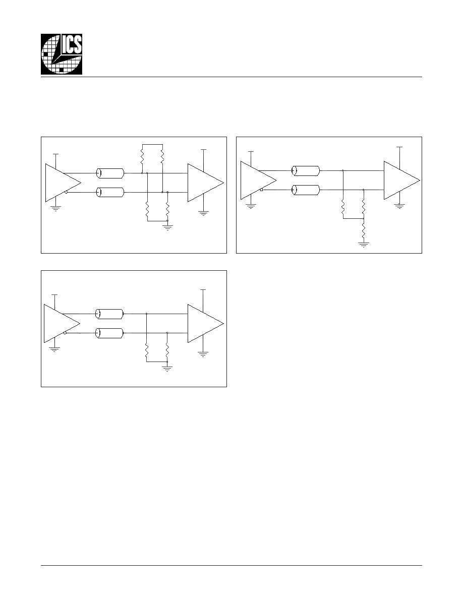
The CLK /nCLK accepts LVDS, LVPECL, LVHSTL, SSTL, HCSL
and other differential signals. Both V
SWING
and V
OH
must meet the
V
PP
and V
CMR
input requirements. Figures 4A to4E show inter-
face examples for the HiPerClockS CLK/nCLK input driven by
the most common driver types. The input interfaces suggested
F
IGURE
4A. H
I
P
ER
C
LOCK
S CLK/nCLK I
NPUT
D
RIVEN
BY
ICS H
I
P
ER
C
LOCK
S LVHSTL D
RIVER
here are examples only. Please consult with the vendor of the
driver component to confirm the driver termination requirements.
For example in
Figure 4A,
the input termination applies for ICS
HiPerClockS LVHSTL drivers. If you are using an LVHSTL driver
from another vendor, use their termination recommendation.
1.8V
R2
50
Input
LVHSTL Driver
ICS
HiPerClockS
R1
50
LVHSTL
3.3V
Zo = 50 Ohm
Zo = 50 Ohm
HiPerClockS
CLK
nCLK
F
IGURE
4E. H
I
P
ER
C
LOCK
S CLK/nCLK I
NPUT
D
RIVEN
BY
3.3V LVPECL D
RIVER
WITH
AC C
OUPLE
Zo = 50 Ohm
R3
125
HiPerClockS
CLK
nCLK
3.3V
R5
100 - 200
3.3V
R2
84
3.3V
R6
100 - 200
Input
R5,R6 locate near the driver pin.
Zo = 50 Ohm
R1
84
R4
125
C2
LVPECL
C1
Zo = 50 Ohm
R1
100
3.3V
LVDS_Driv er
Zo = 50 Ohm
Receiv er
CLK
nCLK
3.3V

813001AGI
www.icst.com/products/hiperclocks.html
REV. A SEPTEMBER 2, 2005
12
Integrated
Circuit
Systems, Inc.
ICS813001I
D
UAL
VCXO
W
/3.3V, 2.5V LVPECL
F
EMTO
C
LOCK
TM PLL
T
ERMINATION
FOR
3.3V LVPECL O
UTPUT
V
CC
- 2V
50
50
RTT
Z
o
= 50
Z
o
= 50
FOUT
FIN
RTT =
Z
o
1
((V
OH
+ V
OL
) / (V
CC
� 2)) � 2
3.3V
125
125
84
84
Z
o
= 50
Z
o
= 50
FOUT
FIN
The clock layout topology shown below is a typical ter-
mination for LVPECL outputs. The two different layouts
mentioned are recommended only as guidelines.
FOUT and nFOUT are low impedance follower outputs
that generate ECL/LVPECL compatible outputs. There-
fore, terminating resistors (DC current path to ground)
or current sources must be used for functionality. These
outputs are designed to drive 50
transmission lines.
F
IGURE
5B. LVPECL O
UTPUT
T
ERMINATION
F
IGURE
5A. LVPECL O
UTPUT
T
ERMINATION
Matched impedance techniques should be used to maxi-
mize operating frequency and minimize signal distor-
tion.
Figures 5A and 5B
show two different layouts which
are recommended only as guidelines. Other suitable
clock layouts may exist and it would be recommended
that the board designers simulate to guarantee compat-
ibility across all printed circuit and clock component pro-
cess variations.
I
NPUTS
:
C
RYSTAL
I
NPUT
:
For applications not requiring the use of the crystal oscillator
input, both XTAL_IN and XTAL_OUT can be left floating.
Though not required, but for additional protection, a 1k
resistor can be tied from XTAL_IN to ground.
CLK I
NPUT
:
For applications not requiring the use of a clock input, it can
be left floating. Though not required, but for additional
protection, a 1k
resistor can be tied from the CLK input to
ground.
CLK/nCLK I
NPUT
:
For applications not requiring the use of the differential input,
both CLK and nCLK can be left floating. Though not required,
but for additional protection, a 1k
resistor can be tied from
CLK to ground.
LVCMOS C
ONTROL
P
INS
:
All control pins have internal pull-ups or pull-downs; additional
resistance is not required but can be added for additional
protection. A 1k
resistor can be used.
VC input pin - do not float, must be biased.
R
ECOMMENDATIONS
FOR
U
NUSED
I
NPUT
AND
O
UTPUT
P
INS
O
UTPUTS
:
LVPECL O
UTPUT
All unused LVPECL outputs can be left floating. We
recommend that there is no trace attached. Both sides of the
differential output pair should either be left floating or
terminated.
813001AGI
www.icst.com/products/hiperclocks.html
REV. A SEPTEMBER 2, 2005
13
Integrated
Circuit
Systems, Inc.
ICS813001I
D
UAL
VCXO
W
/3.3V, 2.5V LVPECL
F
EMTO
C
LOCK
TM PLL
T
ERMINATION
FOR
2.5V LVPECL O
UTPUT
Figure 6A
and
Figure 6B
show examples of termination for
2.5V LVPECL driver. These terminations are equivalent to ter-
minating 50
to V
CC
- 2V. For V
CCO
= 2.5V, the V
CCO
- 2V is very
close to ground level. The R3 in Figure 6B can be eliminated
and the termination is shown in
Figure 6C.
F
IGURE
6C. 2.5V LVPECL T
ERMINATION
E
XAMPLE
R2
50
Zo = 50 Ohm
VCCO=2.5V
R1
50
Zo = 50 Ohm
+
-
2.5V
2,5V LVPECL
Driv er
F
IGURE
6B. 2.5V LVPECL D
RIVER
T
ERMINATION
E
XAMPLE
VCCO=2.5V
R1
50
R2
50
Zo = 50 Ohm
R3
18
2,5V LVPECL
Driv er
Zo = 50 Ohm
+
-
2.5V
F
IGURE
6A. 2.5V LVPECL D
RIVER
T
ERMINATION
E
XAMPLE
R2
62.5
2.5V
2,5V LVPECL
Driv er
R3
250
Zo = 50 Ohm
Zo = 50 Ohm
R4
62.5
2.5V
+
-
R1
250
VCCO=2.5V

813001AGI
www.icst.com/products/hiperclocks.html
REV. A SEPTEMBER 2, 2005
14
Integrated
Circuit
Systems, Inc.
ICS813001I
D
UAL
VCXO
W
/3.3V, 2.5V LVPECL
F
EMTO
C
LOCK
TM PLL
P
OWER
C
ONSIDERATIONS
This section provides information on power dissipation and junction temperature for the ICS813001I.
Equations and example calculations are also provided.
1. Power Dissipation.
The total power dissipation for the ICS813001I is the sum of the core power plus the power dissipated in the load(s).
The following is the power dissipation for V
CC
= 3.3V + 5% = 3.465V, which gives worst case results.
NOTE: Please refer to Section 3 for details on calculating power dissipated in the load.
�
Power (core)
MAX
= V
CC_MAX
* I
EE_MAX
= 3.465V * 130mA = 450.45mW
�
Power (outputs)
MAX
= 30mW/Loaded Output pair
Total Power
_MAX
(3.465V, with output switching) = 450.45mW + 30mW = 480.5mW
2. Junction Temperature.
Junction temperature, Tj, is the temperature at the junction of the bond wire and bond pad and directly affects the reliability of the
device. The maximum recommended junction temperature for HiPerClockS
TM
devices is 125�C.
The equation for Tj is as follows: Tj =
JA
* Pd_total + T
A
Tj = Junction Temperature
JA
= Junction-to-Ambient Thermal Resistance
Pd_total = Total Device Power Dissipation (example calculation is in section 1 above)
T
A
= Ambient Temperature
In order to calculate junction temperature, the appropriate junction-to-ambient thermal resistance
JA
must be used. Assuming a
moderate air flow of 1 meter per second and a multi-layer board, the appropriate value is 70�C/W per Table 8 below.
Therefore, Tj for an ambient temperature of 85�C with all outputs switching is:
85�C + 0.481W * 65�C/W = 116.3�C. This is below the limit of 125�C.
This calculation is only an example. Tj will obviously vary depending on the number of loaded outputs, supply voltage, air flow,
and the type of board (single layer or multi-layer).
T
ABLE
8. T
HERMAL
R
ESISTANCE
JA
FOR
24-
PIN
TSSOP, F
ORCED
C
ONVECTION
JA
by Velocity (Meters per Second)
0
1
2.5
Multi-Layer PCB, JEDEC Standard Test Boards
70�C/W
65�C/W
62�C/W

813001AGI
www.icst.com/products/hiperclocks.html
REV. A SEPTEMBER 2, 2005
15
Integrated
Circuit
Systems, Inc.
ICS813001I
D
UAL
VCXO
W
/3.3V, 2.5V LVPECL
F
EMTO
C
LOCK
TM PLL
3. Calculations and Equations.
The purpose of this section is to derive the power dissipated into the load.
LVPECL output driver circuit and termination are shown in
Figure 7.
T
o calculate worst case power dissipation into the load, use the following equations which assume a 50
load, and a termination
voltage of V
CCO
- 2V.
�
For logic high, V
OUT
= V
OH_MAX
= V
CCO_MAX
� 0.9V
(V
CCO_MAX
- V
OH_MAX
) = 0.9V
�
For logic low, V
OUT
= V
OL_MAX
= V
CCO_MAX
� 1.7V
(V
CCO_MAX
- V
OL_MAX
) = 1.7V
Pd_H is power dissipation when the output drives high.
Pd_L is the power dissipation when the output drives low.
Pd_H = [(V
OH_MAX
� (V
CCO_MAX
- 2V))/R
L
] * (V
CCO_MAX
- V
OH_MAX
) = [(2V - (V
CCO_MAX
- V
OH_MAX
))/R
L
] * (V
CCO_MAX
- V
OH_MAX
) =
[(2V - 0.9V)/50
] * 0.9V = 19.8mW
Pd_L = [(V
OL_MAX
� (V
CCO_MAX
- 2V))/R
L
] * (V
CCO_MAX
- V
OL_MAX
) = [(2V - (V
CCO_MAX
- V
OL_MAX
))/R
L
] * (V
CCO_MAX
- V
OL_MAX
) =
[(2V - 1.7V)/50
] * 1.7V = 10.2mW
Total Power Dissipation per output pair = Pd_H + Pd_L = 30mW
F
IGURE
7. LVPECL D
RIVER
C
IRCUIT
AND
T
ERMINATION
Q1
V
OUT
V
CCO
R L
50
V
CCO
- 2V

813001AGI
www.icst.com/products/hiperclocks.html
REV. A SEPTEMBER 2, 2005
16
Integrated
Circuit
Systems, Inc.
ICS813001I
D
UAL
VCXO
W
/3.3V, 2.5V LVPECL
F
EMTO
C
LOCK
TM PLL
R
ELIABILITY
I
NFORMATION
T
RANSISTOR
C
OUNT
The transistor count for ICS813001I is: 3948
T
ABLE
9.
JA
VS
. A
IR
F
LOW
T
ABLE
FOR
24 L
EAD
TSSOP
JA
by Velocity (Meters per Second)
0
1
2.5
Multi-Layer PCB, JEDEC Standard Test Boards
70�C/W
65�C/W
62�C/W

813001AGI
www.icst.com/products/hiperclocks.html
REV. A SEPTEMBER 2, 2005
17
Integrated
Circuit
Systems, Inc.
ICS813001I
D
UAL
VCXO
W
/3.3V, 2.5V LVPECL
F
EMTO
C
LOCK
TM PLL
P
ACKAGE
O
UTLINE
- G S
UFFIX
FOR
24 L
EAD
TSSOP
T
ABLE
10. P
ACKAGE
D
IMENSIONS
Reference Document: JEDEC Publication 95, MO-153
L
O
B
M
Y
S
s
r
e
t
e
m
i
l
l
i
M
m
u
m
i
n
i
M
m
u
m
i
x
a
M
N
4
2
A
-
-
0
2
.
1
1
A
5
0
.
0
5
1
.
0
2
A
0
8
.
0
5
0
.
1
b
9
1
.
0
0
3
.
0
c
9
0
.
0
0
2
.
0
D
0
7
.
7
0
9
.
7
E
C
I
S
A
B
0
4
.
6
1
E
0
3
.
4
0
5
.
4
e
C
I
S
A
B
5
6
.
0
L
5
4
.
0
5
7
.
0
�
0
�
8
a
a
a
-
-
0
1
.
0

813001AGI
www.icst.com/products/hiperclocks.html
REV. A SEPTEMBER 2, 2005
18
Integrated
Circuit
Systems, Inc.
ICS813001I
D
UAL
VCXO
W
/3.3V, 2.5V LVPECL
F
EMTO
C
LOCK
TM PLL
T
ABLE
11. O
RDERING
I
NFORMATION
While the information presented herein has been checked for both accuracy and reliability, Integrated Circuit Systems, Incorporated (ICS) assumes no responsibility for either its use or
for infringement of any patents or other rights of third parties, which would result from its use. No other circuits, patents, or licenses are implied. This product is intended for use in normal
commercial and industrial applications. Any other applications such as those requiring high reliability or other extraordinary environmental requirements are not recommended
without additional processing by ICS. ICS reserves the right to change any circuitry or specifications without notice. ICS does not authorize or warrant any ICS product for use in
life support devices or critical medical instruments.
The aforementioned trademarks, HiPerClockS and FemtoClocks are trademarks of Integrated Circuit Systems, Inc. or its subsidiaries in the United States and/or other countries.
r
e
b
m
u
N
r
e
d
r
O
/
t
r
a
P
g
n
i
k
r
a
M
e
g
a
k
c
a
P
g
n
i
g
a
k
c
a
P
g
n
i
p
p
i
h
S
e
r
u
t
a
r
e
p
m
e
T
I
G
A
1
0
0
3
1
8
S
C
I
I
G
A
1
0
0
3
1
8
S
C
I
P
O
S
S
T
d
a
e
L
4
2
e
b
u
t
C
�
5
8
o
t
C
�
0
4
-
T
I
G
A
1
0
0
3
1
8
S
C
I
I
G
A
1
0
0
3
1
8
S
C
I
P
O
S
S
T
d
a
e
L
4
2
l
e
e
r
&
e
p
a
t
0
0
5
2
C
�
5
8
o
t
C
�
0
4
-
F
L
I
G
A
1
0
0
3
1
8
S
C
I
L
I
G
A
1
0
0
3
1
8
S
C
I
P
O
S
S
T
"
e
e
r
F
-
d
a
e
L
"
d
a
e
L
4
2
e
b
u
t
C
�
5
8
o
t
C
�
0
4
-
T
F
L
I
G
A
1
0
0
3
1
8
S
C
I
L
I
G
A
1
0
0
3
1
8
S
C
I
P
O
S
S
T
"
e
e
r
F
-
d
a
e
L
"
d
a
e
L
4
2
l
e
e
r
&
e
p
a
t
0
0
5
2
C
�
5
8
o
t
C
�
0
4
-
.
t
n
a
il
p
m
o
c
S
H
o
R
e
r
a
d
n
a
n
o
i
t
a
r
u
g
i
f
n
o
c
e
e
r
F
-
b
P
e
h
t
e
r
a
r
e
b
m
u
n
t
r
a
p
e
h
t
o
t
x
i
f
f
u
s
F
L
n
a
h
t
i
w
d
e
r
e
d
r
o
e
r
a
t
a
h
t
s
t
r
a
P
:
E
T
O
N