 | –≠–ª–µ–∫—Ç—Ä–æ–Ω–Ω—ã–π –∫–æ–º–ø–æ–Ω–µ–Ω—Ç: ICS83023I | –°–∫–∞—á–∞—Ç—å:  PDF PDF  ZIP ZIP |

Integrated
Circuit
Systems, Inc.
ICS932S203
0601E--12/22/04
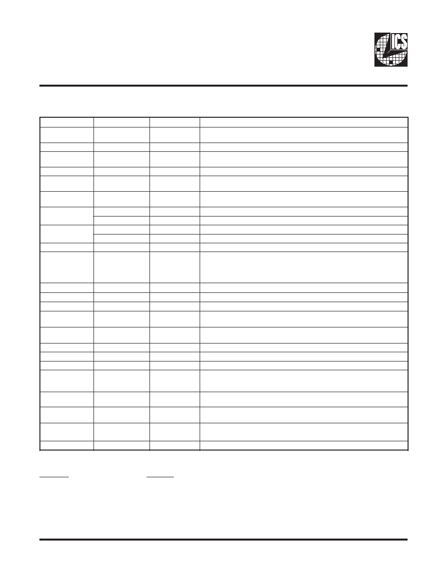
Block Diagram
Recommended Application:
Servers based on Intel CK408 processors
Output Features:
∑
4 Differential CPU Clock Pairs @ 3.3V
∑
7 PCI (3.3V) @ 33.3MHz
∑
3 PCI_F (3.3V) @ 33.3MHz
∑
1 USB (3.3V) @ 48MHz
∑
1 DOT (3.3V) @ 48MHz
∑
1 REF (3.3V) @ 14.318MHz
∑
1 3V66 (3.3V) @ 66.6MHz
∑
1 VCH/3V66 (3.3V) @ 48MHz or 66.6MHz
∑
3 66MHz_OUT/3V66 (3.3V) @ 66.6MHz_IN
or 66.6MHz
∑
1 66MHz_IN/3V66 (3.3V) @ Input/66MHz
Features:
∑
Supports spread spectrum modulation,
down spread 0 to -0.5%.
∑
Efficient power management scheme through PD#
and PCI_STOP#.
∑
Uses external 14.318MHz crystal
∑
Stop clocks and functional control available through
SMBus interface.
Key Specifications:
∑
CPU Output Jitter <150ps
∑
3V66 Output Jitter <250ps
∑
CPU Output Skew <150ps
Pin Configuration
56-Pin 300mil SSOP/TSSOP
Frequency Generator with 133MHz Differential CPU Clocks
Functionality
* These inputs have 150K internal pull-up resistor to VDD.
1
S
F
0
S
F
U
P
C
)
z
H
M
(
6
6
V
3
)
z
H
M
(
]
0
:
2
[
f
f
u
B
6
6
]
2
:
4
[
6
6
V
3
)
z
H
M
(
F
_
I
C
P
I
C
P
)
z
H
M
(
1
0
0
0
1
6
.
6
6
h
t
a
p
n
I
6
.
6
6
2
/
n
i
6
.
6
6
1
1
3
.
3
3
1
6
.
6
6
h
t
a
p
n
I
.
6
6
2
/
n
i
6
.
6
6
0
0
0
0
1
6
.
6
6
6
.
6
6
3
.
3
3
0
1
3
.
3
3
1
6
.
6
6
6
.
6
6
3
.
3
3
d
i
m
0
Z
-
i
H
Z
-
i
H
Z
-
i
H
Z
-
i
H
d
i
m
1
2
/
k
l
c
T
4
/
k
l
c
T
4
/
k
l
c
T
8
/
k
l
c
T
2
ICS932S203
0601E--12/22/04
Pin Configuration
R
E
B
M
U
N
N
I
P
E
M
A
N
N
I
P
E
P
Y
T
N
O
I
T
P
I
R
C
S
E
D
,
6
2
,
9
1
,
4
1
,
8
,
1
0
5
,
6
4
,
7
3
,
2
3
D
D
V
R
W
P
y
l
p
p
u
s
r
e
w
o
p
V
3
.
3
2
1
X
t
u
p
n
I
l
a
t
s
y
r
C
2
X
t
u
p
n
i
l
a
t
s
y
r
C
z
H
M
8
1
3
.
4
1
3
2
X
l
a
t
s
y
r
C
1
X
t
u
p
t
u
O
t
u
p
t
u
o
l
a
t
s
y
r
C
z
H
M
8
1
3
.
4
1
5
,
6
,
7
)
0
:
2
(
F
_
K
L
C
I
C
P
T
U
O
.
t
n
e
m
e
g
a
n
a
m
r
e
w
o
p
r
o
f
#
P
O
T
S
_
I
C
P
y
b
d
e
t
c
e
f
f
a
t
o
n
k
c
o
l
c
I
C
P
g
n
i
n
n
u
r
e
e
r
F
,
7
2
,
0
2
,
5
1
,
9
,
4
7
4
,
1
4
,
6
3
,
1
3
D
N
G
R
W
P
y
l
p
p
u
s
V
3
.
3
r
o
f
s
n
i
p
d
n
u
o
r
G
,
3
1
,
6
1
,
7
1
,
8
1
0
1
,
1
1
,
2
1
)
0
:
6
(
K
L
C
I
C
P
T
U
O
s
t
u
p
t
u
o
k
c
o
l
c
I
C
P
1
2
,
2
2
,
3
2
)
0
:
2
(
T
U
O
_
z
H
M
6
6
T
U
O
.
t
u
p
n
i
N
I
_
z
H
M
6
6
m
o
r
f
T
U
O
_
z
H
M
6
6
d
e
r
e
f
f
u
b
z
H
M
6
6
)
2
:
4
(
6
6
V
3
T
U
O
O
C
V
l
a
n
r
e
t
n
i
m
o
r
f
,
s
k
c
o
l
c
e
c
n
e
r
e
f
e
r
z
H
M
6
6
4
2
N
I
_
z
H
M
6
6
N
I
s
k
c
o
l
c
I
C
P
d
n
a
T
U
O
_
z
H
M
6
6
d
e
r
e
f
f
u
b
o
t
t
u
p
n
i
z
H
M
6
6
5
_
6
6
V
3
T
U
O
O
C
V
l
a
n
r
e
t
n
i
m
o
r
f
,
k
c
o
l
c
e
c
n
e
r
e
f
e
r
z
H
M
6
6
5
2
#
D
P
N
I
.
w
o
L
e
v
i
t
c
A
.
e
d
o
m
n
w
o
d
-
r
e
w
o
p
s
e
k
o
v
n
I
8
2
#
D
G
R
W
P
_
t
t
V
N
I
e
n
i
m
r
e
t
e
d
o
t
d
e
s
u
e
b
o
r
t
s
e
v
i
t
i
s
n
e
s
l
e
v
e
l
a
s
i
t
u
p
n
i
L
T
T
V
L
V
3
.
3
s
i
h
T
e
b
o
t
y
d
a
e
r
e
r
a
d
n
a
d
il
a
v
e
r
a
s
t
u
p
n
i
0
L
E
S
I
T
L
U
M
d
n
a
]
2
:
0
[
S
F
n
e
h
w
d
e
l
p
m
a
s
)
w
o
l
e
v
i
t
c
a
(
9
2
A
T
A
D
S
O
/
I
t
n
a
r
e
l
o
t
V
5
y
r
t
i
u
c
r
i
c
s
u
B
M
S
r
o
f
n
i
p
a
t
a
D
0
3
K
L
C
S
N
I
t
n
a
r
e
l
o
t
V
5
y
r
t
i
u
c
r
i
c
s
u
B
M
S
f
o
n
i
p
k
c
o
l
C
3
3
0
_
6
6
V
3
T
U
O
O
C
V
l
a
n
r
e
t
n
i
m
o
r
f
,
s
k
c
o
l
c
e
c
n
e
r
e
f
e
r
z
H
M
6
6
4
3
#
P
O
T
S
_
I
C
P
N
I
t
p
e
c
x
e
w
o
l
t
u
p
n
i
n
e
h
w
,
l
e
v
e
l
0
c
i
g
o
l
t
a
s
k
c
o
l
c
K
L
C
I
C
P
s
t
l
a
H
g
n
i
n
n
u
r
e
e
r
f
e
r
a
h
c
i
h
w
F
_
K
L
C
I
C
P
5
3
K
L
C
_
H
C
V
/
1
_
6
6
V
3
T
U
O
h
g
u
o
r
h
t
e
l
b
a
t
c
e
l
e
s
t
u
p
t
u
o
V
3
.
3
I
2
C
r
o
O
C
V
l
a
n
r
e
t
n
i
m
o
r
f
z
H
M
6
6
e
b
o
t
)
C
S
S
-
n
o
n
(
z
H
M
8
4
8
3
T
O
D
_
z
H
M
8
4
T
U
O
T
O
D
r
o
f
k
c
o
l
c
t
u
p
t
u
o
z
H
M
8
4
9
3
B
S
U
_
z
H
M
8
4
T
U
O
B
S
U
r
o
f
k
c
o
l
c
t
u
p
t
u
o
z
H
M
8
4
5
5
,
0
4
)
0
:
1
(
S
F
N
I
n
o
i
t
c
e
l
e
s
e
d
o
M
r
o
f
t
u
p
n
i
V
3
.
3
l
a
i
c
e
p
S
2
4
F
E
R
I
T
U
O
n
i
p
s
i
h
T
.
s
r
i
a
p
K
L
C
U
P
C
e
h
t
r
o
f
t
n
e
r
r
u
c
e
c
n
e
r
e
f
e
r
e
h
t
s
e
h
s
il
b
a
t
s
e
n
i
p
s
i
h
T
e
h
t
h
s
il
b
a
t
s
e
o
t
r
e
d
r
o
n
i
d
n
u
o
r
g
o
t
d
e
i
t
r
o
t
s
i
s
e
r
n
o
i
s
i
c
e
r
p
d
e
x
i
f
a
s
e
r
i
u
q
e
r
.
t
n
e
r
r
u
c
e
t
a
i
r
p
o
r
p
p
a
3
4
0
L
E
S
T
L
U
M
N
I
o
t
r
o
i
r
p
d
e
h
c
t
a
l
y
ll
a
n
r
e
t
n
i
n
e
h
t
d
n
a
p
u
-
r
e
w
o
p
n
o
d
e
s
n
e
s
s
i
t
u
p
n
i
0
L
E
S
T
L
U
M
.
s
k
c
o
l
c
z
H
M
8
1
3
.
4
1
V
3
n
o
t
u
p
t
u
o
r
o
f
d
e
s
u
g
n
i
e
b
n
i
p
e
h
t
3
5
,
1
5
,
8
4
,
4
4
)
0
:
3
(
C
K
L
C
U
P
C
T
U
O
t
n
e
r
r
u
c
e
r
a
e
s
e
h
T
.
s
t
u
p
t
u
o
U
P
C
r
i
a
p
l
a
i
t
n
e
r
e
f
f
i
d
f
o
s
k
c
o
l
c
"
y
r
a
t
n
e
m
e
l
p
m
o
C
"
.
s
a
i
b
e
g
a
t
l
o
v
r
o
f
d
e
r
i
u
q
e
r
e
r
a
s
r
o
t
s
i
s
e
r
l
a
n
r
e
t
x
e
d
n
a
s
t
u
p
t
u
o
4
5
,
2
5
,
9
4
,
5
4
)
0
:
3
(
T
K
L
C
U
P
C
T
U
O
d
n
a
s
t
u
p
t
u
o
t
n
e
r
r
u
c
e
r
a
e
s
e
h
T
.
s
t
u
p
t
u
o
U
P
C
r
i
a
p
l
a
i
t
n
e
r
e
f
f
i
d
f
o
s
k
c
o
l
c
"
e
u
r
T
"
.
s
a
i
b
e
g
a
t
l
o
v
r
o
f
d
e
r
i
u
q
e
r
e
r
a
s
r
o
t
s
i
s
e
r
l
a
n
r
e
t
x
e
6
5
F
E
R
T
U
O
.
k
c
o
l
c
e
c
n
e
r
e
f
e
r
z
H
M
8
1
3
.
4
1
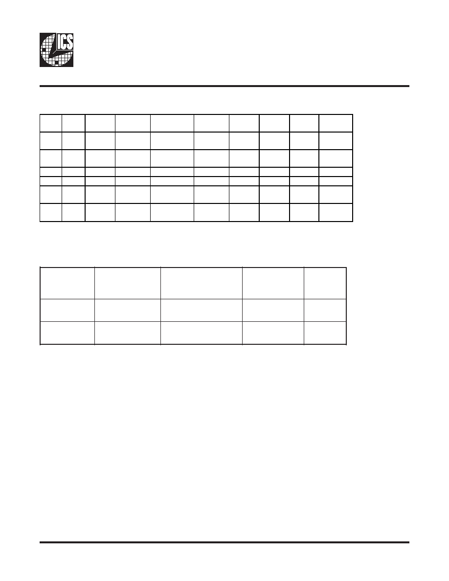
Power Groups
(Analog)
VDDA = PLL1
VDD48 = 48MHz, PLL
VDDREF = VDD for Xtal, POR
(Digital)
VDDPCI
VDD3V66
VDDCPU
3
ICS932S203
0601E--12/22/04
Frequency Select Table
Host Swing Select Functions
0
L
E
S
I
T
L
U
M
t
e
g
r
a
T
d
r
a
o
B
Z
m
r
e
T
/
e
c
a
r
T
,
R
e
c
n
e
r
e
f
e
R
=
f
e
r
I
V
D
D
)
r
R
*
3
(
/
t
u
p
t
u
O
t
n
e
r
r
u
C
Z
@
h
o
V
0
s
m
h
o
0
5
,
%
1
1
2
2
=
r
R
A
m
0
0
.
5
=
f
e
r
I
F
E
R
I
*
4
=
h
o
I
0
5
@
V
0
.
1
1
s
m
h
o
0
5
,
%
1
5
7
4
=
r
R
A
m
2
3
.
2
=
f
e
r
I
F
E
R
I
*
6
=
h
o
I
0
5
@
V
7
.
0
FS2
FS1
CPU
3V66 (1:0)
66Buff (2:0) /
3V66 (4:2)
66 In /
3V66_5
PCI
REF
USB,
DOT
note
1
0
100
66.6
66.6 In path
66.6 IN
66.6 in/2
14.318
48
Buffer
mode 66
1
1
133.3
66.6
66.6 In path
66.6 IN
66.6 in/2
14.318
48
Buffer
mode 66
0
0
100
66.6
66.6
66.6
33.3
14.318
48
Driven 66
0
1
133.3
66.6
66.6
66.6
33.3
14.318
48
Driven 66
mid
0
Hi-Z
Hi-Z
Hi-Z
Hi-Z
Hi-Z
Hi-Z
Hi-Z
Tri-state
outputs
mid
1
Tclk/2
Tclk/4
Tclk/4
Tclk/4
Tclk/8
Tclk
Tclk/2
Tclk is at
X1 input

4
ICS932S203
0601E--12/22/04
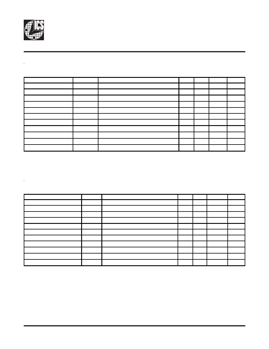
Byte 0: Control Register
Notes:
1. R= Read only RW= Read and Write
2. PWD = Power on Default
3. The purpose of this bit is to allow a system designer to implement PCI_STOP functionality in one of two ways.
Wither the system designer can choose to use the externally provided PCI_STOP# pin to assert and de-assert
PCI_STOP functionality via SMBus Byte 0 Bit 3.
In Hardware mode it is not allowed to write to the SMBus Byte 0 Bit3. In Software mode it is not allowed to pull
the external PCI_STOP pin low. This avoids the issues related with Hardware started and software stopped
PCI_STOP conditions. The clock chip is to be operated in the Hardware or Software PCI_STOP mode ONLY, it
is not allowed to mix these modes.
In Hardware mode the SMBus byte 0 Bit 3 is R/W and should reflect the status of the part. Whether or not the
chip is in PCI_STOP mode.
Functionality PCI_STOP mode should be entered when [(PCI_STOP#=0) or (SMBus Byte 0 Bit 3 = 0)].
Byte 1: Control Register
t
i
B
#
n
i
P
e
m
a
N
D
W
P
e
p
y
T
n
o
i
t
p
i
r
c
s
e
D
0
t
i
B
-
1
)
d
e
v
r
e
s
e
R
(
1
t
i
B
5
5
0
S
F
X
R
p
u
r
e
w
o
p
n
o
d
e
l
p
m
a
s
n
i
p
0
S
F
f
o
e
u
l
a
v
e
h
t
s
t
c
e
l
f
e
R
2
t
i
B
0
4
1
S
F
X
R
p
u
r
e
w
o
p
n
o
d
e
l
p
m
a
s
n
i
p
1
S
F
f
o
e
u
l
a
v
e
h
t
s
t
c
e
l
f
e
R
3
t
i
B
4
3
#
P
O
T
S
_
I
C
P
3
X
R
#
P
O
T
S
_
I
C
P
f
o
e
u
l
a
v
e
h
t
s
t
c
e
l
f
e
R
:
e
d
o
m
e
r
a
w
d
r
a
H
D
W
P
n
o
d
e
l
p
m
a
s
n
i
p
4
t
i
B
-
1
)
d
e
v
r
e
s
e
R
(
5
t
i
B
5
3
H
C
V
/
1
_
6
6
V
3
0
W
R
z
H
M
8
4
/
z
H
M
6
6
t
c
e
l
e
S
H
C
V
z
H
M
8
4
=
1
,
z
H
M
6
6
=
0
6
t
i
B
-
0
)
d
e
v
r
e
s
e
R
(
7
t
i
B
-
d
a
e
r
p
S
d
e
l
b
a
n
E
0
W
R
n
O
d
a
e
r
p
S
=
1
,
f
f
O
d
a
e
r
p
S
=
0
t
i
B
#
n
i
P
e
m
a
N
D
W
P
e
p
y
T
n
o
i
t
p
i
r
c
s
e
D
0
t
i
B
1
5
,
2
5
0
T
K
L
C
U
P
C
0
C
K
L
C
U
P
C
1
W
R
d
e
l
b
a
n
E
=
1
d
e
l
b
a
s
i
D
=
0
1
t
i
B
8
4
,
9
4
1
T
K
L
C
U
P
C
1
C
K
L
C
U
P
C
1
W
R
d
e
l
b
a
n
E
=
1
d
e
l
b
a
s
i
D
=
0
2
t
i
B
4
4
,
5
4
2
T
K
L
C
U
P
C
2
C
K
L
C
U
P
C
1
W
R
d
e
l
b
a
n
E
=
1
d
e
l
b
a
s
i
D
=
0
3
t
i
B
1
5
,
2
5
0
-
d
e
v
r
e
s
e
R
4
t
i
B
8
4
,
9
4
0
-
d
e
v
r
e
s
e
R
5
t
i
B
4
4
,
5
4
0
-
d
e
v
r
e
s
e
R
6
t
i
B
4
5
,
3
5
3
T
K
L
C
U
P
C
3
C
K
L
C
U
P
C
1
W
R
d
e
l
b
a
n
E
=
1
d
e
l
b
a
s
i
D
=
0
7
t
i
B
3
4
0
L
E
S
T
L
U
M
X
R
0
L
E
S
T
L
U
M
f
o
e
u
l
a
v
t
n
e
r
r
u
c
e
h
t
s
t
c
e
l
f
e
R

5
ICS932S203
0601E--12/22/04
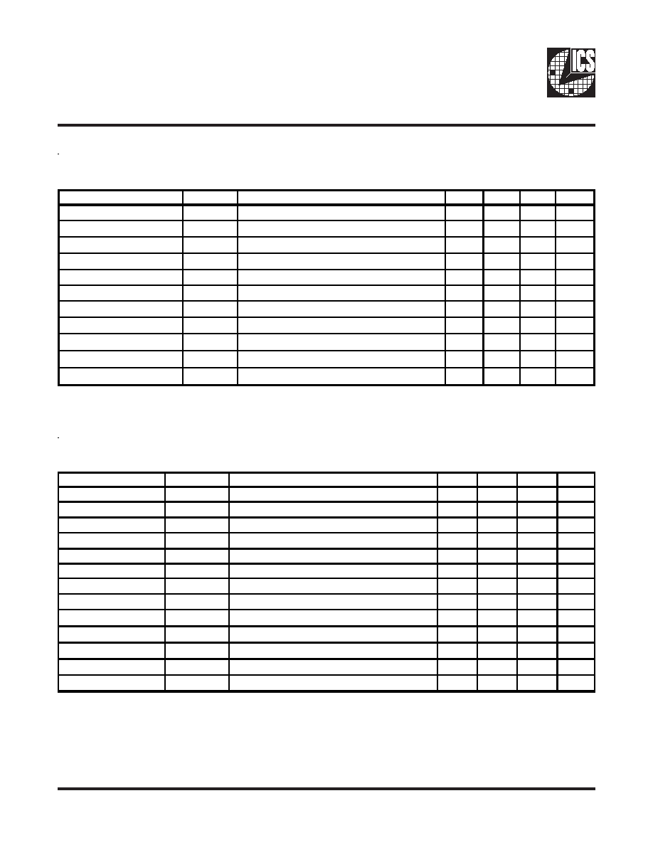
Byte 2: Control Register
Notes:
1. R= Read only RW= Read and Write
2. PWD = Power on Default
t
i
B
#
n
i
P
e
m
a
N
D
W
P
e
p
y
T
n
o
i
t
p
i
r
c
s
e
D
0
t
i
B
0
1
0
K
L
C
I
C
P
1
W
R
d
e
l
b
a
n
E
=
1
d
e
l
b
a
s
i
D
=
0
1
t
i
B
1
1
1
K
L
C
I
C
P
1
W
R
d
e
l
b
a
n
E
=
1
d
e
l
b
a
s
i
D
=
0
2
t
i
B
2
1
2
K
L
C
I
C
P
1
W
R
d
e
l
b
a
n
E
=
1
d
e
l
b
a
s
i
D
=
0
3
t
i
B
3
1
3
K
L
C
I
C
P
1
W
R
d
e
l
b
a
n
E
=
1
d
e
l
b
a
s
i
D
=
0
4
t
i
B
6
1
4
K
L
C
I
C
P
1
W
R
d
e
l
b
a
n
E
=
1
d
e
l
b
a
s
i
D
=
0
5
t
i
B
7
1
5
K
L
C
I
C
P
1
W
R
d
e
l
b
a
n
E
=
1
d
e
l
b
a
s
i
D
=
0
6
t
i
B
8
1
6
K
L
C
I
C
P
1
W
R
d
e
l
b
a
n
E
=
1
d
e
l
b
a
s
i
D
=
0
7
t
i
B
-
-
0
-
)
d
e
v
r
e
s
e
R
(
Byte 3: Control Register
Byte 4: Control Register
t
i
B
#
n
i
P
e
m
a
N
D
W
P
e
p
y
T
n
o
i
t
p
i
r
c
s
e
D
0
t
i
B
1
2
2
-
6
6
V
3
/
0
T
U
O
_
z
H
M
6
6
1
W
R
d
e
l
b
a
n
E
=
1
d
e
l
b
a
s
i
D
=
0
1
t
i
B
2
2
3
-
6
6
V
3
/
0
T
U
O
_
z
H
M
6
6
1
W
R
d
e
l
b
a
n
E
=
1
d
e
l
b
a
s
i
D
=
0
2
t
i
B
3
2
4
-
6
6
V
3
/
0
T
U
O
_
z
H
M
6
6
1
W
R
d
e
l
b
a
n
E
=
1
d
e
l
b
a
s
i
D
=
0
3
t
i
B
4
2
5
_
6
6
V
3
1
W
R
d
e
l
b
a
n
E
=
1
d
e
l
b
a
s
i
D
=
0
4
t
i
B
5
3
K
L
C
_
H
C
V
/
1
_
6
6
V
3
1
W
R
d
e
l
b
a
n
E
=
1
d
e
l
b
a
s
i
D
=
0
5
t
i
B
3
3
0
_
6
6
V
3
1
W
R
d
e
l
b
a
n
E
=
1
d
e
l
b
a
s
i
D
=
0
6
t
i
B
-
-
0
R
)
d
e
v
r
e
s
e
R
(
7
t
i
B
-
-
0
R
)
d
e
v
r
e
s
e
R
(
t
i
B
#
n
i
P
e
m
a
N
D
W
P
e
p
y
T
n
o
i
t
p
i
r
c
s
e
D
0
t
i
B
5
0
F
_
K
L
C
I
C
P
1
W
R
d
e
l
b
a
n
E
=
1
d
e
l
b
a
s
i
D
=
0
1
t
i
B
6
1
F
_
K
L
C
I
C
P
1
W
R
d
e
l
b
a
n
E
=
1
d
e
l
b
a
s
i
D
=
0
2
t
i
B
7
2
F
_
K
L
C
I
C
P
1
W
R
d
e
l
b
a
n
E
=
1
d
e
l
b
a
s
i
D
=
0
3
t
i
B
5
0
F
_
K
L
C
I
C
P
0
W
R
f
o
n
o
i
t
r
e
s
s
a
h
t
i
w
0
F
_
K
L
C
I
C
P
f
o
l
o
r
t
n
o
c
w
o
ll
A
g
n
i
n
n
u
r
e
e
r
f
t
o
N
=
1
,
g
n
i
n
n
u
R
e
e
r
F
=
0
.
#
P
O
T
S
_
I
C
P
4
t
i
B
6
1
F
_
K
L
C
I
C
P
0
W
R
f
o
n
o
i
t
r
e
s
s
a
h
t
i
w
1
F
_
K
L
C
I
C
P
f
o
l
o
r
t
n
o
c
w
o
ll
A
g
n
i
n
n
u
r
e
e
r
f
t
o
N
=
1
,
g
n
i
n
n
u
R
e
e
r
F
=
0
.
#
P
O
T
S
_
I
C
P
5
t
i
B
7
2
F
_
K
L
C
I
C
P
0
W
R
f
o
n
o
i
t
r
e
s
s
a
h
t
i
w
2
F
_
K
L
C
I
C
P
f
o
l
o
r
t
n
o
c
w
o
ll
A
g
n
i
n
n
u
r
e
e
r
f
t
o
N
=
1
,
g
n
i
n
n
u
R
e
e
r
F
=
0
.
#
P
O
T
S
_
I
C
P
6
t
i
B
9
3
B
S
U
_
z
H
M
8
4
1
W
R
d
e
l
b
a
n
E
=
1
d
e
l
b
a
s
i
D
=
0
7
t
i
B
8
3
T
O
D
_
z
H
M
8
4
1
W
R
d
e
l
b
a
n
E
=
1
d
e
l
b
a
s
i
D
=
0
6
ICS932S203
0601E--12/22/04
Byte 6: Vendor ID Register
(1 = enable, 0 = disable)
t
i
B
#
n
i
P
e
m
a
N
D
W
P
e
p
y
T
n
o
i
t
p
i
r
c
s
e
D
0
t
i
B
X
0
t
i
B
D
I
r
o
d
n
e
V
1
R
)
d
e
v
r
e
s
e
R
(
1
t
i
B
X
1
t
i
B
D
I
r
o
d
n
e
V
0
R
)
d
e
v
r
e
s
e
R
(
2
t
i
B
X
2
t
i
B
D
I
r
o
d
n
e
V
0
R
)
d
e
v
r
e
s
e
R
(
3
t
i
B
X
3
t
i
B
D
I
r
o
d
n
e
V
0
R
)
d
e
v
r
e
s
e
R
(
4
t
i
B
X
0
t
i
B
D
I
n
o
i
s
i
v
e
R
X
R
n
o
d
e
s
a
b
e
b
ll
i
w
s
e
u
l
a
v
D
I
n
o
i
s
i
v
e
R
n
o
i
s
i
v
e
r
s
'
e
c
i
v
e
d
l
a
u
d
i
v
i
d
n
i
5
t
i
B
X
1
t
i
B
D
I
n
o
i
s
i
v
e
R
X
R
6
t
i
B
X
2
t
i
B
D
I
n
o
i
s
i
v
e
R
X
R
7
t
i
B
X
3
t
i
B
D
I
n
o
i
s
i
v
e
R
X
R
Byte 5: Programming Edge Rate
(1 = enable, 0 = disable)
Notes:
1. R= Read only RW= Read and Write
2. PWD = Power on Default
t
i
B
#
n
i
P
e
m
a
N
D
W
P
e
p
y
T
n
o
i
t
p
i
r
c
s
e
D
0
t
i
B
X
B
S
U
_
z
H
M
8
4
0
W
R
l
o
r
t
n
c
e
t
a
r
e
g
d
e
B
S
U
1
t
i
B
X
B
S
U
_
z
H
M
8
4
0
W
R
l
o
r
t
n
c
e
t
a
r
e
g
d
e
B
S
U
2
t
i
B
X
T
O
D
_
z
H
M
8
4
0
W
R
l
o
r
t
n
o
c
e
t
a
r
e
g
d
e
T
O
D
3
t
i
B
X
T
O
D
_
z
H
M
8
4
0
W
R
l
o
r
t
n
o
c
e
t
a
r
e
g
d
e
T
O
D
4
t
i
B
X
-
0
-
)
d
e
v
r
e
s
e
R
(
5
t
i
B
X
-
0
-
)
d
e
v
r
e
s
e
R
(
6
t
i
B
X
-
0
-
)
d
e
v
r
e
s
e
R
(
7
t
i
B
X
-
0
-
)
d
e
v
r
e
s
e
R
(
7
ICS932S203
0601E--12/22/04
Absolute Maximum Ratings
Supply Voltage . . . . . . . . . . . . . . . . . . . . . . . . . 5.5 V
Logic Inputs . . . . . . . . . . . . . . . . . . . . . . . . . . . GND ≠0.5 V to V
DD
+0.5 V
Ambient Operating Temperature . . . . . . . . . . 0∞C to +70∞C
Case Temperature . . . . . . . . . . . . . . . . . . . . . . 115∞C
Storage Temperature . . . . . . . . . . . . . . . . . . . . ≠65∞C to +150∞C
Stresses above those listed under
Absolute Maximum Ratings may cause permanent damage to the device. These
ratings are stress specifications only and functional operation of the device at these or any other conditions above those
listed in the operational sections of the specifications is not implied. Exposure to absolute maximum rating conditions
for extended periods may affect product reliability.
Electrical Characteristics - Input/Supply/Common Output Parameters
T
A
= 0 - 70∞C; Supply Voltage V
DD
= 3.3 V +/-5%
PARAMETER
SYMBOL
CONDITIONS
MIN
TYP
MAX
UNITS
Input High Voltage
V
IH
2
V
DD
+ 0.3
V
Input Low Voltage
V
IL
V
SS
- 0.3
0.8
V
Input High Current
I
IH
V
IN
= V
DD
-5
5
mA
I
IL1
V
IN
= 0 V; Inputs with no pull-up resistors
-5
mA
I
IL2
V
IN
= 0 V; Inputs with pull-up resistors
-200
Operating Supply Current I
DD3.3OP
C
L
= Full load; Select @ 100 MHz
229
230
360
mA
I
DD3.3OP
C
L
=Full load; Select @ 133 MHz
220
233
360
mA
Powerdown Current
I
DD3.3PD
60
mA
Input Frequency
F
i
V
DD
= 3.3 V
14.318
MHz
Pin Inductance
L
pin
7
nH
C
IN
Logic Inputs
5
pF
C
OUT
Output pin capacitance
6
pF
C
INX
X1 & X2 pins
27
45
pF
Transition time
1
T
trans
To 1st crossing of target frequency
3
ms
Settling time
1
T
s
From 1st crossing to 1% target frequency
3
ms
Clk Stabilization
1
T
STAB
From V
DD
= 3.3 V to 1% target frequency
3
ms
t
PZH
,t
PZL
Output enable delay (all outputs)
1
10
ns
t
PHZ
,t
PLZ
Output disable delay (all outputs)
1
10
ns
1
Guaranteed by design, not 100% tested in production.
Delay
1
Input Capacitance
1
Input Low Current

8
ICS932S203
0601E--12/22/04
Electrical Characteristics - CPU 0.7V Current Mode Differential Pair
T
A
= 0 - 70∞C; V
DD
= 3.3 V +/-5%; C
L
=2pF
PARAMETER
SYMBOL
CONDITIONS
MIN
TYP
MAX
UNITS
NOTES
Current Source Output
Impedance
Zo
1
V
O
= V
x
3000
1
Voltage High
VHigh
660
770
850
1
Voltage Low
VLow
-150
5
150
1
Max Voltage
Vovs
756
1150
1
Min Voltage
Vuds
-300
-7
1
Crossing Voltage (abs) Vcross(abs)
250
350
550
mV
1
Crossing Voltage (var)
d-Vcross
Variation of crossing over all
edges
12
140
mV
1
Long Accuracy
ppm
see Tperiod min-max values
-300
300
ppm
1,2
200MHz nominal
4.9985
5.0015
ns
2
200MHz spread
4.9985
5.0266
ns
2
166.66MHz nominal
5.9982
6.0018
ns
2
166.66MHz spread
5.9982
6.0320
ns
2
133.33MHz nominal
7.4978
7.5023
ns
2
133.33MHz spread
7.4978
5.4000
ns
2
100.00MHz nominal
9.9970
10.0030
ns
2
100.00MHz spread
9.9970
10.0533
ns
2
200MHz nominal
4.8735
ns
1,2
166.66MHz nominal/spread
5.8732
ns
1,2
133.33MHz nominal/spread
7.3728
ns
1,2
100.00MHz nominal/spread
9.8720
ns
1,2
Rise Time
t
r
V
OL
= 0.175V, V
OH
= 0.525V
175
332
700
ps
1
Fall Time
t
f
V
OH
= 0.525V V
OL
= 0.175V
175
344
700
ps
1
Rise Time Variation
d-t
r
30
125
ps
1
Fall Time Variation
d-t
f
30
125
ps
1
Duty Cycle
d
t3
Measurement from differential
wavefrom
45
49
55
%
1
Skew
t
sk3
V
T
= 50%
8
100
ps
1
Jitter, Cycle to cycle
t
jcyc-cyc
Measurement from differential
wavefrom
60
150
ps
1
1
Guaranteed by design, not 100% tested in production.
2
All Long Term Accuracy and Clock Period specifications are guaranteed with the assumption that Ref output is at
14.31818MHz
Tperiod
Average period
Absolute min period
T
absmin
Statistical measurement on single
ended signal using oscilloscope
math function.
mV
Measurement on single ended
signal using absolute value.
mV
9
ICS932S203
0601E--12/22/04
Electrical Characteristics - PCICLK Un-Buffered Mode
T
A
= 0 - 70∞C; VDD=3.3V +/-5%; C
L
= 10-30 pF (unless otherwise specified)
PARAMETER
SYMBOL
CONDITIONS
MIN
TYP
MAX
UNITS
Output Frequency
F
O1
MHz
Output Impedance
R
DSP1
1
V
O
= V
DD
*(0.5)
12
33
55
Output High Voltage
V
OH
1
I
OH
= -1 mA
2.4
V
Output Low Voltage
V
OL
1
I
OL
= 1 mA
0.55
V
Output High Current
I
OH
1
V
OH@MIN
= 1.0 V, V
OH@MAX
= 3.135 V
-33
-33
mA
Output Low Current
I
OL
1
V
OL @MIN
= 1.95 V, V
OL @MAX
= 0.4 V
30
38
mA
Rise Time
t
r1
1
V
OL
= 0.4 V, V
OH
= 2.4 V
0.5
1.32
0.5to 2
ns
Fall Time
t
f1
1
V
OH
= 2.4 V, V
OL
= 0.4 V
0.5
1.39
0.5 to 2
ns
Duty Cycle
d
t1
1
V
T
= 1.5 V
45
52
55
%
Skew t
sk1
1
V
T
= 1.5 V
247
500
ps
Jitter,cycle to cyc
t
jcyc-cyc
1
V
T
= 1.5 V
111
500
ps
1
Guaranteed by design, not 100% tested in production.
Electrical Characteristics - PCICLK Buffered Mode
T
A
= 0 - 70∞C; VDD=3.3V +/-5%; C
L
= 10-30 pF (unless otherwise specified)
PARAMETER
SYMBOL
CONDITIONS
MIN
TYP
MAX
UNITS
Output Frequency
F
O1
MHz
Output Impedance
R
DSP1
1
V
O
= V
DD
*(0.5)
12
33
55
Output High Voltage
V
OH
1
I
OH
= -1 mA
2.4
V
Output Low Voltage
V
OL
1
I
OL
= 1 mA
0.55
V
Output High Current
I
OH
1
V
OH@MIN
= 1.0 V, V
OH@MAX
= 3.135 V
-33
-33
mA
Output Low Current
I
OL
1
V
OL @MIN
= 1.95 V, V
OL @MAX
= 0.4 V
30
38
mA
Rise Time
t
r1
1
V
OL
= 0.4 V, V
OH
= 2.4 V
0.5
1.29
0.5to 2
ns
Fall Time
t
f1
1
V
OH
= 2.4 V, V
OL
= 0.4 V
0.5
1.32
0.5 to 2
ns
Duty Cycle
d
t1
1
V
T
= 1.5 V
45
51.9
55
%
Skew t
sk1
1
V
T
= 1.5 V
209
500
ps
Jitter,cycle to cyc
t
jcyc-cyc
1
V
T
= 1.5 V
107
500
ps
1
Guaranteed by design, not 100% tested in production.
10
ICS932S203
0601E--12/22/04
Electrical Characteristics- 3V66 - Buffered Mode: 3V66 [1:0] 66MHz_OUT [2:0]
T
A
= 0 - 70C; VDD=3.3V +/-5%; C
L
= 10-30 pF (unless otherwise specified)
PARAMETER
SYMBOL
CONDITIONS
MIN
TYP
MAX
UNITS
Output Frequency
F
O1
66.66
MHz
Output Impedance
R
DSP1
1
V
O
= V
DD
*(0.5)
12
33
55
W
Output High Voltage
V
OH
1
I
OH
= -1 mA
2.4
V
Output Low Voltage
V
OL
1
I
OL
= 1 mA
0.55
V
Output High Current
I
OH
1
V
OH@MIN
= 1.0 V, V
OH@MAX
= 3.135 V
-33
-33
mA
Output Low Current
I
OL
1
V
OL @MIN
= 1.95 V, V
OL @MAX
= 0.4 V
30
38
mA
Rise Time
t
r1
1
V
OL
= 0.4 V, V
OH
= 2.4 V
0.5
1.44
2
ns
Fall Time
t
f1
1
V
OH
= 2.4 V, V
OL
= 0.4 V
0.5
1.36
2
ns
Duty Cycle
d
t1
1
V
T
= 1.5 V
45
54.6
55
%
Skew t
sk1
1
V
T
= 1.5 V 3V66 [1:0]
105
250
ps
Jitter
t
jcyc-cyc
1
V
T
= 1.5 V 3V66 [1:0]
121
300
ps
Skew t
sk1
1
V
T
= 1.5 V 66MHz_OUT [2:0]
169
250
ps
Jitter
t
jcyc-cyc
1
V
T
= 1.5 V 66MHz_OUT [2:0]
89
300
ps
1
Guaranteed by design, not 100% tested in production.
Electrical Characteristics - 3V66 -Un-Buffered Mode: 3V66 [5:0]
T
A
= 0 - 70∞C; VDD=3.3V +/-5%; C
L
= 10-30 pF (unless otherwise specified)
PARAMETER
SYMBOL
CONDITIONS
MIN
TYP
MAX UNITS
Output Frequency
F
O1
66.66
MHz
Output Impedance
R
DSP1
1
V
O
= V
DD
*(0.5)
12
33
55
Output High Voltage
V
OH
1
I
OH
= -1 mA
2.4
V
Output Low Voltage
V
OL
1
I
OL
= 1 mA
0.55
V
Output High Current
I
OH
1
V
OH@MIN
= 1.0 V, V
OH@MAX
= 3.135 V
-33
-33
mA
Output Low Current
I
OL
1
V
OL @MIN
= 1.95 V, V
OL @MAX
= 0.4 V
30
38
mA
Rise Time
t
r1
1
V
OL
= 0.4 V, V
OH
= 2.4 V
0.5
1.38
2
ns
Fall Time
t
f1
1
V
OH
= 2.4 V, V
OL
= 0.4 V
0.5
1.45
2
ns
Duty Cycle
d
t1
1
V
T
= 1.5 V
45
54.4
55
%
Skew t
sk1
1
V
T
= 1.5 V
90
250
ps
Jitter
t
jcyc-cyc
1
V
T
= 1.5 V 3V66
128
250
ps
1
Guaranteed by design, not 100% tested in production.

11
ICS932S203
0601E--12/22/04
Electrical Characteristics - REF
T
A
= 0 - 70∞C; VDD=3.3V +/-5%; C
L
= 10-20 pF (unless otherwise specified)
PARAMETER
SYMBOL
CONDITIONS
MIN
TYP
MAX
UNITS
Output Frequency
F
O1
MHz
Output Impedance
R
DSP1
1
V
O
= V
DD
*(0.5)
20
48
60
Output High Voltage
V
OH
1
I
OH
= -1 mA
2.4
V
Output Low Voltage
V
OL
1
I
OL
= 1 mA
0.4
V
Output High Current
I
OH
1
V
OH@MIN
= 1.0 V, V
OH@MAX
= 3.135 V
-29
-23
mA
Output Low Current
I
OL
1
V
OL @MIN
= 1.95 V, V
OL @MAX
= 0.4 V
29
27
mA
Rise Time
t
r1
1
V
OL
= 0.4 V, V
OH
= 2.4 V
1
1.25
2
ns
Fall Time
t
f1
1
V
OH
= 2.4 V, V
OL
= 0.4 V
1
1.15
2
ns
Duty Cycle
d
t1
1
V
T
= 1.5 V
45
53
55
%
Jitter
t
jcyc-cyc
1
V
T
= 1.5 V
723
1000
ps
1
Guaranteed by design, not 100% tested in production.
Electrical Characteristics - VCH, 48MHz DOT, 48MHz, USB
T
A
= 0 - 70∞C; VDD=3.3V +/-5%; C
L
= 10-20 pF (unless otherwise specified)
PARAMETER
SYMBOL
CONDITIONS
MIN
TYP
MAX
UNITS
Output Frequency
F
O1
48
MHz
Output Impedance
R
DSP1
1
V
O
= V
DD
*(0.5)
20
48
60
Output High Voltage
V
OH
1
I
OH
= -1 mA
2.4
V
Output Low Voltage
V
OL
1
I
OL
= 1 mA
0.4
V
Output High Current
I
OH
1
V
OH@MIN
= 1.0 V, V
OH@MAX
= 3.135 V
-29
-23
mA
Output Low Current
I
OL
1
V
OL @MIN
= 1.95 V, V
OL @MAX
= 0.4 V
29
27
mA
48DOT Rise Time
t
r1
1
V
OL
= 0.4 V, V
OH
= 2.4 V
0.5
0.6
1
ns
48DOT Fall Time
t
f1
1
V
OH
= 2.4 V, V
OL
= 0.4 V
0.5
0.8
1
ns
VCH 48 USB Rise Time
t
r1
1
V
OL
= 0.4 V, V
OH
= 2.4 V
1
1.2
2
ns
VCH 48 USB Fall Time
t
f1
1
V
OH
= 2.4 V, V
OL
= 0.4 V
1
1.3
2
ns
48 DOT Duty Cycle
d
t1
1
V
T
= 1.5 V
45
52.8
55
%
VCH 48 USB Duty Cycle
d
t1
1
V
T
= 1.5 V
45
53.5
55
%
48 DOT Jitter
t
jcyc-cyc
1
V
T
= 1.5 V
183
350
ps
VCH Jitter
t
jcyc-cyc
1
V
T
= 1.5 V
223
350
ps
1
Guaranteed by design, not 100% tested in production.

12
ICS932S203
0601E--12/22/04
1.
The ICS clock generator is a slave/receiver, SMBus component. It can read back the data stored in the latches
for verification. Read-Back will support Intel PIIX4 "Block-Read" protocol.
2.
The data transfer rate supported by this clock generator is 100K bits/sec or less (standard mode)
3.
The input is operating at 3.3V logic levels.
4.
The data byte format is 8 bit bytes.
5.
To simplify the clock generator SMBus interface, the protocol is set to use only "Block-Writes" from the
controller. The bytes must be accessed in sequential order from lowest to highest byte with the ability to stop
after any complete byte has been transferred. The Command code and Byte count shown above must be sent,
but the data is ignored for those two bytes. The data is loaded until a Stop sequence is issued.
6.
At power-on, all registers are set to a default condition, as shown.
General SMBus serial interface information
The information in this section assumes familiarity with SMBus programming.
For more information, contact ICS for an SMBus software program.
How to Write:
∑ Controller (host) sends a start bit.
∑ Controller (host) sends the write address D2
(H)
∑ ICS clock will acknowledge
∑ Controller (host) sends a dummy command code
∑ ICS clock will acknowledge
∑ Controller (host) sends a dummy byte count
∑ ICS clock will acknowledge
∑ Controller (host) starts sending first byte (Byte 0)
through byte 5
∑ ICS clock will acknowledge each byte one at a time.
∑ Controller (host) sends a Stop bit
How to Read:
∑ Controller (host) will send start bit.
∑ Controller (host) sends the read address D3
(H)
∑ ICS clock will acknowledge
∑ ICS clock will send the byte count
∑ Controller (host) acknowledges
∑ ICS clock sends first byte (Byte 0) through byte 6
∑ Controller (host) will need to acknowledge each byte
∑ Controller (host) will send a stop bit
Notes:
Controller (Host)
ICS (Slave/Receiver)
Start Bit
Address
D2
(H)
ACK
Dummy Command Code
ACK
Dummy Byte Count
ACK
Byte 0
ACK
Byte 1
ACK
Byte 2
ACK
Byte 3
ACK
Byte 4
ACK
Byte 5
ACK
Byte 6
ACK
Stop Bit
How to Write:
Controller (Host)
ICS (Slave/Receiver)
Start Bit
Address
D3
(H)
ACK
Byte Count
ACK
Byte 0
ACK
Byte 1
ACK
Byte 2
ACK
Byte 3
ACK
Byte 4
ACK
Byte 5
ACK
Byte 6
ACK
Stop Bit
How to Read:
13
ICS932S203
0601E--12/22/04
All 3V66 clocks are to be in phase with each other. All 66MHz_OUT clocks are to be in phase with each other. There
is NO phase relationship between the 3V66 clocks and the 66MHz_OUT and PCI clocks. In the case where 3V66_1
is configured as 48MHz VCH clock, there is no defined phase relationship between 3V66_1/VCH and other 3V66 clocks.
The PCI group should lag 3V66 by the standard skew described below as Tpci.
The 66MHz_IN to 66MHz_OUT delay is shown in the figure below and is specified to be within a min and max
propagation value.
66MHz_IN
66MHz_OUT
PCICLK_F
3V66
Tpd
Tpci
No Relationship
Buffered Mode - 3V66[0:1], 66MHz_IN, 66MHz_OUT[0:2] and PCI Phase Relationship
Group Skews at Common Transition Edges: (Buffered Mode)
GROUP
SYMBOL
CONDITIONS
MIN
TYP
MAX
UNITS
3V66
3V66
3V66 (1:0) pin to pin skew
0
500
ps
66MHz_OUT
66OUT
66MHz_OUT (2:0) pin to pin skew
0
175
ps
PCI
PCI
PCI_F (2:0) and PCI (6:0) pin to pin skew
0
500
ps
66MHz_IN 66MHz_OUT
Tpd
Propogation delay from 66MHz_IN to
66MHz_OUT (2:0)
2.5
4.5
ns
66MHz_OUT to PCI
Tpci
66MHz_OUT (2:0) leads 33 MHz PCI
1.5
3.5
ns
1
Guaranteed by design, not 100% tested in production.

14
ICS932S203
0601E--12/22/04
All 3V66 clocks are to be in pphase with each other. In the case where 3V66_1 is configured as 48MHz VCH clock,
there is no defined phase relationship between 3V66_1/VCH and other 3V66 clocks. The PCI group should lag 3V66
by the standard skew described below as Tpci.
Un-Buffered Mode 3V66 & PCI Phase Relationship
3V66 (1:0)
3V66 (4:2)
3V66_5
PCICLK_F (2:0) PCICLK (6:0)
Tpci
Group Skews at Common Transition Edges: (Un-Buffered Mode)
GROUP
SYMBOL
CONDITIONS
MIN
TYP
MAX
UNITS
3V66
3V66
3V66 (5:0) pin to pin skew
0
500
ps
PCI
PCI
PCI_F (2:0) and PCI (6:0) pin to pin skew
0
500
ps
3V66 to PCI
S
3V66-PCI
3V66 (5:0) leads 33MHz PCI
1.5
3.5
ns
1
Guaranteed by design, not 100% tested in production.
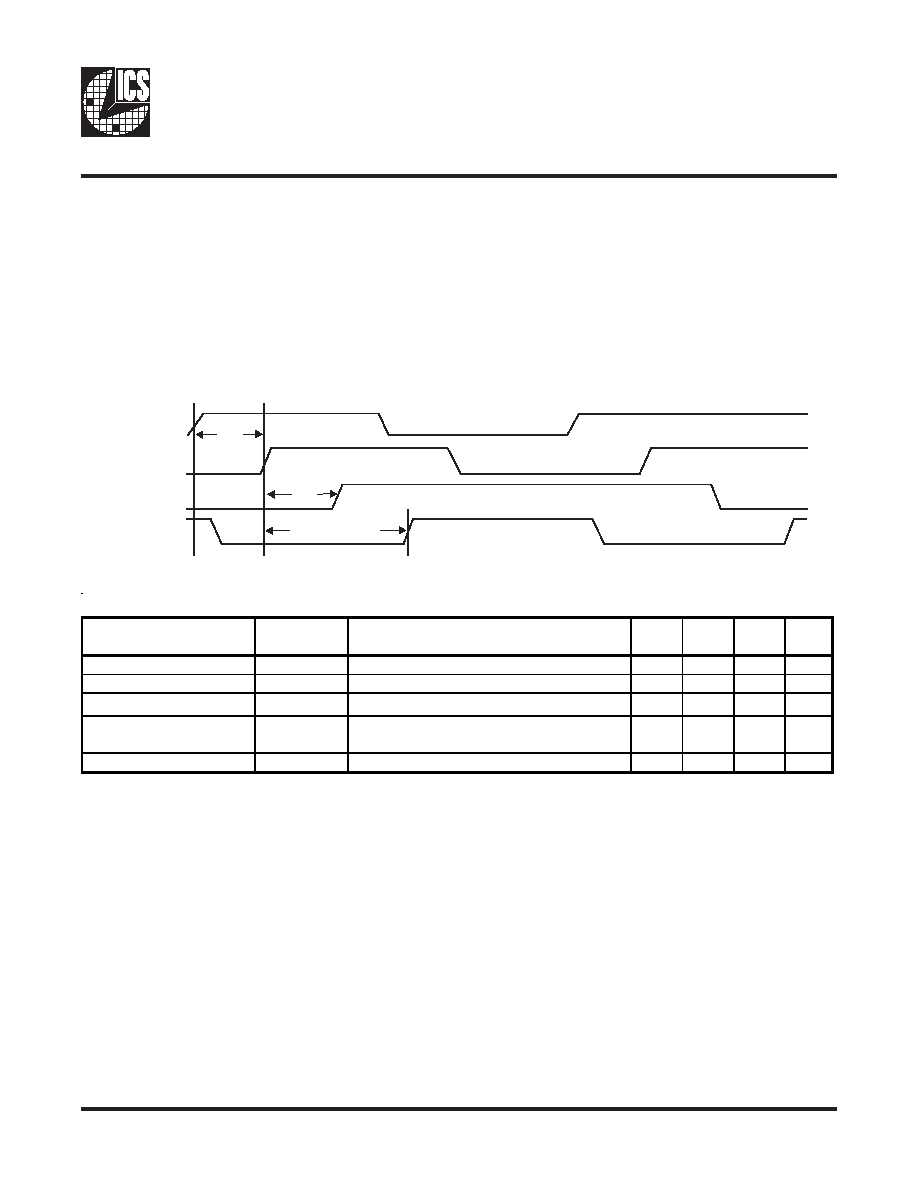
The impact of asserting the PCI_STOP# signal will be the following. All PCI[6:0] and stoppable PCI_F[2,0] clocks will
latch low in their next high to low transition.
PCI_STOP#
PCI_F[2:0] 33MHz
PCI[6:0] 33MHz
Assertion of PCI_STOP# Waveforms
PCI_STOP# - Assertion (transition from logic "1" to logic "0")
15
ICS932S203
0601E--12/22/04
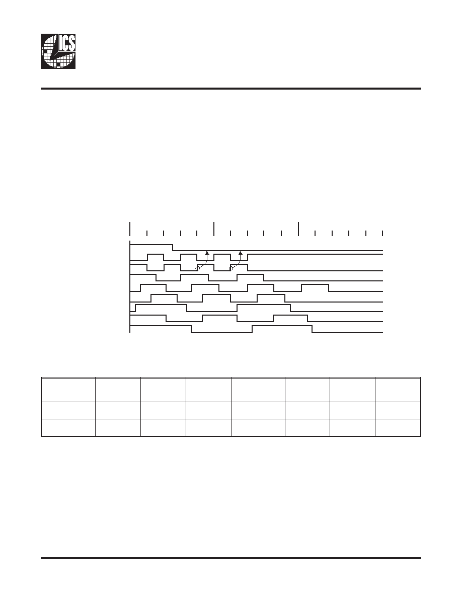
When PD# is sampled low by two consecutive rising edges of CPU clock then all clock outputs except CPU clocks
must be held low on their next high to low transition. CPU clocks must be held with the CPU clock pin driven high with
a value of 2x Iref, and CPUC undriven. Note the example below shows CPU = 100MHz, this diagram and description
is applicable for all valid CPU frequencies 66, 100, 133, 200MHz.
Due to the state of the internal logic, stopping and holding the REF clock outputs in the LOW state may require more
than one clock cycle to complete.
PD# - Assertion (transition from logic "1" to logic "0")
PD# Functionality
#
P
O
T
S
_
U
P
C
T
U
P
C
C
U
P
C
6
6
V
3
T
U
O
_
z
H
M
6
6
F
_
K
L
C
I
C
P
K
L
C
I
C
P
K
L
C
I
C
P
T
O
D
/
B
S
U
z
H
M
8
4
1
l
a
m
r
o
N
l
a
m
r
o
N
z
H
M
6
6
N
I
_
z
H
M
6
6
N
I
_
z
H
M
6
6
N
I
_
z
H
M
6
6
z
H
M
8
4
0
t
l
u
M
*
f
e
r
i
t
a
o
l
F
w
o
L
w
o
L
w
o
L
w
o
L
w
o
L
Power Down Assertion of Waveforms - Buffered Mode
0ns
PD#
CPUT 100MHz
CPUC 100MHz
3V66MHz
66MHz_IN
66MHz_OUT
PCI 33MHz
USB 48MHz
REF 14.318MHz
25ns
50ns
16
ICS932S203
0601E--12/22/04
MIN
MAX
MIN
MAX
A
2.413
2.794
.095
.110
A1
0.203
0.406
.008
.016
b
0.203
0.343
.008
.0135
c
0.127
0.254
.005
.010
D
E
10.033
10.668
.395
.420
E1
7.391
7.595
.291
.299
e
0.635 BASIC
0.025 BASIC
h
0.381
0.635
.015
.025
L
0.508
1.016
.020
.040
N
0∞
8∞
0∞
8∞
VARIATIONS
MIN
MAX
MIN
MAX
56
18.288
18.542
.720
.730
JEDEC MO-118
DOC# 10-0034
6/1/00
REV B
N
D mm.
D (inch)
SEE VARIATIONS
SYMBOL
SEE VARIATIONS
SEE VARIATIONS
In Millimeters
COMMON DIMENSIONS
In Inches
COMMON DIMENSIONS
SEE VARIATIONS
INDEX
AREA
INDEX
AREA
1 2
1 2
N
D
h x 45∞
h x 45∞
E1
E
SEATING
PLANE
SEATING
PLANE
A1
A
e
- C -
- C -
b
.10 (.004) C
.10 (.004) C
c
L
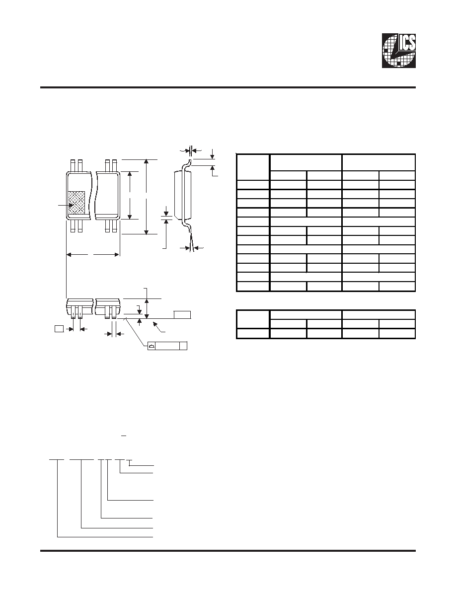
300 mil SSOP
Ordering Information
ICS932S203yFLFT
Example:
Designation for tape and reel packaging
Lead Option (optional)
LF = Lead Free
LN = Lead Free Annealed
Package Type
F = SSOP
Revision Designator (will not correlate with datasheet revision)
Device Type (consists of 3 or 4 digit numbers)
Prefix
ICS, AV = Standard Device
ICS XXXX y F Lx T

17
ICS932S203
0601E--12/22/04
6.10 mm. Body, 0.50 mm. pitch TSSOP
(240 mil)
(0.020 mil)
MIN
MAX
MIN
MAX
A
-
1.20
-
.047
A1
0.05
0.15
.002
.006
A2
0.80
1.05
.032
.041
b
0.17
0.27
.007
.011
c
0.09
0.20
.0035
.008
D
E
E1
6.00
6.20
.236
.244
e
0.50 BASIC
0.020 BASIC
L
0.45
0.75
.018
.30
N
0∞
8∞
0∞
8∞
aaa
-
0.10
-
.004
VARIATIONS
MIN
MAX
MIN
MAX
56
13.90
14.10
.547
.555
MO-153 JEDEC
Doc.# 10-0039
7/6/00 Rev B
SYMBOL
SEE VARIATIONS
SEE VARIATIONS
In Millimeters
COMMON DIMENSIONS
In Inches
COMMON DIMENSIONS
SEE VARIATIONS
8.10 BASIC
0.319
N
D mm.
D (inch)
SEE VARIATIONS
INDEX
AREA
INDEX
AREA
1 2
1 2
N
D
E1
E
a
SEATING
PLANE
SEATING
PLANE
A1
A
A2
A2
e
- C -
- C -
b
c
L
aaa
C
Ordering Information
ICS932S203yGLFT
Example:
Designation for tape and reel packaging
Lead Option (optional)
LF = Lead Free
LN = Lead Free Annealed
Package Type
G = TSSOP
Revision Designator (will not correlate with datasheet revision)
Device Type (consists of 3 or 4 digit numbers)
Prefix
ICS, AV = Standard Device
ICS XXXX y G Lx T