Document Outline
- General Description
- Features
- Block Diagram
- Pin Assignment
- Pin Descriptions
- Pin Characteristics
- Control Input Function Table
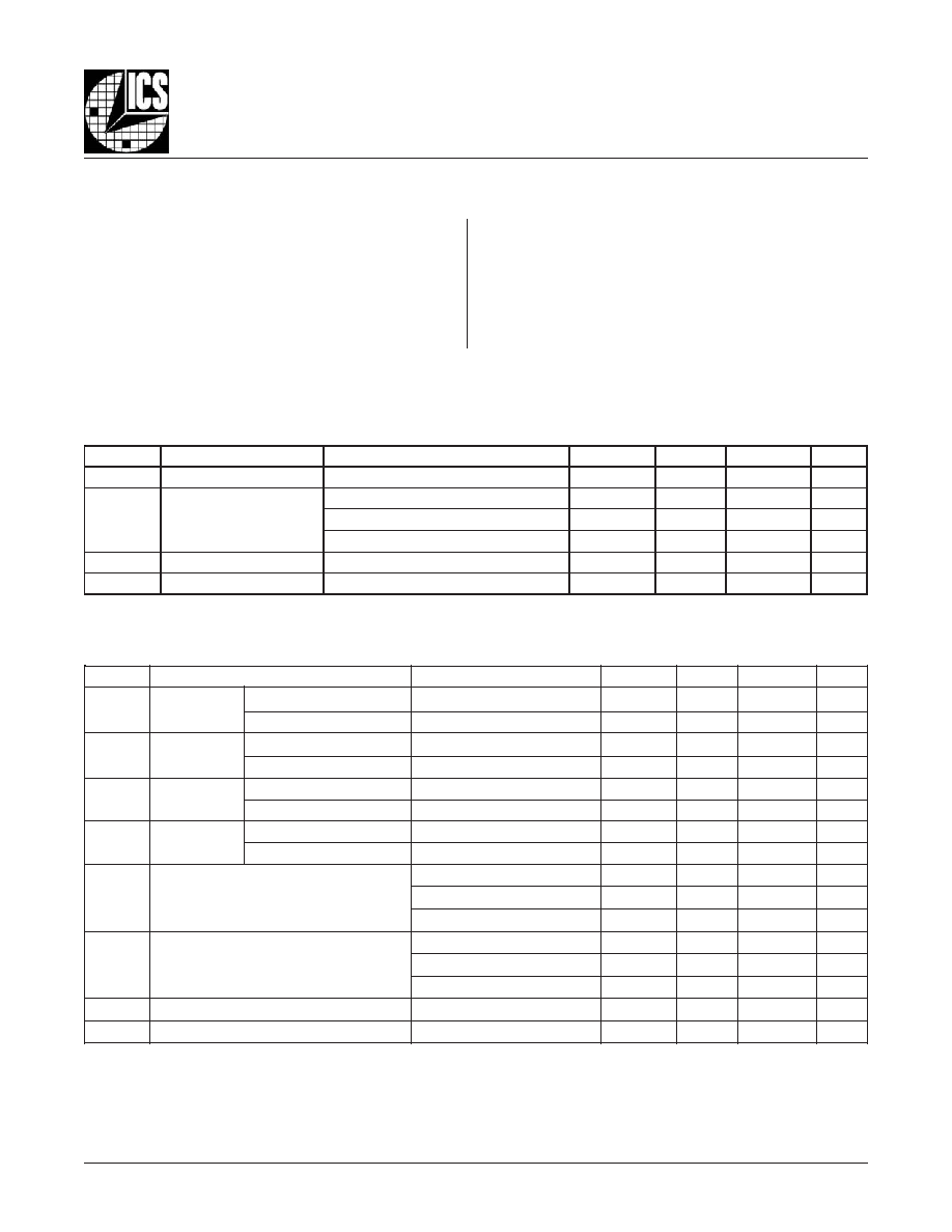
- CLK_EN Timing Diagram
- Absolute Maximum Ratings
- Power Supply 3.3V DC Characteristics
- LVCMOS 3.3V DC Characteristics
- Differential 3.3V DC Characteristics
- 3.3V AC Characteristics
- 3.3V/2.5V DC Characteristics
- 3.3V/1.8V DC Characteristics
- Additive Phase Jitter Plot
- Parameter Measurement Information
- 3.3V Core/3.3V Output Load AC Test Circuit Diagram
- 3.3V Core/2.5V Output Load AC Test Circuit Diagram
- 3.3V Core/1.8V Output Load AC Test Circuit Diagram
- Differential Input Levels Diagram
- Output Skew Diagram
- Part-to-Part Skew Diagram
- Propagation Delay Diagram
- Output Rise/Fall Time Diagram
- odc & tPeriod Diagram
- Application Information
- Wiring the Differential Input to Accept Single Ended Levels
- Single Ended Signal Driving Differential Input Diagram
- Differential Clock Input Interface
- HiPerClockS CLK/nCLK Input Driven by ICS HiPerClockS LVHSTL Driver Diagram
- HiPerClockS CLK/nCLK Input Driven by 3.3V LVPECL Driver Diagrams
- HiPerClockS CLK/nCLK Input Driven by 3.3V LVDS Driver Diagram
- HiPerClockS CLK/nCLK Input Driven by 3.3V LVPECL Driver w/AC Couple Diagram
- Schematic Example
- Reliability Information
- Transistor Count
- Package Outline
- Package Dimensions
- Ordering Information
- Revision History Sheet

Integrated
Circuit
Systems, Inc.
8305AG
www.icst.com/products/hiperclocks.html
REV. B FEBRUARY 26, 2004
1
ICS8305
L
OW
S
KEW
, 1-
TO
-4, M
ULTIPLEXED
D
IFFERENTIAL
/
LVCMOS-
TO
-LVCMOS/LVTTL F
ANOUT
B
UFFER
G
ENERAL
D
ESCRIPTION
The ICS8305 is a low skew, 1-to-4, Differential/
LVCMOS-to-LVCMOS/LVTTL Fanout Buffer and a
member of the HiPerClockS TM family of High
Performance Clock Solutions from ICS. The
ICS8305 has selectable clock inputs that accept
either differential or single ended input levels. The clock enable is
internally synchronized to eliminate runt pulses on the outputs
during asynchronous assertion/deassertion of the clock enable
pin. Outputs are forced LOW when the clock is disabled. A sepa-
rate output enable pin controls whether the outputs are in the
active or high impedance state.
Guaranteed output and part-to-part skew characteristics make
the ICS8305 ideal for those applications demanding well de-
fined performance and repeatability.
HiPerClockSTM
ICS
B
LOCK
D
IAGRAM
P
IN
A
SSIGNMENT
GND
OE
V
DD
CLK_EN
CLK
nCLK
CLK_SEL
LVCMOS_CLK
1
2
3
4
5
6
7
8
16
15
14
13
12
11
10
9
Q0
V
DDO
Q1
GND
Q2
V
DDO
Q3
GND
ICS8305
16-Lead TSSOP
4.4mm x 3.0mm x 0.92mm package body
G Package
Top View
F
EATURES
� 4 LVCMOS/LVTTL outputs
� Selectable differential or LVCMOS/LVTTL clock inputs
� CLK, nCLK pair can accept the following differential
input levels: LVPECL, LVDS, LVHSTL, HCSL, SSTL
� LVCMOS_CLK supports the following input types:
LVCMOS, LVTTL
� Maximum output frequency: 350MHz
� Output skew: 35ps (maximum)
� Part-to-part skew: 700ps (maximum)
� Additive phase jitter, RMS: 0.04ps (typical)
� 3.3V core, 3.3V, 2.5V or 1.8V output operating supply
� 0�C to 70�C ambient operating temperature
� Industrial temperature information available upon request
LVCMOS_CLK
CLK
nCLK
CLK_SEL
Q0
Q1
Q2
Q3
0
1
CLK_EN
OE
D
Q
LE
0
1

Integrated
Circuit
Systems, Inc.
8305AG
www.icst.com/products/hiperclocks.html
REV. B FEBRUARY 26, 2004
2
ICS8305
L
OW
S
KEW
, 1-
TO
-4, M
ULTIPLEXED
D
IFFERENTIAL
/
LVCMOS-
TO
-LVCMOS/LVTTL F
ANOUT
B
UFFER
T
ABLE
1. P
IN
D
ESCRIPTIONS
T
ABLE
2. P
IN
C
HARACTERISTICS
l
o
b
m
y
S
r
e
t
e
m
a
r
a
P
s
n
o
i
t
i
d
n
o
C
t
s
e
T
m
u
m
i
n
i
M
l
a
c
i
p
y
T
m
u
m
i
x
a
M
s
t
i
n
U
C
N
I
e
c
n
a
t
i
c
a
p
a
C
t
u
p
n
I
4
F
p
R
P
U
L
L
U
P
r
o
t
s
i
s
e
R
p
u
ll
u
P
t
u
p
n
I
1
5
K
R
N
W
O
D
L
L
U
P
r
o
t
s
i
s
e
R
n
w
o
d
ll
u
P
t
u
p
n
I
1
5
K
C
D
P
e
c
n
a
t
i
c
a
p
a
C
n
o
i
t
a
p
i
s
s
i
D
r
e
w
o
P
)
t
u
p
t
u
o
r
e
p
(
1
1
F
p
R
T
U
O
e
c
n
a
d
e
p
m
I
t
u
p
t
u
O
7
r
e
b
m
u
N
e
m
a
N
e
p
y
T
n
o
i
t
p
i
r
c
s
e
D
3
1
,
9
,
1
D
N
G
r
e
w
o
P
.
d
n
u
o
r
g
y
l
p
p
u
s
r
e
w
o
P
2
E
O
t
u
p
n
I
p
u
ll
u
P
.
e
t
a
t
s
e
c
n
a
d
e
p
m
i
H
G
I
H
n
i
e
r
a
s
t
u
p
t
u
o
,
W
O
L
n
e
h
W
.
e
l
b
a
n
e
t
u
p
t
u
O
.
s
l
e
v
e
l
e
c
a
f
r
e
t
n
i
L
T
T
V
L
/
S
O
M
C
V
L
.
e
v
i
t
c
a
e
r
a
s
t
u
p
t
u
o
,
H
G
I
H
n
e
h
W
3
V
D
D
r
e
w
o
P
.
n
i
p
y
l
p
p
u
s
e
r
o
C
4
N
E
_
K
L
C
t
u
p
n
I
p
u
ll
u
P
s
t
u
p
t
u
o
,
d
e
l
b
a
s
i
d
s
i
k
c
o
l
c
e
h
t
n
e
h
W
.
e
l
b
a
n
e
k
c
o
l
c
g
n
i
z
i
n
o
r
h
c
n
y
S
.
H
G
I
H
d
e
c
r
o
f
e
r
a
s
t
u
p
t
u
o
,
d
e
l
b
a
n
e
s
i
k
c
o
l
c
n
e
h
W
.
W
O
L
d
e
c
r
o
f
e
r
a
.
s
l
e
v
e
l
e
c
a
f
r
e
t
n
i
L
T
T
V
L
/
S
O
M
C
V
L
5
K
L
C
t
u
p
n
I
n
w
o
d
ll
u
P
.
t
u
p
n
i
k
c
o
l
c
l
a
i
t
n
e
r
e
f
f
i
d
g
n
i
t
r
e
v
n
i
-
n
o
N
6
K
L
C
n
t
u
p
n
I
/
p
u
ll
u
P
n
w
o
d
ll
u
P
V
.
t
u
p
n
i
k
c
o
l
c
l
a
i
t
n
e
r
e
f
f
i
d
g
n
i
t
r
e
v
n
I
D
D
.
g
n
i
t
a
o
l
f
t
f
e
l
n
e
h
w
t
l
u
a
f
e
d
2
/
7
L
E
S
_
K
L
C
t
u
p
n
I
p
u
ll
u
P
.
s
t
u
p
n
i
K
L
C
n
,
K
L
C
s
t
c
e
l
e
s
,
H
G
I
H
n
e
h
W
.
t
u
p
n
i
t
c
e
l
e
s
k
c
o
l
C
.
t
u
p
n
i
K
L
C
_
S
O
M
C
V
L
s
t
c
e
l
e
s
,
W
O
L
n
e
h
W
.
s
l
e
v
e
l
e
c
a
f
r
e
t
n
i
L
T
T
V
L
/
S
O
M
C
V
L
8
K
L
C
_
S
O
M
C
V
L
t
u
p
n
I
n
w
o
d
ll
u
P
.
t
u
p
n
i
k
c
o
l
c
L
T
T
V
L
/
S
O
M
C
V
L
6
1
,
4
1
,
2
1
,
0
1
0
Q
,
1
Q
,
2
Q
,
3
Q
t
u
p
t
u
O
.
s
l
e
v
e
l
e
c
a
f
r
e
t
n
i
L
T
T
V
L
/
S
O
M
C
V
L
.
s
t
u
p
t
u
o
k
c
o
l
C
5
1
,
1
1
V
O
D
D
r
e
w
o
P
.
s
n
i
p
y
l
p
p
u
s
t
u
p
t
u
O
:
E
T
O
N
p
u
ll
u
P
d
n
a
n
w
o
d
ll
u
P
.
s
e
u
l
a
v
l
a
c
i
p
y
t
r
o
f
,
s
c
i
t
s
i
r
e
t
c
a
r
a
h
C
n
i
P
,
2
e
l
b
a
T
e
e
S
.
s
r
o
t
s
i
s
e
r
t
u
p
n
i
l
a
n
r
e
t
n
i
o
t
r
e
f
e
r

Integrated
Circuit
Systems, Inc.
8305AG
www.icst.com/products/hiperclocks.html
REV. B FEBRUARY 26, 2004
3
ICS8305
L
OW
S
KEW
, 1-
TO
-4, M
ULTIPLEXED
D
IFFERENTIAL
/
LVCMOS-
TO
-LVCMOS/LVTTL F
ANOUT
B
UFFER
T
ABLE
3A. C
ONTROL
I
NPUT
F
UNCTION
T
ABLE
s
t
u
p
n
I
s
t
u
p
t
u
O
E
O
N
E
_
K
L
C
L
E
S
_
K
L
C
e
c
r
u
o
S
d
e
t
c
e
l
e
S
3
Q
:
0
Q
1
0
0
K
L
C
_
S
O
M
C
V
L
W
O
L
;
d
e
l
b
a
s
i
D
1
0
1
K
L
C
n
,
K
L
C
W
O
L
;
d
e
l
b
a
s
i
D
1
1
0
K
L
C
_
S
O
M
C
V
L
d
e
l
b
a
n
E
1
1
1
K
L
C
n
,
K
L
C
d
e
l
b
a
n
E
0
X
X
Z
i
H
e
g
d
e
k
c
o
l
c
t
u
p
n
i
g
n
il
l
a
f
d
n
a
g
n
i
s
i
r
a
g
n
i
w
o
ll
o
f
d
e
l
b
a
n
e
r
o
d
e
l
b
a
s
i
d
e
r
a
s
t
u
p
t
u
o
k
c
o
l
c
e
h
t
,
s
e
h
c
t
i
w
s
N
E
_
K
L
C
r
e
t
f
A
:
E
T
O
N
.
1
e
r
u
g
i
F
n
i
n
w
o
h
s
s
a
n
i
d
e
b
i
r
c
s
e
d
s
a
s
t
u
p
n
i
K
L
C
n
,
K
L
C
d
n
a
K
L
C
_
S
O
M
C
V
L
e
h
t
f
o
n
o
i
t
c
n
u
f
a
e
r
a
s
t
u
p
t
u
o
e
h
t
f
o
e
t
a
t
s
e
h
t
,
e
d
o
m
e
v
i
t
c
a
e
h
t
n
I
.
B
3
e
l
b
a
T
F
IGURE
1. CLK_EN T
IMING
D
IAGRAM
Enabled
Disabled
nCLK
CLK,
LVCMOS_CLK
CLK_EN
Q0:Q3
Integrated
Circuit
Systems, Inc.
8305AG
www.icst.com/products/hiperclocks.html
REV. B FEBRUARY 26, 2004
4
ICS8305
L
OW
S
KEW
, 1-
TO
-4, M
ULTIPLEXED
D
IFFERENTIAL
/
LVCMOS-
TO
-LVCMOS/LVTTL F
ANOUT
B
UFFER
T
ABLE
4A. P
OWER
S
UPPLY
DC C
HARACTERISTICS
,
V
DD
= 3.3V�5%, T
A
= 0�C
TO
70�C
l
o
b
m
y
S
r
e
t
e
m
a
r
a
P
s
n
o
i
t
i
d
n
o
C
t
s
e
T
m
u
m
i
n
i
M
l
a
c
i
p
y
T
m
u
m
i
x
a
M
s
t
i
n
U
V
D
D
e
g
a
t
l
o
V
y
l
p
p
u
S
e
r
o
C
5
3
1
.
3
3
.
3
5
6
4
.
3
V
V
O
D
D
e
g
a
t
l
o
V
y
l
p
p
u
S
t
u
p
t
u
O
5
3
1
.
3
3
.
3
5
6
4
.
3
V
5
7
3
.
2
5
.
2
5
2
6
.
2
V
5
6
.
1
8
.
1
5
9
.
1
V
I
D
D
t
n
e
r
r
u
C
y
l
p
p
u
S
r
e
w
o
P
1
2
A
m
I
O
D
D
t
n
e
r
r
u
C
y
l
p
p
u
S
t
u
p
t
u
O
5
A
m
l
o
b
m
y
S
r
e
t
e
m
a
r
a
P
s
n
o
i
t
i
d
n
o
C
t
s
e
T
m
u
m
i
n
i
M
l
a
c
i
p
y
T
m
u
m
i
x
a
M
s
t
i
n
U
V
H
I
t
u
p
n
I
e
g
a
t
l
o
V
h
g
i
H
E
O
,
L
E
S
_
K
L
C
,
N
E
_
K
L
C
2
V
D
D
3
.
0
+
V
K
L
C
_
S
O
M
C
V
L
2
V
D
D
3
.
0
+
V
V
L
I
t
u
p
n
I
e
g
a
t
l
o
V
w
o
L
E
O
,
L
E
S
_
K
L
C
,
N
E
_
K
L
C
3
.
0
-
8
.
0
V
K
L
C
_
S
O
M
C
V
L
3
.
0
-
3
.
1
V
I
H
I
t
u
p
n
I
t
n
e
r
r
u
C
h
g
i
H
E
O
,
L
E
S
_
K
L
C
,
N
E
_
K
L
C
V
D
D
V
=
N
I
V
5
6
4
.
3
=
5
A
�
K
L
C
_
S
O
M
C
V
L
V
D
D
V
=
N
I
V
5
6
4
.
3
=
0
5
1
A
�
I
L
I
t
u
p
n
I
t
n
e
r
r
u
C
w
o
L
E
O
,
L
E
S
_
K
L
C
,
N
E
_
K
L
C
V
D
D
V
,
V
5
6
4
.
3
=
N
I
V
0
=
0
5
1
-
A
�
K
L
C
_
S
O
M
C
V
L
V
D
D
V
,
V
5
6
4
.
3
=
N
I
V
0
=
5
-
A
�
V
H
O
1
E
T
O
N
;
e
g
a
t
l
o
V
h
g
i
H
t
u
p
t
u
O
V
O
D
D
%
5
�
V
3
.
3
=
6
.
2
V
V
O
D
D
%
5
�
V
5
.
2
=
8
.
1
V
V
O
D
D
V
5
1
.
0
�
V
8
.
1
=
5
.
1
V
V
L
O
1
E
T
O
N
;
e
g
a
t
l
o
V
w
o
L
t
u
p
t
u
O
V
O
D
D
%
5
�
V
3
.
3
=
5
.
0
V
V
O
D
D
%
5
�
V
5
.
2
=
5
.
0
V
V
O
D
D
V
5
1
.
0
�
V
8
.
1
=
4
.
0
V
I
L
Z
O
w
o
L
t
n
e
r
r
u
C
e
t
a
t
s
i
r
T
t
u
p
t
u
O
5
-
A
�
I
H
Z
O
h
g
i
H
t
n
e
r
r
u
C
e
t
a
t
s
i
r
T
t
u
p
t
u
O
5
A
�
0
5
h
t
i
w
d
e
t
a
n
i
m
r
e
t
s
t
u
p
t
u
O
:
1
E
T
O
N
V
o
t
O
D
D
.
t
i
u
c
r
i
C
t
s
e
T
d
a
o
L
t
u
p
t
u
O
,
n
o
i
t
a
m
r
o
f
n
I
t
n
e
m
e
r
u
s
a
e
M
r
e
t
e
m
a
r
a
P
e
e
S
.
2
/
T
ABLE
4B. LVCMOS/LVTTL DC C
HARACTERISTICS
,
V
DD
= 3.3V�5%, T
A
= 0�C
TO
70�C
A
BSOLUTE
M
AXIMUM
R
ATINGS
Supply Voltage, V
DD
4.6V
Inputs, V
I
-0.5V to V
DD
+ 0.5 V
Outputs, V
O
-0.5V to V
DD
+ 0.5V
Package Thermal Impedance,
JA
89�C/W (0 lfpm)
Storage Temperature, T
STG
-65�C to 150�C
NOTE: Stresses beyond those listed under Absolute
Maximum Ratings may cause permanent damage to the
device. These ratings are stress specifications only. Functional
operation of product at these conditions or any conditions be-
yond those listed in the
DC Characteristics or AC Character-
istics is not implied. Exposure to absolute maximum rating
conditions for extended periods may affect product reliability.
Integrated
Circuit
Systems, Inc.
8305AG
www.icst.com/products/hiperclocks.html
REV. B FEBRUARY 26, 2004
5
ICS8305
L
OW
S
KEW
, 1-
TO
-4, M
ULTIPLEXED
D
IFFERENTIAL
/
LVCMOS-
TO
-LVCMOS/LVTTL F
ANOUT
B
UFFER
T
ABLE
4C. D
IFFERENTIAL
DC C
HARACTERISTICS
,
V
DD
= 3.3V�5%, T
A
= 0�C
TO
70�C
l
o
b
m
y
S
r
e
t
e
m
a
r
a
P
s
n
o
i
t
i
d
n
o
C
t
s
e
T
m
u
m
i
n
i
M
l
a
c
i
p
y
T
m
u
m
i
x
a
M
s
t
i
n
U
I
H
I
t
n
e
r
r
u
C
h
g
i
H
t
u
p
n
I
K
L
C
n
V
N
I
V
=
D
D
V
5
6
4
.
3
=
0
5
1
A
�
K
L
C
V
N
I
V
=
D
D
V
5
6
4
.
3
=
0
5
1
A
�
I
L
I
t
n
e
r
r
u
C
w
o
L
t
u
p
n
I
K
L
C
n
V
N
I
V
,
V
0
=
D
D
V
5
6
4
.
3
=
0
5
1
-
A
�
K
L
C
V
N
I
V
,
V
0
=
D
D
V
5
6
4
.
3
=
5
-
A
�
V
P
P
e
g
a
t
l
o
V
t
u
p
n
I
k
a
e
P
-
o
t
-
k
a
e
P
5
1
.
0
3
.
1
V
V
R
M
C
;
e
g
a
t
l
o
V
t
u
p
n
I
e
d
o
M
n
o
m
m
o
C
2
,
1
E
T
O
N
5
.
0
+
D
N
G
V
D
D
5
8
.
0
-
V
s
n
o
i
t
a
c
il
p
p
a
d
e
d
n
e
e
l
g
n
i
s
r
o
F
:
1
E
T
O
N
,
V
s
i
K
L
C
n
,
K
L
C
r
o
f
e
g
a
t
l
o
v
t
u
p
n
i
m
u
m
i
x
a
m
e
h
t
D
D
.
V
3
.
0
+
V
s
a
d
e
n
i
f
e
d
s
i
e
g
a
t
l
o
v
e
d
o
m
n
o
m
m
o
C
:
2
E
T
O
N
H
I
.
T
ABLE
5A. AC C
HARACTERISTICS
,
V
DD
= V
DDO
= 3.3V � 5%, T
A
= 0�C
TO
70�C
l
o
b
m
y
S
r
e
t
e
m
a
r
a
P
s
n
o
i
t
i
d
n
o
C
t
s
e
T
m
u
m
i
n
i
M
l
a
c
i
p
y
T
m
u
m
i
x
a
M
s
t
i
n
U
f
X
A
M
y
c
n
e
u
q
e
r
F
t
u
p
t
u
O
0
5
3
z
H
M
p
t
H
L
,
y
a
l
e
D
n
o
i
t
a
g
a
p
o
r
P
h
g
i
H
o
t
w
o
L
;
K
L
C
_
S
O
M
C
V
L
A
1
E
T
O
N
;
K
L
C
n
,
K
L
C
B
1
E
T
O
N
5
7
.
1
5
7
.
2
s
n
t
)
o
(
k
s
6
,
2
E
T
O
N
;
w
e
k
S
t
u
p
t
u
O
e
g
d
E
g
n
i
s
i
R
e
h
t
n
o
d
e
r
u
s
a
e
M
5
3
s
p
t
)
p
p
(
k
s
6
,
3
E
T
O
N
;
w
e
k
S
t
r
a
P
-
o
t
-
t
r
a
P
0
0
7
s
p
t t
ij
;
S
M
R
,
r
e
t
t
i
J
e
s
a
h
P
e
v
i
t
i
d
d
A
r
e
f
f
u
B
,
n
o
i
t
c
e
S
r
e
t
t
i
J
e
s
a
h
P
e
v
i
t
i
d
d
A
o
t
r
e
f
e
r
5
E
T
O
N
4
0
.
0
s
p
t
R
t
/
F
4
E
T
O
N
;
e
m
i
T
ll
a
F
/
e
s
i
R
t
u
p
t
u
O
%
0
8
o
t
%
0
2
0
0
1
0
0
7
s
p
c
d
o
e
l
c
y
C
y
t
u
D
t
u
p
t
u
O
K
L
C
n
/
K
L
C
=
f
e
R
5
4
5
5
%
,
K
L
C
_
S
O
M
C
V
L
=
f
e
R
z
H
M
0
0
3
5
4
5
5
%
t
N
E
4
E
T
O
N
;
e
m
i
T
e
l
b
a
n
E
t
u
p
t
u
O
5
s
n
t
S
I
D
4
E
T
O
N
;
e
m
i
T
e
l
b
a
s
i
D
t
u
p
t
u
O
5
s
n
t
a
d
e
r
u
s
a
e
m
s
r
e
t
e
m
a
r
a
p
ll
A
z
H
M
0
5
3
.
e
s
i
w
r
e
h
t
o
d
e
t
o
n
s
s
e
l
n
u
V
e
h
t
m
o
r
f
d
e
r
u
s
a
e
M
:
A
1
E
T
O
N
D
D
V
o
t
t
u
p
n
i
e
h
t
f
o
2
/
O
D
D
.
t
u
p
t
u
o
e
h
t
f
o
2
/
V
o
t
t
n
i
o
p
g
n
i
s
s
o
r
c
t
u
p
n
i
l
a
i
t
n
e
r
e
f
f
i
d
e
h
t
m
o
r
f
d
e
r
u
s
a
e
M
:
B
1
E
T
O
N
O
D
D
.
t
u
p
t
u
o
e
h
t
f
o
2
/
.
s
n
o
i
t
i
d
n
o
c
d
a
o
l
l
a
u
q
e
h
t
i
w
d
n
a
e
g
a
t
l
o
v
y
l
p
p
u
s
e
m
a
s
e
h
t
t
a
s
t
u
p
t
u
o
n
e
e
w
t
e
b
w
e
k
s
s
a
d
e
n
i
f
e
D
:
2
E
T
O
N
V
t
a
d
e
r
u
s
a
e
M
O
D
D
.
2
/
d
n
a
s
e
g
a
t
l
o
v
y
l
p
p
u
s
e
m
a
s
e
h
t
a
g
n
i
t
a
r
e
p
o
s
e
c
i
v
e
d
t
n
e
r
e
f
f
i
d
n
o
s
t
u
p
t
u
o
n
e
e
w
t
e
b
w
e
k
s
s
a
d
e
n
i
f
e
D
:
3
E
T
O
N
V
t
a
d
e
r
u
s
a
e
m
s
i
t
u
p
t
u
o
e
h
t
,
e
c
i
v
e
d
h
c
a
e
n
o
t
u
p
n
i
f
o
e
p
y
t
e
m
a
s
e
h
t
g
n
i
s
U
.
s
n
o
i
t
i
d
n
o
c
d
a
o
l
l
a
u
q
e
h
t
i
w
O
D
D
.
2
/
.
n
o
i
t
c
u
d
o
r
p
n
i
d
e
t
s
e
t
t
o
N
.
n
o
i
t
a
z
i
r
e
t
c
a
r
a
h
c
y
b
d
e
e
t
n
a
r
a
u
g
e
r
a
s
r
e
t
e
m
a
r
a
p
e
s
e
h
T
:
4
E
T
O
N
.
k
c
o
l
c
t
u
p
n
i
e
n
o
y
l
n
o
g
n
i
v
i
r
D
:
5
E
T
O
N
.
5
6
d
r
a
d
n
a
t
S
C
E
D
E
J
h
t
i
w
e
c
n
a
d
r
o
c
c
a
n
i
d
e
n
i
f
e
d
s
i
r
e
t
e
m
a
r
a
p
s
i
h
T
:
6
E
T
O
N
Integrated
Circuit
Systems, Inc.
8305AG
www.icst.com/products/hiperclocks.html
REV. B FEBRUARY 26, 2004
6
ICS8305
L
OW
S
KEW
, 1-
TO
-4, M
ULTIPLEXED
D
IFFERENTIAL
/
LVCMOS-
TO
-LVCMOS/LVTTL F
ANOUT
B
UFFER
T
ABLE
5C. AC C
HARACTERISTICS
,
V
DD
= 3.3V � 5%, V
DDO
= 1.8V � -0.15V, T
A
= 0�C
TO
70�C
T
ABLE
5B. AC C
HARACTERISTICS
,
V
DD
= 3.3V � 5%, V
DDO
= 2.5V � 5%, T
A
= 0�C
TO
70�C
l
o
b
m
y
S
r
e
t
e
m
a
r
a
P
s
n
o
i
t
i
d
n
o
C
t
s
e
T
m
u
m
i
n
i
M
l
a
c
i
p
y
T
m
u
m
i
x
a
M
s
t
i
n
U
f
X
A
M
y
c
n
e
u
q
e
r
F
t
u
p
t
u
O
0
5
3
z
H
M
p
t
H
L
,
y
a
l
e
D
n
o
i
t
a
g
a
p
o
r
P
h
g
i
H
o
t
w
o
L
;
K
L
C
_
S
O
M
C
V
L
A
1
E
T
O
N
;
K
L
C
n
,
K
L
C
B
1
E
T
O
N
8
.
1
9
.
2
s
n
t
)
o
(
k
s
6
,
2
E
T
O
N
;
w
e
k
S
t
u
p
t
u
O
e
g
d
E
g
n
i
s
i
R
e
h
t
n
o
d
e
r
u
s
a
e
M
5
3
s
p
t
)
p
p
(
k
s
6
,
3
E
T
O
N
;
w
e
k
S
t
r
a
P
-
o
t
-
t
r
a
P
0
0
8
s
p
t
i
j
t
;
S
M
R
,
r
e
t
t
i
J
e
s
a
h
P
e
v
i
t
i
d
d
A
r
e
f
f
u
B
,
n
o
i
t
c
e
S
r
e
t
t
i
J
e
s
a
h
P
e
v
i
t
i
d
d
A
o
t
r
e
f
e
r
5
E
T
O
N
4
0
.
0
s
p
t
R
t
/
F
4
E
T
O
N
;
e
m
i
T
ll
a
F
/
e
s
i
R
t
u
p
t
u
O
%
0
8
o
t
%
0
2
0
0
1
0
0
7
s
p
c
d
o
e
l
c
y
C
y
t
u
D
t
u
p
t
u
O
K
L
C
n
/
K
L
C
=
f
e
R
4
4
6
5
%
,
K
L
C
_
S
O
M
C
V
L
=
f
e
R
z
H
M
0
0
3
4
4
6
5
%
t
N
E
4
E
T
O
N
;
e
m
i
T
e
l
b
a
n
E
t
u
p
t
u
O
5
s
n
t
S
I
D
4
E
T
O
N
;
e
m
i
T
e
l
b
a
s
i
D
t
u
p
t
u
O
5
s
n
t
a
d
e
r
u
s
a
e
m
s
r
e
t
e
m
a
r
a
p
ll
A
z
H
M
0
5
3
.
e
s
i
w
r
e
h
t
o
d
e
t
o
n
s
s
e
l
n
u
V
e
h
t
m
o
r
f
d
e
r
u
s
a
e
M
:
A
1
E
T
O
N
D
D
V
o
t
t
u
p
n
i
e
h
t
f
o
2
/
O
D
D
.
t
u
p
t
u
o
e
h
t
f
o
2
/
V
o
t
t
n
i
o
p
g
n
i
s
s
o
r
c
t
u
p
n
i
l
a
i
t
n
e
r
e
f
f
i
d
e
h
t
m
o
r
f
d
e
r
u
s
a
e
M
:
B
1
E
T
O
N
O
D
D
.
t
u
p
t
u
o
e
h
t
f
o
2
/
V
t
a
d
e
r
u
s
a
e
M
.
s
n
o
i
t
i
d
n
o
c
d
a
o
l
l
a
u
q
e
h
t
i
w
d
n
a
e
g
a
t
l
o
v
y
l
p
p
u
s
e
m
a
s
e
h
t
t
a
s
t
u
p
t
u
o
n
e
e
w
t
e
b
w
e
k
s
s
a
d
e
n
i
f
e
D
:
2
E
T
O
N
O
D
D
.
2
/
d
n
a
s
e
g
a
t
l
o
v
y
l
p
p
u
s
e
m
a
s
e
h
t
a
g
n
i
t
a
r
e
p
o
s
e
c
i
v
e
d
t
n
e
r
e
f
f
i
d
n
o
s
t
u
p
t
u
o
n
e
e
w
t
e
b
w
e
k
s
s
a
d
e
n
i
f
e
D
:
3
E
T
O
N
V
t
a
d
e
r
u
s
a
e
m
s
i
t
u
p
t
u
o
e
h
t
,
e
c
i
v
e
d
h
c
a
e
n
o
t
u
p
n
i
f
o
e
p
y
t
e
m
a
s
e
h
t
g
n
i
s
U
.
s
n
o
i
t
i
d
n
o
c
d
a
o
l
l
a
u
q
e
h
t
i
w
O
D
D
.
2
/
.
n
o
i
t
c
u
d
o
r
p
n
i
d
e
t
s
e
t
t
o
N
.
n
o
i
t
a
z
i
r
e
t
c
a
r
a
h
c
y
b
d
e
e
t
n
a
r
a
u
g
e
r
a
s
r
e
t
e
m
a
r
a
p
e
s
e
h
T
:
4
E
T
O
N
.
k
c
o
l
c
t
u
p
n
i
e
n
o
y
l
n
o
g
n
i
v
i
r
D
:
5
E
T
O
N
.
5
6
d
r
a
d
n
a
t
S
C
E
D
E
J
h
t
i
w
e
c
n
a
d
r
o
c
c
a
n
i
d
e
n
i
f
e
d
s
i
r
e
t
e
m
a
r
a
p
s
i
h
T
:
6
E
T
O
N
l
o
b
m
y
S
r
e
t
e
m
a
r
a
P
s
n
o
i
t
i
d
n
o
C
t
s
e
T
m
u
m
i
n
i
M
l
a
c
i
p
y
T
m
u
m
i
x
a
M
s
t
i
n
U
f
X
A
M
y
c
n
e
u
q
e
r
F
t
u
p
t
u
O
0
5
3
z
H
M
p
t
H
L
,
y
a
l
e
D
n
o
i
t
a
g
a
p
o
r
P
h
g
i
H
o
t
w
o
L
;
K
L
C
_
S
O
M
C
V
L
A
1
E
T
O
N
;
K
L
C
n
,
K
L
C
B
1
E
T
O
N
5
9
.
1
5
6
.
3
s
n
t
)
o
(
k
s
6
,
2
E
T
O
N
;
w
e
k
S
t
u
p
t
u
O
e
g
d
E
g
n
i
s
i
R
e
h
t
n
o
d
e
r
u
s
a
e
M
5
3
s
p
t
)
p
p
(
k
s
6
,
3
E
T
O
N
;
w
e
k
S
t
r
a
P
-
o
t
-
t
r
a
P
0
0
9
s
p
t
i
j
t
;
S
M
R
,
r
e
t
t
i
J
e
s
a
h
P
e
v
i
t
i
d
d
A
r
e
f
f
u
B
,
n
o
i
t
c
e
S
r
e
t
t
i
J
e
s
a
h
P
e
v
i
t
i
d
d
A
o
t
r
e
f
e
r
5
E
T
O
N
4
0
.
0
s
p
t
R
t
/
F
4
E
T
O
N
;
e
m
i
T
ll
a
F
/
e
s
i
R
t
u
p
t
u
O
%
0
8
o
t
%
0
2
0
0
1
0
0
7
s
p
c
d
o
e
l
c
y
C
y
t
u
D
t
u
p
t
u
O
K
L
C
n
/
K
L
C
=
f
e
R
4
4
6
5
%
,
K
L
C
_
S
O
M
C
V
L
=
f
e
R
z
H
M
0
0
3
4
4
6
5
%
t
N
E
4
E
T
O
N
;
e
m
i
T
e
l
b
a
n
E
t
u
p
t
u
O
5
s
n
t
S
I
D
4
E
T
O
N
;
e
m
i
T
e
l
b
a
s
i
D
t
u
p
t
u
O
5
s
n
.
B
5
e
l
b
a
T
n
i
s
e
t
o
n
e
e
S

Integrated
Circuit
Systems, Inc.
8305AG
www.icst.com/products/hiperclocks.html
REV. B FEBRUARY 26, 2004
7
ICS8305
L
OW
S
KEW
, 1-
TO
-4, M
ULTIPLEXED
D
IFFERENTIAL
/
LVCMOS-
TO
-LVCMOS/LVTTL F
ANOUT
B
UFFER
A
DDITIVE
P
HASE
J
ITTER
Input/Output Additive
Phase Jitter
at 155.52MHz
= 0.04ps typical
0
-10
-20
-30
-40
-50
-60
-70
-80
-90
-100
-110
-120
-130
-140
-150
-160
-170
-180
-190
100
1k
10k
100k
1M
10M
100M
The spectral purity in a band at a specific offset from the funda-
mental compared to the power of the fundamental is called the
dBc Phase Noise. This value is normally expressed using a
Phase noise plot and is most often the specified plot in many
applications. Phase noise is defined as the ratio of the noise
power present in a 1Hz band at a specified offset from the fun-
damental frequency to the power value of the fundamental. This
ratio is expressed in decibels (dBm) or a ratio of the power in
As with most timing specifications, phase noise measurements
have issues. The primary issue relates to the limitations of the
equipment. Often the noise floor of the equipment is higher than
the noise floor of the device. This is illustrated above. The de-
the 1Hz band to the power in the fundamental. When the re-
quired offset is specified, the phase noise is called a
dBc value,
which simply means dBm at a specified offset from the funda-
mental. By investigating jitter in the frequency domain, we get a
better understanding of its effects on the desired application over
the entire time record of the signal. It is mathematically possible
to calculate an expected bit error rate given a phase noise plot.
vice meets the noise floor of what is shown, but can actually be
lower. The phase noise is dependant on the input source and
measurement equipment.
O
FFSET
F
ROM
C
ARRIER
F
REQUENCY
(H
Z
)
SSB P
HASE
N
OISE
dBc/H
Z

Integrated
Circuit
Systems, Inc.
8305AG
www.icst.com/products/hiperclocks.html
REV. B FEBRUARY 26, 2004
8
ICS8305
L
OW
S
KEW
, 1-
TO
-4, M
ULTIPLEXED
D
IFFERENTIAL
/
LVCMOS-
TO
-LVCMOS/LVTTL F
ANOUT
B
UFFER
P
ARAMETER
M
EASUREMENT
I
NFORMATION
P
ART
-
TO
-P
ART
S
KEW
tsk(o)
V
DDO
2
V
DDO
2
Qx
Qy
D
IFFERENTIAL
I
NPUT
L
EVEL
O
UTPUT
S
KEW
3.3V C
ORE
/3.3V O
UTPUT
L
OAD
AC T
EST
C
IRCUIT
SCOPE
Qx
LVCMOS
V
CMR
Cross Points
V
PP
GND
CLK
nCLK
V
DD
tsk(pp)
V
DDO
2
V
DDO
2
Qx
Qy
PART 1
PART 2
-1.65V�5%
1.65V�5%
3.3V C
ORE
/2.5V O
UTPUT
L
OAD
AC T
EST
C
IRCUIT
3.3V C
ORE
/1.8V O
UTPUT
L
OAD
AC T
EST
C
IRCUIT
-1.25V�5%
1.25V�5%
SCOPE
Qx
LVCMOS
-0.9V�0.075V
0.9V�0.075V
V
DD
V
DDO
2.4V�0.09V
SCOPE
Qx
LVCMOS
V
DD
V
DDO
2.05V�5%
V
DD
,
V
DDO
GND
GND
GND
Integrated
Circuit
Systems, Inc.
8305AG
www.icst.com/products/hiperclocks.html
REV. B FEBRUARY 26, 2004
9
ICS8305
L
OW
S
KEW
, 1-
TO
-4, M
ULTIPLEXED
D
IFFERENTIAL
/
LVCMOS-
TO
-LVCMOS/LVTTL F
ANOUT
B
UFFER
P
ROPAGATION
D
ELAY
O
UTPUT
R
ISE
/F
ALL
T
IME
Clock
Outputs
20%
80%
80%
20%
t
R
t
F
nCLK
CLK
Q0:Q3
t
PD
V
DDO
2
V
DD
2
O
UTPUT
D
UTY
C
YCLE
/P
ULSE
W
IDTH
/P
ERIOD
Pulse Width
t
PERIOD
t
PW
t
PERIOD
odc =
V
DDO
2
Q0:Q3
LVCMOS_CLK

Integrated
Circuit
Systems, Inc.
8305AG
www.icst.com/products/hiperclocks.html
REV. B FEBRUARY 26, 2004
10
ICS8305
L
OW
S
KEW
, 1-
TO
-4, M
ULTIPLEXED
D
IFFERENTIAL
/
LVCMOS-
TO
-LVCMOS/LVTTL F
ANOUT
B
UFFER
A
PPLICATION
I
NFORMATION
F
IGURE
2. S
INGLE
E
NDED
S
IGNAL
D
RIVING
D
IFFERENTIAL
I
NPUT
Figure 2 shows how the differential input can be wired to accept
single ended levels. The reference voltage V_REF = V
DD
/2 is
generated by the bias resistors R1, R2 and C1. This bias circuit
should be located as close as possible to the input pin. The ratio
W
IRING
THE
D
IFFERENTIAL
I
NPUT
TO
A
CCEPT
S
INGLE
E
NDED
L
EVELS
of R1 and R2 might need to be adjusted to position the V_REF in
the center of the input voltage swing. For example, if the input
clock swing is only 2.5V and V
DD
= 3.3V, V_REF should be 1.25V
and R2/R1 = 0.609.
V_REF
R1
1K
C1
0.1u
R2
1K
Single Ended Clock Input
CLK
nCLK
VDD

Integrated
Circuit
Systems, Inc.
8305AG
www.icst.com/products/hiperclocks.html
REV. B FEBRUARY 26, 2004
11
ICS8305
L
OW
S
KEW
, 1-
TO
-4, M
ULTIPLEXED
D
IFFERENTIAL
/
LVCMOS-
TO
-LVCMOS/LVTTL F
ANOUT
B
UFFER
F
IGURE
3C. H
I
P
ER
C
LOCK
S CLK/nCLK I
NPUT
D
RIVEN
BY
3.3V LVPECL D
RIVER
F
IGURE
3B. H
I
P
ER
C
LOCK
S CLK/nCLK I
NPUT
D
RIVEN
BY
3.3V LVPECL D
RIVER
F
IGURE
3D. H
I
P
ER
C
LOCK
S CLK/nCLK I
NPUT
D
RIVEN
BY
3.3V LVDS D
RIVER
3.3V
R1
50
R3
50
Zo = 50 Ohm
LVPECL
Zo = 50 Ohm
HiPerClockS
CLK
nCLK
3.3V
Input
R2
50
Zo = 50 Ohm
Input
HiPerClockS
CLK
nCLK
3.3V
R3
125
R2
84
Zo = 50 Ohm
3.3V
R4
125
LVPECL
R1
84
3.3V
D
IFFERENTIAL
C
LOCK
I
NPUT
I
NTERFACE
The CLK /nCLK accepts LVDS, LVPECL, LVHSTL, SSTL, HCSL
and other differential signals. Both V
SWING
and V
OH
must meet the
V
PP
and V
CMR
input requirements. Figures 3A to 3E show inter-
face examples for the HiPerClockS CLK/nCLK input driven by
the most common driver types. The input interfaces suggested
F
IGURE
3A. H
I
P
ER
C
LOCK
S CLK/nCLK I
NPUT
D
RIVEN
BY
ICS H
I
P
ER
C
LOCK
S LVHSTL D
RIVER
here are examples only. Please consult with the vendor of the
driver component to confirm the driver termination requirements.
For example in
Figure 3A, the input termination applies for ICS
HiPerClockS LVHSTL drivers. If you are using an LVHSTL driver
from another vendor, use their termination recommendation.
1.8V
R2
50
Input
LVHSTL Driver
ICS
HiPerClockS
R1
50
LVHSTL
3.3V
Zo = 50 Ohm
Zo = 50 Ohm
HiPerClockS
CLK
nCLK
F
IGURE
3E. H
I
P
ER
C
LOCK
S CLK/nCLK I
NPUT
D
RIVEN
BY
3.3V LVPECL D
RIVER
WITH
AC C
OUPLE
Zo = 50 Ohm
R3
125
HiPerClockS
CLK
nCLK
3.3V
R5
100 - 200
3.3V
R2
84
3.3V
R6
100 - 200
Input
R5,R6 locate near the driver pin.
Zo = 50 Ohm
R1
84
R4
125
C2
LVPECL
C1
Zo = 50 Ohm
R1
100
3.3V
LVDS_Driv er
Zo = 50 Ohm
Receiv er
CLK
nCLK
3.3V

Integrated
Circuit
Systems, Inc.
8305AG
www.icst.com/products/hiperclocks.html
REV. B FEBRUARY 26, 2004
12
ICS8305
L
OW
S
KEW
, 1-
TO
-4, M
ULTIPLEXED
D
IFFERENTIAL
/
LVCMOS-
TO
-LVCMOS/LVTTL F
ANOUT
B
UFFER
LVCMOS Receiv er
R1
43
VDD
R5
1K
LVCMOS Receiv er
VDD=3.3V
VDD
R4
1K
Zo = 50
(U1,11)
Ro ~ 7 Ohm
3,.3V LVCMOS
(U1,15)
(U1,3)
VDD
R3
43
R2
43
C2
0.1u
U1
ICS8305
1
2
3
4
5
6
7
8
9
10
11
12
13
14
15
16
GND
OE
VDD
CLK_EN
CLK
nCLK
CLK_SEL
LVCMOS_CLK
GND
Q3
VDDO
Q2
GND
Q1
VDDO
Q0
Zo = 50
VDD
Zo = 50
C1
0.1u
R6
1K
C3
0.1u
S
CHEMATIC
E
XAMPLE
This application note provides general design guide using
ICS8305 LVCMOS buffer.
Figure 3 shows a schematic example
of the ICS8305 LVCMOS clock buffer. In this example, the input
F
IGURE
4. E
XAMPLE
ICS8305 LVCMOS C
LOCK
O
UTPUT
B
UFFER
S
CHEMATIC
is driven by an LVCMOS driver. CLK_EN is set at logic low to
select LVCMOS_CLK input.

Integrated
Circuit
Systems, Inc.
8305AG
www.icst.com/products/hiperclocks.html
REV. B FEBRUARY 26, 2004
13
ICS8305
L
OW
S
KEW
, 1-
TO
-4, M
ULTIPLEXED
D
IFFERENTIAL
/
LVCMOS-
TO
-LVCMOS/LVTTL F
ANOUT
B
UFFER
R
ELIABILITY
I
NFORMATION
T
RANSISTOR
C
OUNT
The transistor count for ICS8305 is: 459
T
ABLE
6.
JA
VS
. A
IR
F
LOW
T
ABLE
FOR
16 L
EAD
TSSOP
JA
by Velocity (Linear Feet per Minute)
0
200
500
Single-Layer PCB, JEDEC Standard Test Boards
137.1�C/W
118.2�C/W
106.8�C/W
Multi-Layer PCB, JEDEC Standard Test Boards
89.0�C/W
81.8�C/W
78.1�C/W
NOTE: Most modern PCB designs use multi-layered boards. The data in the second row pertains to most designs.
Integrated
Circuit
Systems, Inc.
8305AG
www.icst.com/products/hiperclocks.html
REV. B FEBRUARY 26, 2004
14
ICS8305
L
OW
S
KEW
, 1-
TO
-4, M
ULTIPLEXED
D
IFFERENTIAL
/
LVCMOS-
TO
-LVCMOS/LVTTL F
ANOUT
B
UFFER
P
ACKAGE
O
UTLINE
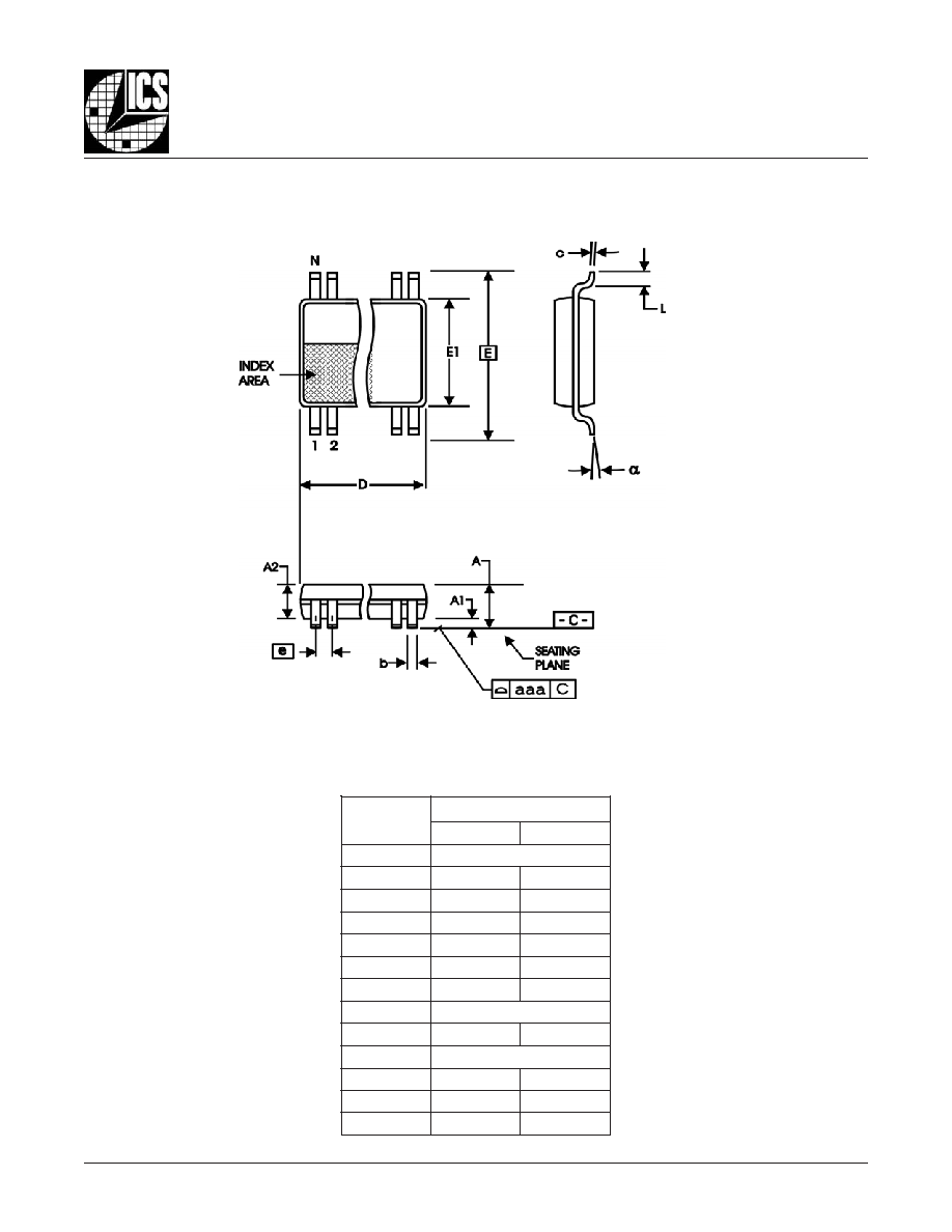
- G S
UFFIX
FOR
16 L
EAD
TSSOP
T
ABLE
7. P
ACKAGE
D
IMENSIONS
Reference Document: JEDEC Publication 95, MO-153
L
O
B
M
Y
S
s
r
e
t
e
m
i
l
l
i
M
m
u
m
i
n
i
M
m
u
m
i
x
a
M
N
6
1
A
-
-
0
2
.
1
1
A
5
0
.
0
5
1
.
0
2
A
0
8
.
0
5
0
.
1
b
9
1
.
0
0
3
.
0
c
9
0
.
0
0
2
.
0
D
0
9
.
4
0
1
.
5
E
C
I
S
A
B
0
4
.
6
1
E
0
3
.
4
0
5
.
4
e
C
I
S
A
B
5
6
.
0
L
5
4
.
0
5
7
.
0
�
0
�
8
a
a
a
-
-
0
1
.
0
Integrated
Circuit
Systems, Inc.
8305AG
www.icst.com/products/hiperclocks.html
REV. B FEBRUARY 26, 2004
15
ICS8305
L
OW
S
KEW
, 1-
TO
-4, M
ULTIPLEXED
D
IFFERENTIAL
/
LVCMOS-
TO
-LVCMOS/LVTTL F
ANOUT
B
UFFER
T
ABLE
8. O
RDERING
I
NFORMATION
While the information presented herein has been checked for both accuracy and reliability, Integrated Circuit Systems, Incorporated (ICS) assumes no responsibility for either its use
or for infringement of any patents or other rights of third parties, which would result from its use. No other circuits, patents, or licenses are implied. This product is intended for use
in normal commercial applications. Any other applications such as those requiring extended temperature range, high reliability, or other extraordinary environmental requirements are
not recommended without additional processing by ICS. ICS reserves the right to change any circuitry or specifications without notice. ICS does not authorize or warrant any ICS
product for use in life support devices or critical medical instruments.
r
e
b
m
u
N
r
e
d
r
O
/
t
r
a
P
g
n
i
k
r
a
M
e
g
a
k
c
a
P
t
n
u
o
C
e
r
u
t
a
r
e
p
m
e
T
G
A
5
0
3
8
S
C
I
G
A
5
0
3
8
S
C
I
P
O
S
S
T
d
a
e
L
6
1
e
b
u
t
r
e
p
4
9
C
�
0
7
o
t
C
�
0
T
G
A
5
0
3
8
S
C
I
G
A
5
0
3
8
S
C
I
l
e
e
R
d
n
a
e
p
a
T
n
o
P
O
S
S
T
d
a
e
L
6
1
0
0
5
2
C
�
0
7
o
t
C
�
0
Integrated
Circuit
Systems, Inc.
8305AG
www.icst.com/products/hiperclocks.html
REV. B FEBRUARY 26, 2004
16
ICS8305
L
OW
S
KEW
, 1-
TO
-4, M
ULTIPLEXED
D
IFFERENTIAL
/
LVCMOS-
TO
-LVCMOS/LVTTL F
ANOUT
B
UFFER
T
E
E
H
S
Y
R
O
T
S
I
H
N
O
I
S
I
V
E
R
v
e
R
e
l
b
a
T
e
g
a
P
e
g
n
a
h
C
f
o
n
o
i
t
p
i
r
c
s
e
D
e
t
a
D
A
8
T
4
1
m
o
r
f
o
p
y
t
r
e
b
m
u
N
r
e
d
r
O
/
t
r
a
P
d
e
t
c
e
r
r
o
c
-
e
l
b
a
t
n
o
i
t
a
m
r
o
f
n
I
g
n
i
r
e
d
r
O
.
T
G
A
5
0
3
8
S
C
I
o
t
T
G
A
5
0
3
8
8
S
C
I
4
0
/
0
2
/
1
B
C
5
T
-
A
5
T
6
&
5
7
.
s
e
l
b
a
T
s
c
i
t
s
i
r
e
t
c
a
r
a
h
C
C
A
o
t
r
e
t
t
i
J
e
s
a
h
P
e
v
i
t
i
d
d
A
d
e
d
d
A
.
n
o
i
t
c
e
S
r
e
t
t
i
J
e
s
a
h
P
e
v
i
t
i
d
d
A
d
e
d
d
A
4
0
/
6
2
/
2