Document Outline
- General Description
- Features
- Block Diagram
- Pin Assignment
- Pin Descriptions
- Pin Characteristics
- Output Enable & Clock Enable Function Table
- Clock Input Function Table
- Absolute Maximum Ratings
- Power Supply DC Characteristics
- LVCMOS DC Characteristics
- AC Characteristics
- Parameter Measurement Information
- Application Information
- Recommendations for Unused Input and Output Pins
- Reliability Information
- Transistor Count
- Package Outline
- Package Dimensions
- Ordering Information
8316AK
http://www.icst.com/products/hiperclocks.html
REV. A DECEMBER 22, 2005
1
Integrated
Circuit
Systems, Inc.
ICS8316
L
OW
S
KEW
, 1-
TO
-16, LVCMOS / LVTTL
F
ANOUT
B
UFFER
W
/1.2V LVCMOS O
UTPUTS
PRELIMINARY
G
ENERAL
D
ESCRIPTION
The ICS8316 is a low skew, 1-to-16 LVCMOS/
LVTTL Fanout Buffer with 1.2V LVCMOS Outputs
and a member of the HiPerClockSTM family of
High Performance Clock Solutions from ICS. The
ICS8316 single ended clock input accepts
LVCMOS or LVTTL input levels. The low impedance LVCMOS
outputs are designed to drive 50
series or parallel termi-
nated transmission lines.
Guaranteed output and part-to-part skew characteristics
along with the 1.2V output makes the ICS8316 ideal for high
performance, single ended applications that also require a
limited output voltage.
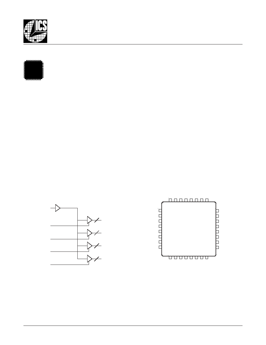
B
LOCK
D
IAGRAM
P
IN
A
SSIGNMENT
F
EATURES
� Sixteen 1.2V LVCMOS / LVTTL outputs
� LVCMOS / LVTTL clock input
� Maximum output frequency: 150MHz
� Output skew: TBD
� Propagation delay: 3.5ns (typical)
� 3.3V core/1.2V output operating supply mode
� 0�C to 70�C ambient operating temperature
� Industrial temperature information available upon request
� Available in both standard and lead-free RoHS-compliant
packages
HiPerClockSTM
ICS
32 31 30 29 28 27 26 25
9 10 11 12 13 14 15 16
1
2
3
4
5
6
7
8
24
23
22
21
20
19
18
17
V
DDO
QC0
QC1
QC2
QC3
GND
OEC
GND
V
DDO
QA0
QA1
QA2
QA3
GND
OEA
CLK
ICS8316
32-Lead VFQFN
5mm x 5mm x 0.95 package body
K Package
Top View
QA0:QA3
CLK
OEA
OEB
OEC
OED
V
DD
OEB
GND
QB3
QB2
QB1
QB0
V
DDO
GND
OED
GND
QD3
QD2
QD1
QD0
V
DDO
4
4
4
4
QB0:QB3
QC0:QC3
QD0:QD3
The Preliminary Information presented herein represents a product in prototyping or pre-production. The noted characteristics are based on
initial product characterization. Integrated Circuit Systems, Incorporated (ICS) reserves the right to change any circuitry or specifications
without notice.

8316AK
http://www.icst.com/products/hiperclocks.html
REV. A DECEMBER 22, 2005
2
Integrated
Circuit
Systems, Inc.
ICS8316
L
OW
S
KEW
, 1-
TO
-16, LVCMOS / LVTTL
F
ANOUT
B
UFFER
W
/1.2V LVCMOS O
UTPUTS
PRELIMINARY
T
ABLE
1. P
IN
D
ESCRIPTIONS
T
ABLE
2. P
IN
C
HARACTERISTICS
T
ABLE
3A. O
UTPUT
E
NABLE
AND
C
LOCK
E
NABLE
F
UNCTION
T
ABLE
T
ABLE
3B. C
LOCK
I
NPUT
F
UNCTION
T
ABLE
r
e
b
m
u
N
e
m
a
N
e
p
y
T
n
o
i
t
p
i
r
c
s
e
D
5
2
,
4
2
,
6
1
,
1
V
O
D
D
r
e
w
o
P
.
s
n
i
p
y
l
p
p
u
s
t
u
p
t
u
O
5
,
4
,
3
,
2
3
A
Q
,
2
A
Q
,
1
A
Q
,
0
A
Q
t
u
p
t
u
O
.
s
l
e
v
e
l
e
c
a
f
r
e
t
n
i
L
T
T
V
L
/
S
O
M
C
V
L
.
s
t
u
p
t
u
o
k
c
o
l
c
A
k
n
a
B
,
7
1
,
1
1
,
6
2
3
,
0
3
,
9
1
D
N
G
r
e
w
o
P
.
d
n
u
o
r
g
y
l
p
p
u
s
r
e
w
o
P
7
A
E
O
t
u
p
n
I
p
u
ll
u
P
g
n
il
b
a
s
i
d
d
n
a
g
n
il
b
a
n
e
s
l
o
r
t
n
o
C
.
n
i
p
e
l
b
a
n
e
t
u
p
t
u
o
A
k
n
a
B
.
s
l
e
v
e
l
e
c
a
f
r
e
t
n
i
L
T
T
V
L
/
S
O
M
C
V
L
.
s
t
u
p
t
u
o
3
A
Q
:
0
A
Q
f
o
8
K
L
C
t
u
p
n
I
n
w
o
d
ll
u
P
.
s
l
e
v
e
l
e
c
a
f
r
e
t
n
i
L
T
T
V
L
/
S
O
M
C
V
L
.
t
u
p
n
i
k
c
o
l
C
9
V
D
D
r
e
w
o
P
.
n
i
p
y
l
p
p
u
s
e
r
o
C
0
1
B
E
O
t
u
p
n
I
p
u
ll
u
P
g
n
il
b
a
s
i
d
d
n
a
g
n
il
b
a
n
e
s
l
o
r
t
n
o
C
.
n
i
p
e
l
b
a
n
e
t
u
p
t
u
o
B
k
n
a
B
.
s
l
e
v
e
l
e
c
a
f
r
e
t
n
i
L
T
T
V
L
/
S
O
M
C
V
L
.
s
t
u
p
t
u
o
3
B
Q
:
0
B
Q
f
o
5
1
,
4
1
,
3
1
,
2
1
0
B
Q
,
1
B
Q
,
2
B
Q
,
3
B
Q
t
u
p
t
u
O
.
s
l
e
v
e
l
e
c
a
f
r
e
t
n
i
L
T
T
V
L
/
S
O
M
C
V
L
.
s
t
u
p
t
u
o
k
c
o
l
c
B
k
n
a
B
8
1
C
E
O
t
u
p
n
I
p
u
ll
u
P
g
n
il
b
a
s
i
d
d
n
a
g
n
il
b
a
n
e
s
l
o
r
t
n
o
C
.
n
i
p
e
l
b
a
n
e
t
u
p
t
u
o
C
k
n
a
B
.
s
l
e
v
e
l
e
c
a
f
r
e
t
n
i
L
T
T
V
L
/
S
O
M
C
V
L
.
s
t
u
p
t
u
o
3
C
Q
:
0
C
Q
f
o
3
2
,
2
2
,
1
2
,
0
2
0
C
Q
,
1
C
Q
,
2
C
Q
,
3
C
Q
t
u
p
t
u
O
.
s
l
e
v
e
l
e
c
a
f
r
e
t
n
i
L
T
T
V
L
/
S
O
M
C
V
L
.
s
t
u
p
t
u
o
k
c
o
l
c
C
k
n
a
B
9
2
,
8
2
,
7
2
,
6
2
3
D
Q
,
2
D
Q
,
1
D
Q
,
0
D
Q
t
u
p
t
u
O
.
s
l
e
v
e
l
e
c
a
f
r
e
t
n
i
L
T
T
V
L
/
S
O
M
C
V
L
.
s
t
u
p
t
u
o
k
c
o
l
c
D
k
n
a
B
1
3
D
E
O
t
u
p
n
I
p
u
ll
u
P
g
n
il
b
a
s
i
d
d
n
a
g
n
il
b
a
n
e
s
l
o
r
t
n
o
C
.
n
i
p
e
l
b
a
n
e
t
u
p
t
u
o
D
k
n
a
B
.
s
l
e
v
e
l
e
c
a
f
r
e
t
n
i
L
T
T
V
L
/
S
O
M
C
V
L
.
s
t
u
p
t
u
o
3
D
Q
:
0
D
Q
f
o
:
E
T
O
N
p
u
ll
u
P
d
n
a
n
w
o
d
ll
u
P
.
s
e
u
l
a
v
l
a
c
i
p
y
t
r
o
f
,
s
c
i
t
s
i
r
e
t
c
a
r
a
h
C
n
i
P
,
2
e
l
b
a
T
e
e
S
.
s
r
o
t
s
i
s
e
r
t
u
p
n
i
l
a
n
r
e
t
n
i
o
t
r
e
f
e
r
s
t
u
p
n
I
s
t
u
p
t
u
O
]
D
:
A
[
E
O
K
L
C
3
x
Q
:
0
x
Q
1
0
W
O
L
1
1
H
G
I
H
l
o
b
m
y
S
r
e
t
e
m
a
r
a
P
s
n
o
i
t
i
d
n
o
C
t
s
e
T
m
u
m
i
n
i
M
l
a
c
i
p
y
T
m
u
m
i
x
a
M
s
t
i
n
U
C
N
I
e
c
n
a
t
i
c
a
p
a
C
t
u
p
n
I
4
F
p
C
D
P
e
c
n
a
t
i
c
a
p
a
C
n
o
i
t
a
p
i
s
s
i
D
r
e
w
o
P
)
t
u
p
t
u
o
r
e
p
(
V
O
D
D
V
6
2
.
1
=
D
B
T
F
p
R
P
U
L
L
U
P
r
o
t
s
i
s
e
R
p
u
ll
u
P
t
u
p
n
I
1
5
k
R
N
W
O
D
L
L
U
P
r
o
t
s
i
s
e
R
n
w
o
d
ll
u
P
t
u
p
n
I
1
5
k
R
T
U
O
e
c
n
a
d
e
p
m
I
t
u
p
t
u
O
V
O
D
D
%
5
�
2
.
1
=
5
1
s
t
u
p
n
I
l
o
r
t
n
o
C
s
t
u
p
t
u
O
]
D
:
A
[
E
O
3
x
Q
:
0
x
Q
0
Z
-
i
H
1
e
v
i
t
c
A
8316AK
http://www.icst.com/products/hiperclocks.html
REV. A DECEMBER 22, 2005
3
Integrated
Circuit
Systems, Inc.
ICS8316
L
OW
S
KEW
, 1-
TO
-16, LVCMOS / LVTTL
F
ANOUT
B
UFFER
W
/1.2V LVCMOS O
UTPUTS
PRELIMINARY
T
ABLE
4A. P
OWER
S
UPPLY
DC C
HARACTERISTICS
,
V
DD
= 3.3V, V
DDO
= 1.2V�5%, T
A
= 0�C
TO
70�C
l
o
b
m
y
S
r
e
t
e
m
a
r
a
P
s
n
o
i
t
i
d
n
o
C
t
s
e
T
m
u
m
i
n
i
M
l
a
c
i
p
y
T
m
u
m
i
x
a
M
s
t
i
n
U
V
D
D
e
g
a
t
l
o
V
y
l
p
p
u
S
e
r
o
C
5
3
1
.
3
3
.
3
5
6
4
.
3
V
V
O
D
D
e
g
a
t
l
o
V
y
l
p
p
u
S
t
u
p
t
u
O
4
1
.
1
2
.
1
6
2
.
1
V
I
D
D
t
n
e
r
r
u
C
y
l
p
p
u
S
r
e
w
o
P
D
B
T
A
�
I
O
D
D
t
n
e
r
r
u
C
y
l
p
p
u
S
t
u
p
t
u
O
D
B
T
A
�
A
BSOLUTE
M
AXIMUM
R
ATINGS
Supply Voltage, V
DD
4.6V
Inputs, V
I
-0.5V to V
DD
+ 0.5 V
Outputs, V
O
-0.5V to V
DDO
+ 0.5V
Package Thermal Impedance,
JA
34.8�C/W (0 lfpm)
Storage Temperature, T
STG
-65�C to 150�C
NOTE: Stresses beyond those listed under Absolute
Maximum Ratings may cause permanent damage to the
device. These ratings are stress specifications only. Functional
operation of product at these conditions or any conditions be-
yond those listed in the
DC Characteristics
or
AC Character-
istics
is not implied. Exposure to absolute maximum rating
conditions for extended periods may affect product reliability.
T
ABLE
4B. LVCMOS DC C
HARACTERISTICS
,
T
A
= 0�C
TO
70�C
l
o
b
m
y
S
r
e
t
e
m
a
r
a
P
s
n
o
i
t
i
d
n
o
C
t
s
e
T
m
u
m
i
n
i
M
l
a
c
i
p
y
T
m
u
m
i
x
a
M
s
t
i
n
U
V
H
I
e
g
a
t
l
o
V
h
g
i
H
t
u
p
n
I
2
V
D
D
3
.
0
+
V
V
L
I
e
g
a
t
l
o
V
w
o
L
t
u
p
n
I
3
.
0
-
8
.
0
V
I
H
I
t
n
e
r
r
u
C
h
g
i
H
t
u
p
n
I
K
L
C
V
D
D
V
=
N
I
V
5
6
4
.
3
=
0
5
1
A
�
D
E
O
:
A
E
O
V
D
D
V
=
N
I
V
5
6
4
.
3
=
5
A
�
I
L
I
t
n
e
r
r
u
C
w
o
L
t
u
p
n
I
K
L
C
V
D
D
V
,
V
5
6
4
.
3
=
N
I
V
0
=
5
-
A
�
D
E
O
:
A
E
O
V
D
D
V
,
V
5
6
4
.
3
=
N
I
V
0
=
0
5
1
-
A
�
V
H
O
e
g
a
t
l
o
V
h
g
i
H
t
u
p
t
u
O
V
O
D
D
1
E
T
O
N
;
%
5
�
V
2
.
1
=
V
D
D
7
.
0
*
V
V
L
O
e
g
a
t
l
o
V
w
o
L
t
u
p
t
u
O
V
O
D
D
1
E
T
O
N
;
%
5
�
V
2
.
1
=
V
D
D
3
.
0
*
V
0
5
h
t
i
w
d
e
t
a
n
i
m
r
e
t
s
t
u
p
t
u
O
:
1
E
T
O
N
V
o
t
O
D
D
.
m
a
r
g
a
i
d
"
t
i
u
c
r
i
C
t
s
e
T
d
a
o
L
"
,
n
o
i
t
c
e
s
t
n
e
m
e
r
u
s
a
e
M
r
e
t
e
m
a
r
a
P
e
e
S
.
2
/
T
ABLE
5. AC C
HARACTERISTICS
,
V
DD
= 3.3V�5%, V
DDO
= 1.2V�5%, T
A
= 0�C
TO
70�C
l
o
b
m
y
S
r
e
t
e
m
a
r
a
P
s
n
o
i
t
i
d
n
o
C
t
s
e
T
m
u
m
i
n
i
M
l
a
c
i
p
y
T
m
u
m
i
x
a
M
s
t
i
n
U
f
X
A
M
y
c
n
e
u
q
e
r
F
t
u
p
t
u
O
0
5
1
z
H
M
p
t
H
L
1
E
T
O
N
;
h
g
i
H
o
t
w
o
L
y
a
l
e
D
n
o
i
t
a
g
a
p
o
r
P
5
.
3
s
n
t
)
o
(
k
s
5
,
2
E
T
O
N
;
w
e
k
S
t
u
p
t
u
O
D
B
T
s
p
t
)
p
p
(
k
s
5
,
3
E
T
O
N
;
w
e
k
S
t
r
a
P
-
o
t
-
t
r
a
P
D
B
T
s
p
t
R
/t
F
4
E
T
O
N
;
e
m
i
T
e
s
i
R
t
u
p
t
u
O
%
0
8
o
t
%
0
2
0
5
6
s
p
c
d
o
e
l
c
y
C
y
t
u
D
t
u
p
t
u
O
0
5
%
f
t
a
d
e
r
u
s
a
e
m
s
r
e
t
e
m
a
r
a
p
ll
A
X
A
M
.
e
s
i
w
r
e
h
t
o
d
e
t
o
n
s
s
e
l
n
u
V
m
o
r
f
d
e
r
u
s
a
e
M
:
1
E
T
O
N
D
D
V
o
t
t
u
p
n
i
e
h
t
f
o
2
/
O
D
D
.
t
u
p
t
u
o
e
h
t
f
o
2
/
V
t
a
d
e
r
u
s
a
e
M
.
s
n
o
i
t
i
d
n
o
c
d
a
o
l
l
a
u
q
e
h
t
i
w
d
n
a
e
g
a
t
l
o
v
y
l
p
p
u
s
e
m
a
s
e
h
t
t
a
s
t
u
p
t
u
o
n
e
e
w
t
e
b
w
e
k
s
s
a
d
e
n
i
f
e
D
:
2
E
T
O
N
O
D
D
.
2
/
l
a
u
q
e
h
t
i
w
d
n
a
s
e
g
a
t
l
o
v
y
l
p
p
u
s
e
m
a
s
e
h
t
t
a
g
n
i
t
a
r
e
p
o
s
e
c
i
v
e
d
t
n
e
r
e
f
f
i
d
n
o
s
t
u
p
t
u
o
n
e
e
w
t
e
b
w
e
k
s
e
h
t
s
a
d
e
n
i
f
e
D
:
3
E
T
O
N
V
t
a
d
e
r
u
s
a
e
m
e
r
a
s
t
u
p
t
u
o
e
h
t
,
e
c
i
v
e
d
h
c
a
e
n
o
s
t
u
p
n
i
f
o
e
p
y
t
e
m
a
s
e
h
t
g
n
i
s
U
.
s
n
o
i
t
i
d
n
o
c
d
a
o
l
O
D
D
.
2
/
.
n
o
i
t
c
u
d
o
r
p
n
i
d
e
t
s
e
t
t
o
N
.
n
o
i
t
a
z
i
r
e
t
c
a
r
a
h
c
y
b
d
e
e
t
n
a
r
a
u
g
e
r
a
s
r
e
t
e
m
a
r
a
p
e
s
e
h
T
:
4
E
T
O
N
.
5
6
d
r
a
d
n
a
t
S
C
E
D
E
J
h
t
i
w
e
c
n
a
d
r
o
c
c
a
n
i
d
e
n
i
f
e
d
s
i
r
e
t
e
m
a
r
a
p
s
i
h
T
:
5
E
T
O
N
8316AK
http://www.icst.com/products/hiperclocks.html
REV. A DECEMBER 22, 2005
4
Integrated
Circuit
Systems, Inc.
ICS8316
L
OW
S
KEW
, 1-
TO
-16, LVCMOS / LVTTL
F
ANOUT
B
UFFER
W
/1.2V LVCMOS O
UTPUTS
PRELIMINARY
Clock
Outputs
20%
80%
80%
20%
t
R
t
F
t
PERIOD
t
PW
t
PERIOD
odc =
V
DDO
2
x 100%
t
PW
t
PD
V
DD
2
V
DDO
2
CLK
QA0:QA3,
QB0:QB3,
QC0:QC3,
QD0:QD3
O
UTPUT
R
ISE
/F
ALL
T
IME
QA0:QA3,
QB0:QB3,
QC0:QC3,
QD0:QD3
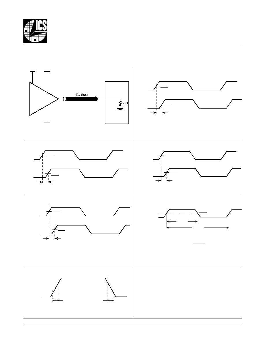
P
ARAMETER
M
EASUREMENT
I
NFORMATION
SCOPE
Qx
LVCMOS
2.7V�5%
V
DDO
-0.6V�5%
V
DD
0.6V�5%
P
ART
-
TO
-P
ART
S
KEW
GND
O
UTPUT
D
UTY
C
YCLE
/P
LUSE
W
IDTH
/P
ERIOD
P
ROPAGATION
D
ELAY
t
sk(o)
V
DDO
2
V
DDO
2
Qy
Qx
t
sk(pp)
V
DDO
2
V
DDO
2
Qy
Qx
Part 1
Part 2
B
ANK
S
KEW
(
where x denotes outputs in the same bank
)
t
sk(b)
V
DDO
2
V
DDO
2
Qx0:Qx3
Qx0:Qx3
O
UTPUT
S
KEW
3.3V C
ORE
/1.2V O
UTPUT
L
OAD
AC T
EST
C
IRCUIT

8316AK
http://www.icst.com/products/hiperclocks.html
REV. A DECEMBER 22, 2005
5
Integrated
Circuit
Systems, Inc.
ICS8316
L
OW
S
KEW
, 1-
TO
-16, LVCMOS / LVTTL
F
ANOUT
B
UFFER
W
/1.2V LVCMOS O
UTPUTS
PRELIMINARY
R
ELIABILITY
I
NFORMATION
T
RANSISTOR
C
OUNT
The transistor count for ICS8316 is: 416
T
ABLE
6.
JA
VS
. A
IR
F
LOW
T
ABLE
FOR
32 L
EAD
VFQFN
JA
vs. 0 Air Flow (Linear Feet per Minute)
0
Multi-Layer PCB, JEDEC Standard Test Boards
34.8�C/W
A
PPLICATION
I
NFORMATION
I
NPUTS
:
LVCMOS C
ONTROL
P
INS
:
All control pins have internal pull-ups or pull-downs; additional
resistance is not required but can be added for additional
protection. A 1k
resistor can be used.
R
ECOMMENDATIONS
FOR
U
NUSED
I
NPUT
AND
O
UTPUT
P
INS
O
UTPUTS
:
LVCMOS O
UTPUT
:
All unused LVCMOS output can be left floating. We
recommend that there is no trace attached.

8316AK
http://www.icst.com/products/hiperclocks.html
REV. A DECEMBER 22, 2005
6
Integrated
Circuit
Systems, Inc.
ICS8316
L
OW
S
KEW
, 1-
TO
-16, LVCMOS / LVTTL
F
ANOUT
B
UFFER
W
/1.2V LVCMOS O
UTPUTS
PRELIMINARY
T
ABLE
7. P
ACKAGE
D
IMENSIONS
P
ACKAGE
O
UTLINE
AND
D
IMENSIONS
- K S
UFFIX
FOR
32 L
EAD
VFQFN
Reference Document: JEDEC Publication 95, MO-220
N
O
I
T
A
I
R
A
V
C
E
D
E
J
S
R
E
T
E
M
I
L
L
I
M
N
I
S
N
O
I
S
N
E
M
I
D
L
L
A
L
O
B
M
Y
S
2
-
D
H
H
V
M
U
M
I
N
I
M
L
A
N
I
M
O
N
M
U
M
I
X
A
M
N
2
3
A
0
8
.
0
-
-
0
0
.
1
1
A
0
-
-
5
0
.
0
3
A
.
f
e
R
5
2
.
0
b
8
1
.
0
5
2
.
0
0
3
.
0
N
D
8
N
E
8
D
C
I
S
A
B
0
0
.
5
2
D
5
2
.
1
5
2
.
2
5
2
.
3
E
C
I
S
A
B
0
0
.
5
2
E
5
2
.
1
5
2
.
2
5
2
.
3
e
C
I
S
A
B
0
5
.
0
L
0
3
.
0
0
4
.
0
0
5
.
0
8316AK
http://www.icst.com/products/hiperclocks.html
REV. A DECEMBER 22, 2005
7
Integrated
Circuit
Systems, Inc.
ICS8316
L
OW
S
KEW
, 1-
TO
-16, LVCMOS / LVTTL
F
ANOUT
B
UFFER
W
/1.2V LVCMOS O
UTPUTS
PRELIMINARY
T
ABLE
8. O
RDERING
I
NFORMATION
While the information presented herein has been checked for both accuracy and reliability, Integrated Circuit Systems, Incorporated (ICS) assumes no responsibility for either its use
or for infringement of any patents or other rights of third parties, which would result from its use. No other circuits, patents, or licenses are implied. This product is intended for use
in normal commercial applications. Any other applications such as those requiring extended temperature range, high reliability, or other extraordinary environmental requirements are
not recommended without additional processing by ICS. ICS reserves the right to change any circuitry or specifications without notice. ICS does not authorize or warrant any ICS
product for use in life support devices or critical medical instruments.
The aforementioned trademark, HiPerClockSTM is a trademark of Integrated Circuit Systems, Inc. or its subsidiaries in the United States and/or other countries.
r
e
b
m
u
N
r
e
d
r
O
/
t
r
a
P
g
n
i
k
r
a
M
e
g
a
k
c
a
P
g
n
i
g
a
k
c
a
P
g
n
i
p
p
i
h
S
e
r
u
t
a
r
e
p
m
e
T
K
A
6
1
3
8
S
C
I
K
A
6
1
3
8
S
C
I
N
F
Q
F
V
d
a
e
L
2
3
y
a
r
t
C
�
0
7
o
t
C
�
0
T
K
A
6
1
3
8
S
C
I
K
A
6
1
3
8
S
C
I
N
F
Q
F
V
d
a
e
L
2
3
l
e
e
r
&
e
p
a
t
0
0
5
2
C
�
0
7
o
t
C
�
0
F
L
K
A
6
1
3
8
S
C
I
D
B
T
N
F
Q
F
V
"
e
e
r
F
-
d
a
e
L
"
d
a
e
L
2
3
y
a
r
t
C
�
0
7
o
t
C
�
0
T
F
L
K
A
6
1
3
8
S
C
I
D
B
T
N
F
Q
F
V
"
e
e
r
F
-
d
a
e
L
"
d
a
e
L
2
3
l
e
e
r
&
e
p
a
t
0
0
5
2
C
�
0
7
o
t
C
�
0
.
t
n
a
il
p
m
o
c
S
H
o
R
e
r
a
d
n
a
n
o
i
t
a
r
u
g
i
f
n
o
c
e
e
r
F
-
b
P
e
h
t
e
r
a
r
e
b
m
u
n
t
r
a
p
e
h
t
o
t
x
i
f
f
u
s
"
F
L
"
n
a
h
t
i
w
d
e
r
e
d
r
o
e
r
a
t
a
h
t
s
t
r
a
P
:
E
T
O
N