 | –≠–ª–µ–∫—Ç—Ä–æ–Ω–Ω—ã–π –∫–æ–º–ø–æ–Ω–µ–Ω—Ç: ICS8343 | –°–∫–∞—á–∞—Ç—å:  PDF PDF  ZIP ZIP |
Integrated
Circuit
Systems, Inc.
ICS8343
L
OW
S
KEW
1-
TO
-16
F
ANOUT
B
UFFER
8343
www.icst.com
REV. C, 07072000
1
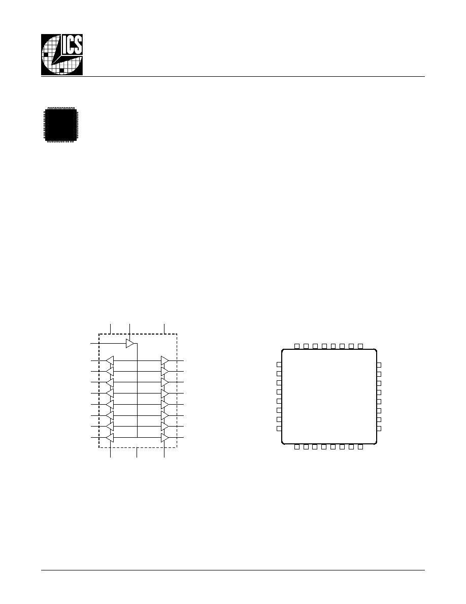
CLK
OE2
Q15
Q14
Q13
Q12
Q11
Q10
Q9
Q8
OE1
Q0
Q1
Q2
Q3
Q4
Q5
Q6
Q7
VDD1
VDD2
VDD
GND
G
ENERAL
D
ESCRIPTION
The ICS8343 is a low skew, 1-to-16 Fanout
Buffer and a member of the HiPerClockS
family of High Performance Clock Solutions
from ICS. The ICS8343 is at 3.3V, 2.5V and
mixed 3.3V input and 2.5V supply modes over
the commercial temperature range. Guaranteed output and
part-to-part skew characteristics make the ICS8343 ideal for
those clock distribution applications demanding well defined
performance and repeatability.
B
LOCK
D
IAGRAM
P
IN
A
SSIGNMENT
F
EATURES
∑
16 LVCMOS outputs
∑
Output frequency up to 200MHz
∑
250ps output skew
∑
700ps part to part
∑
CMOS compatible clock input at 5V, LVTTL and LVCMOS
compatible at 3.3V and 2.5V
∑
LVTTL output enable inputs
∑
Dual output enable inputs facilitates 1-to-16 or 1-to-8 input to
output modes
∑
3.3V, 2.5V or mixed 3.3V, 2.5V from 0∞C to 70∞C ambient
operating temperature
∑
32 lead low-profile QFP(LQFP), 7mm x 7mm x 1.4mm
package body, 0.8mm package lead pitch
HiPerClockSTM
,&6
32 31 30 29 28 27 26 25
9 10 11 12 13 14 15 16
1
2
3
4
5
6
7
8
24
23
22
21
20
19
18
17
VDD2
VDD2
VDD2
Q12
Q11
GND
GND
GND
VDD1
VDD1
VDD1
Q3
Q4
GND
GND
GND
Q10
Q9
Q8
VDD
CLK
Q7
Q6
Q5
Q13
Q14
Q15
OE2
OE1
Q0
Q1
Q2
ICS8343
32-Lead LQFP
(Top View)

8343
www.icst.com
REV. C, 07072000
2
Integrated
Circuit
Systems, Inc.
ICS8343
L
OW
S
KEW
1-
TO
-16
F
ANOUT
B
UFFER
T
ABLE
1. P
IN
D
ESCRIPTIONS
T
ABLE
2. P
IN
C
HARACTERISTICS
T
ABLE
3. F
UNCTION
T
ABLE
Inputs
Outputs
OE1
OE2
Q0 thru Q7
Q8 thru Q15
0
0
Hi Z
Hi Z
1
0
Active
Hi Z
0
1
Hi Z
Active
1
1
Active
Active
l
o
b
m
y
S
r
e
t
e
m
a
r
a
P
s
n
o
it
i
d
n
o
C
t
s
e
T
m
u
m
i
n
i
M
l
a
c
i
p
y
T
m
u
m
i
x
a
M
s
ti
n
U
N
I
C
e
c
n
a
ti
c
a
p
a
C
t
u
p
n
I
F
p
D
P
C
e
c
n
a
ti
c
a
p
a
C
n
o
it
a
p
i
s
s
i
D
r
e
w
o
P
)t
u
p
t
u
o
r
e
p
(
V
5
2
.
5
=
2
D
D
V
,
1
D
D
V
5
1
F
p
V
7
4
.
3
=
2
D
D
V
,
1
D
D
V
1
1
F
p
V
3
6
.
2
=
2
D
D
V
,
1
D
D
V
5
.
9
F
p
r
e
b
m
u
N
e
m
a
N
e
p
y
T
n
o
it
p
i
r
c
s
e
D
3
,
2
,
1
1
D
D
V
r
e
w
o
P
.
V
5
.
2
r
o
V
3
.
3
,
V
5
o
t
t
c
e
n
n
o
C
.
y
l
p
p
u
s
r
e
w
o
p
7
Q
u
r
h
t
0
Q
t
u
p
t
u
O
5
,
4
4
Q
,
3
Q
t
u
p
t
u
O
4
1
.
s
t
u
p
t
u
o
k
c
o
l
C
.
e
c
n
a
d
e
p
m
i
t
u
p
t
u
o
l
a
c
i
p
y
t
8
,
7
,
6
D
N
G
r
e
w
o
P
.
d
n
u
o
r
g
o
t
t
c
e
n
n
o
C
1
1
,
0
1
,
9
7
Q
,
6
Q
,
5
Q
t
u
p
t
u
O
4
1
.
s
t
u
p
t
u
o
k
c
o
l
C
.
e
c
n
a
d
e
p
m
i
t
u
p
t
u
o
l
a
c
i
p
y
t
2
1
K
L
C
t
u
p
n
I
.t
u
p
n
i
k
c
o
l
C
3
1
D
D
V
r
e
w
o
P
V
5
.
2
r
o
V
3
.
3
,
V
5
o
t
t
c
e
n
n
o
C
.
y
l
p
p
u
s
r
e
w
o
p
t
u
p
n
I
6
1
,
5
1
,
4
1
0
1
Q
,
9
Q
,
8
Q
t
u
p
t
u
O
4
1
.
s
t
u
p
t
u
o
k
c
o
l
C
.
e
c
n
a
d
e
p
m
i
t
u
p
t
u
o
l
a
c
i
p
y
t
9
1
,
8
1
,
7
1
D
N
G
r
e
w
o
P
.
d
n
u
o
r
g
o
t
t
c
e
n
n
o
C
1
2
,
0
2
2
1
Q
,
1
1
Q
t
u
p
t
u
O
4
1
.
s
t
u
p
t
u
o
k
c
o
l
C
.
e
c
n
a
d
e
p
m
i
t
u
p
t
u
o
l
a
c
i
p
y
t
4
2
,
3
2
,
2
2
2
D
D
V
r
e
w
o
P
.
V
5
.
2
r
o
V
3
.
3
,
V
5
o
t
t
c
e
n
n
o
C
.
y
l
p
p
u
s
r
e
w
o
p
5
1
Q
u
r
h
t
8
Q
t
u
p
t
u
O
7
2
,
6
2
,
5
2
5
1
Q
,
4
1
Q
,
3
1
Q
t
u
p
t
u
O
4
1
.
s
t
u
p
t
u
o
k
c
o
l
C
.
e
c
n
a
d
e
p
m
i
t
u
p
t
u
o
l
a
c
i
p
y
t
8
2
2
E
O
t
u
p
n
I
p
u
ll
u
P
.
e
t
a
t
s
Z
i
H
o
t
5
1
Q
u
r
h
t
8
Q
s
t
u
p
t
u
o
s
e
c
r
o
f
w
o
l
n
e
h
W
.
e
l
b
a
n
e
t
u
p
t
u
O
9
2
1
E
O
t
u
p
n
I
p
u
ll
u
P
.
e
t
a
t
s
Z
i
H
o
t
7
Q
u
r
h
t
0
Q
s
t
u
p
t
u
o
s
e
c
r
o
f
w
o
l
n
e
h
W
.
e
l
b
a
n
e
t
u
p
t
u
O
2
3
,
1
3
,
0
3
2
Q
,
1
Q
,
0
Q
t
u
p
t
u
O
4
1
.
s
t
u
p
t
u
o
k
c
o
l
C
.
e
c
n
a
d
e
p
m
i
t
u
p
t
u
o
l
a
c
i
p
y
t
Integrated
Circuit
Systems, Inc.
ICS8343
L
OW
S
KEW
1-
TO
-16
F
ANOUT
B
UFFER
8343
www.icst.com
REV. C, 07072000
3
T
ABLE
5A. AC E
LECTRICAL
C
HARACTERISTICS
,
VDD = VDD1 = VDD2 = 3.3V±5%, T
A
= 0∞
TO
70∞C
T
ABLE
4A. DC E
LECTRICAL
C
HARACTERISTICS
,
VDD = VDD1 = VDD2 = 3.3V±5%, T
A
= 0∞
TO
70∞C
l
o
b
m
y
S
r
e
t
e
m
a
r
a
P
s
n
o
it
i
d
n
o
C
t
s
e
T
m
u
m
i
n
i
M
l
a
c
i
p
y
T
m
u
m
i
x
a
M
s
ti
n
U
2
D
D
V
,
1
D
D
V
,
D
D
V
e
g
a
tl
o
V
y
l
p
p
u
S
g
n
it
a
r
e
p
O
5
3
1
.
3
3
.
3
5
6
4
.
3
V
H
I
V
e
g
a
tl
o
V
h
g
i
H
t
u
p
n
I
K
L
C
V
5
6
4
.
3
=
D
D
V
2
3
.
0
+
D
D
V
V
x
E
O
V
5
6
4
.
3
=
D
D
V
2
3
.
0
+
D
D
V
V
L
I
V
e
g
a
tl
o
V
w
o
L
t
u
p
n
I
K
L
C
V
5
3
1
.
3
=
D
D
V
3
.
0
-
8
.
0
V
x
E
O
V
5
3
1
.
3
=
D
D
V
3
.
0
-
8
.
0
V
H
II
t
n
e
r
r
u
C
h
g
i
H
t
u
p
n
I
K
L
C
D
D
V
=
N
I
V
1
A
µ
x
E
O
D
D
V
=
N
I
V
1
A
µ
L
II
t
n
e
r
r
u
C
w
o
L
t
u
p
n
I
K
L
C
V
0
=
N
I
V
5
1
-
A
µ
x
E
O
V
0
=
N
I
V
5
1
-
A
µ
D
D
I
t
n
e
r
r
u
C
y
l
p
p
u
S
g
n
it
a
r
e
p
O
t
u
p
n
I
0
0
1
A
µ
H
O
V
e
g
a
tl
o
V
h
g
i
H
t
u
p
t
u
O
A
m
5
2
-
=
H
O
I
,
V
5
3
1
.
3
=
D
D
V
4
.
2
V
L
O
V
e
g
a
tl
o
V
w
o
L
t
u
p
t
u
O
A
m
5
2
=
L
O
I
,
V
5
3
1
.
3
=
D
D
V
8
.
0
V
H
Z
O
I
t
n
e
r
r
u
C
e
g
a
k
a
e
L
e
c
n
a
d
e
p
m
I
h
g
i
H
D
D
V
=
T
U
O
V
,
V
0
=
x
E
O
1
A
µ
L
Z
O
I
t
n
e
r
r
u
C
e
g
a
k
a
e
L
e
c
n
a
d
e
p
m
I
h
g
i
H
=
T
U
O
V
,
V
0
=
x
E
O
V
0
1
-
A
µ
l
o
b
m
y
S
r
e
t
e
m
a
r
a
P
s
n
o
it
i
d
n
o
C
t
s
e
T
m
u
m
i
n
i
M
l
a
c
i
p
y
T
m
u
m
i
x
a
M
s
ti
n
U
X
A
M
f
y
c
n
e
u
q
e
r
F
t
u
p
n
I
m
u
m
i
x
a
M
0
0
2
z
H
M
H
L
p
t
h
g
i
H
-
o
t-
w
o
L
,
y
a
l
e
D
n
o
it
a
g
a
p
o
r
P
0
<
f
z
H
M
0
0
2
1
.
1
1
.
2
1
.
3
s
n
L
H
p
t
w
o
L
-
o
t-
h
g
i
H
,
y
a
l
e
D
n
o
it
a
g
a
p
o
r
P
0
<
f
z
H
M
0
0
2
2
.
1
0
.
2
7
.
2
s
n
)
o
(
k
s
t
3
E
T
O
N
;
w
e
k
S
t
u
p
t
u
O
2
/
x
D
D
V
@
e
g
d
e
g
n
i
s
ir
n
o
d
e
r
u
s
a
e
M
0
5
2
s
p
)
p
(
k
s
t
4
E
T
O
N
;
w
e
k
S
s
s
e
c
o
r
P
2
/
x
D
D
V
@
e
g
d
e
g
n
i
s
ir
n
o
d
e
r
u
s
a
e
M
0
5
4
s
p
)
p
p
(
k
s
t
5
E
T
O
N
;
w
e
k
S
tr
a
P
-
o
t-
tr
a
P
2
/
x
D
D
V
@
e
g
d
e
g
n
i
s
ir
n
o
d
e
r
u
s
a
e
M
0
0
7
s
p
R
t
e
m
i
T
e
s
i
R
t
u
p
t
u
O
5
.
0
8
.
0
s
n
F
t
e
m
i
T
ll
a
F
t
u
p
t
u
O
9
.
0
7
.
1
s
n
W
P
t
h
t
d
i
W
e
s
l
u
P
t
u
p
t
u
O
2
/
E
L
C
Y
C
t
5
.
0
-
2
/
E
L
C
Y
C
t
2
/
E
L
C
Y
C
t
5
.
0
+
s
n
.
e
s
i
w
r
e
h
t
o
d
e
t
o
n
s
s
e
l
n
u
X
A
M
f
t
a
d
e
r
u
s
a
e
m
s
r
e
t
e
m
a
r
a
p
ll
A
:
1
E
T
O
N
0
5
h
ti
w
d
e
t
a
n
i
m
r
e
t
s
t
u
p
t
u
O
:
2
E
T
O
N
.
2
/
x
D
D
V
o
t
d
e
t
c
e
n
n
o
c
r
o
t
s
i
s
e
r
.
s
n
o
it
i
d
n
o
c
d
a
o
l
l
a
u
q
e
h
ti
w
d
n
a
s
e
g
a
tl
o
v
y
l
p
p
u
s
e
m
a
s
e
h
t
t
a
s
t
u
p
t
u
o
s
s
o
r
c
a
w
e
k
s
s
a
d
e
n
if
e
D
:
3
E
T
O
N
.
s
n
o
it
i
d
n
o
c
d
a
o
l
l
a
u
q
e
h
ti
w
d
n
a
s
e
g
a
tl
o
v
y
l
p
p
u
s
e
m
a
s
e
h
t
t
a
g
n
it
a
r
e
p
o
s
e
c
i
v
e
d
t
n
e
r
e
ff
i
d
n
o
t
u
p
t
u
o
e
m
a
s
e
h
t
t
a
w
e
k
s
s
a
d
e
n
if
e
D
:
4
E
T
O
N
.
s
n
o
it
i
d
n
o
c
d
a
o
l
l
a
u
q
e
h
ti
w
d
n
a
s
e
g
a
tl
o
v
y
l
p
p
u
s
e
m
a
s
e
h
t
t
a
g
n
it
a
r
e
p
o
s
e
c
i
v
e
d
t
n
e
r
e
ff
i
d
n
o
s
t
u
p
t
u
o
t
n
e
r
e
ff
i
d
t
a
w
e
k
s
s
a
d
e
n
if
e
D
:
5
E
T
O
N
A
BSOLUTE
M
AXIMUM
R
ATINGS
Supply Voltage
7V
Inputs
-0.5V to VDD+0.5 V
Outputs
-0.5V to VDD+0.5V
Ambient Operating Temperature
0∞C to 70∞C
Storage Temperature
-65∞C to 150∞C
Stresses beyond those listed under Absolute Maximum Ratings may cause permanent damage to the device. These ratings are stress specifi-
cations only and functional operation of the device at these or any conditions beyond those listed in the DC Electrical Characteristics or AC Electrical
Characteristics is not implied. Exposure to absolute maximum rating conditions for extended periods may affect product reliability.

8343
www.icst.com
REV. C, 07072000
4
Integrated
Circuit
Systems, Inc.
ICS8343
L
OW
S
KEW
1-
TO
-16
F
ANOUT
B
UFFER
T
ABLE
5B. AC E
LECTRICAL
C
HARACTERISTICS
,
VDD = 3.3V±5%, VDD1 = VDD2 = 2.5V±5%, T
A
= 0∞
TO
70∞C
T
ABLE
4B. DC E
LECTRICAL
C
HARACTERISTICS
,
VDD = 3.3V±5%, VDD1 = VDD2 = 2.5V±5%, T
A
= 0∞
TO
70∞C
l
o
b
m
y
S
r
e
t
e
m
a
r
a
P
s
n
o
it
i
d
n
o
C
t
s
e
T
m
u
m
i
n
i
M
l
a
c
i
p
y
T
m
u
m
i
x
a
M
s
ti
n
U
D
D
V
e
g
a
tl
o
V
y
l
p
p
u
S
g
n
it
a
r
e
p
O
t
u
p
n
I
5
3
1
.
3
3
.
3
5
6
4
.
3
V
2
D
D
V
,
1
D
D
V
e
g
a
tl
o
V
y
l
p
p
u
S
g
n
it
a
r
e
p
O
t
u
p
t
u
O
5
7
3
.
2
5
.
2
5
2
6
.
2
H
I
V
e
g
a
tl
o
V
h
g
i
H
t
u
p
n
I
K
L
C
5
6
4
.
3
=
D
D
V
2
3
.
0
+
D
D
V
V
x
E
O
5
6
4
.
3
=
D
D
V
2
3
.
0
+
D
D
V
V
L
I
V
e
g
a
tl
o
V
w
o
L
t
u
p
n
I
K
L
C
5
3
1
.
3
=
D
D
V
3
.
0
-
8
.
0
V
x
E
O
5
3
1
.
3
=
D
D
V
3
.
0
-
8
.
0
V
H
II
t
n
e
r
r
u
C
h
g
i
H
t
u
p
n
I
K
L
C
D
D
V
=
N
I
V
1
A
µ
x
E
O
D
D
V
=
N
I
V
1
A
µ
L
II
t
n
e
r
r
u
C
w
o
L
t
u
p
n
I
K
L
C
V
0
=
N
I
V
5
1
-
A
µ
x
E
O
V
0
=
N
I
V
5
1
-
A
µ
D
D
I
t
n
e
r
r
u
C
y
l
p
p
u
S
g
n
it
a
r
e
p
O
t
u
p
n
I
0
0
1
A
µ
H
O
V
e
g
a
tl
o
V
h
g
i
H
t
u
p
t
u
O
A
m
5
2
-
=
H
O
I
,
V
5
7
3
.
2
=
D
D
V
5
.
1
V
L
O
V
e
g
a
tl
o
V
w
o
L
t
u
p
t
u
O
A
m
5
2
=
L
O
I
,
V
5
7
3
.
2
=
D
D
V
8
.
0
V
H
Z
O
I
t
n
e
r
r
u
C
e
g
a
k
a
e
L
e
c
n
a
d
e
p
m
I
h
g
i
H
D
D
V
=
T
U
O
V
,
V
0
=
x
E
O
1
A
µ
L
Z
O
I
t
n
e
r
r
u
C
e
g
a
k
a
e
L
e
c
n
a
d
e
p
m
I
h
g
i
H
=
T
U
O
V
,
V
0
=
x
E
O
V
0
1
-
A
µ
l
o
b
m
y
S
r
e
t
e
m
a
r
a
P
s
n
o
it
i
d
n
o
C
t
s
e
T
m
u
m
i
n
i
M
l
a
c
i
p
y
T
m
u
m
i
x
a
M
s
ti
n
U
X
A
M
f
y
c
n
e
u
q
e
r
F
t
u
p
n
I
m
u
m
i
x
a
M
0
0
2
z
H
M
H
L
p
t
h
g
i
H
-
o
t-
w
o
L
,
y
a
l
e
D
n
o
it
a
g
a
p
o
r
P
0
<
f
z
H
M
0
0
2
0
.
1
3
.
2
2
.
3
s
n
L
H
p
t
w
o
L
-
o
t-
h
g
i
H
,
y
a
l
e
D
n
o
it
a
g
a
p
o
r
P
0
<
f
z
H
M
0
0
2
4
.
1
3
.
2
2
.
3
s
n
)
o
(
k
s
t
3
E
T
O
N
;
w
e
k
S
t
u
p
t
u
O
2
/
x
D
D
V
@
e
g
d
e
g
n
i
s
ir
n
o
d
e
r
u
s
a
e
M
0
5
2
s
p
)
p
(
k
s
t
4
E
T
O
N
;
w
e
k
S
s
s
e
c
o
r
P
2
/
x
D
D
V
@
e
g
d
e
g
n
i
s
ir
n
o
d
e
r
u
s
a
e
M
0
5
4
s
p
)
p
p
(
k
s
t
5
E
T
O
N
;
w
e
k
S
tr
a
P
-
o
t-
tr
a
P
2
/
x
D
D
V
@
e
g
d
e
g
n
i
s
ir
n
o
d
e
r
u
s
a
e
M
0
0
7
s
p
R
t
e
m
i
T
e
s
i
R
t
u
p
t
u
O
5
.
0
8
.
0
s
n
F
t
e
m
i
T
ll
a
F
t
u
p
t
u
O
9
.
0
7
.
1
s
n
W
P
t
h
t
d
i
W
e
s
l
u
P
t
u
p
t
u
O
2
/
E
L
C
Y
C
t
5
.
0
-
2
/
E
L
C
Y
C
t
2
/
E
L
C
Y
C
t
5
.
0
+
s
n
.
e
s
i
w
r
e
h
t
o
d
e
t
o
n
s
s
e
l
n
u
X
A
M
f
t
a
d
e
r
u
s
a
e
m
s
r
e
t
e
m
a
r
a
p
ll
A
:
1
E
T
O
N
0
5
h
ti
w
d
e
t
a
n
i
m
r
e
t
s
t
u
p
t
u
O
:
2
E
T
O
N
.
2
/
x
D
D
V
o
t
d
e
t
c
e
n
n
o
c
r
o
t
s
i
s
e
r
.
s
n
o
it
i
d
n
o
c
d
a
o
l
l
a
u
q
e
h
ti
w
d
n
a
s
e
g
a
tl
o
v
y
l
p
p
u
s
e
m
a
s
e
h
t
t
a
s
t
u
p
t
u
o
s
s
o
r
c
a
w
e
k
s
s
a
d
e
n
if
e
D
:
3
E
T
O
N
.
s
n
o
it
i
d
n
o
c
d
a
o
l
l
a
u
q
e
h
ti
w
d
n
a
s
e
g
a
tl
o
v
y
l
p
p
u
s
e
m
a
s
e
h
t
t
a
g
n
it
a
r
e
p
o
s
e
c
i
v
e
d
t
n
e
r
e
ff
i
d
n
o
t
u
p
t
u
o
e
m
a
s
e
h
t
t
a
w
e
k
s
s
a
d
e
n
if
e
D
:
4
E
T
O
N
.
s
n
o
it
i
d
n
o
c
d
a
o
l
l
a
u
q
e
h
ti
w
d
n
a
s
e
g
a
tl
o
v
y
l
p
p
u
s
e
m
a
s
e
h
t
t
a
g
n
it
a
r
e
p
o
s
e
c
i
v
e
d
t
n
e
r
e
ff
i
d
n
o
s
t
u
p
t
u
o
t
n
e
r
e
ff
i
d
t
a
w
e
k
s
s
a
d
e
n
if
e
D
:
5
E
T
O
N

Integrated
Circuit
Systems, Inc.
ICS8343
L
OW
S
KEW
1-
TO
-16
F
ANOUT
B
UFFER
8343
www.icst.com
REV. C, 07072000
5
T
ABLE
5C. AC E
LECTRICAL
C
HARACTERISTICS
,
VDD = VDD1 = VDD2 = 2.5V±5%, T
A
= 0∞
TO
70∞C
T
ABLE
4C. DC E
LECTRICAL
C
HARACTERISTICS
,
VDD = VDD1 = VDD2 = 2.5V±5%, T
A
= 0∞
TO
70∞C
l
o
b
m
y
S
r
e
t
e
m
a
r
a
P
s
n
o
it
i
d
n
o
C
t
s
e
T
m
u
m
i
n
i
M
l
a
c
i
p
y
T
m
u
m
i
x
a
M
s
ti
n
U
2
D
D
V
,
1
D
D
V
,
D
D
V
e
g
a
tl
o
V
y
l
p
p
u
S
g
n
it
a
r
e
p
O
5
7
3
.
2
5
.
2
5
2
6
.
2
V
H
I
V
e
g
a
tl
o
V
h
g
i
H
t
u
p
n
I
K
L
C
5
2
6
.
2
=
D
D
V
2
3
.
0
+
D
D
V
V
x
E
O
5
2
6
.
2
=
D
D
V
2
3
.
0
+
D
D
V
V
L
I
V
e
g
a
tl
o
V
w
o
L
t
u
p
n
I
K
L
C
5
7
3
.
2
=
D
D
V
3
.
0
-
7
.
0
V
x
E
O
5
7
3
.
2
=
D
D
V
3
.
0
-
8
.
0
V
H
II
t
n
e
r
r
u
C
h
g
i
H
t
u
p
n
I
K
L
C
D
D
V
=
N
I
V
1
A
µ
x
E
O
D
D
V
=
N
I
V
1
A
µ
L
II
t
n
e
r
r
u
C
w
o
L
t
u
p
n
I
K
L
C
V
0
=
N
I
V
0
1
-
A
µ
x
E
O
V
0
=
N
I
V
0
1
-
A
µ
D
D
I
t
n
e
r
r
u
C
y
l
p
p
u
S
g
n
it
a
r
e
p
O
t
u
p
n
I
0
0
1
A
µ
H
O
V
e
g
a
tl
o
V
h
g
i
H
t
u
p
t
u
O
A
m
5
2
-
=
H
O
I
,
V
5
7
3
.
2
=
D
D
V
5
.
1
V
L
O
V
e
g
a
tl
o
V
w
o
L
t
u
p
t
u
O
A
m
5
2
=
L
O
I
,
V
5
7
3
.
2
=
D
D
V
8
.
0
V
H
Z
O
I
t
n
e
r
r
u
C
e
g
a
k
a
e
L
e
c
n
a
d
e
p
m
I
h
g
i
H
D
D
V
=
T
U
O
V
,
V
0
=
x
E
O
1
A
µ
L
Z
O
I
t
n
e
r
r
u
C
e
g
a
k
a
e
L
e
c
n
a
d
e
p
m
I
h
g
i
H
V
0
=
T
U
O
V
,
V
0
=
x
E
O
1
-
A
µ
l
o
b
m
y
S
r
e
t
e
m
a
r
a
P
s
n
o
it
i
d
n
o
C
t
s
e
T
m
u
m
i
n
i
M
l
a
c
i
p
y
T
m
u
m
i
x
a
M
s
ti
n
U
X
A
M
f
y
c
n
e
u
q
e
r
F
t
u
p
n
I
m
u
m
i
x
a
M
3
3
1
z
H
M
H
L
p
t
h
g
i
H
-
o
t-
w
o
L
,
y
a
l
e
D
n
o
it
a
g
a
p
o
r
P
0
<
f
z
H
M
0
0
2
0
.
1
5
.
2
7
.
3
s
n
L
H
p
t
w
o
L
-
o
t-
h
g
i
H
,
y
a
l
e
D
n
o
it
a
g
a
p
o
r
P
0
<
f
z
H
M
0
0
2
4
.
1
6
.
2
5
.
3
s
n
)
o
(
k
s
t
3
E
T
O
N
;
w
e
k
S
t
u
p
t
u
O
2
/
x
D
D
V
@
e
g
d
e
g
n
i
s
ir
n
o
d
e
r
u
s
a
e
M
0
5
2
s
p
)
p
(
k
s
t
4
E
T
O
N
;
w
e
k
S
s
s
e
c
o
r
P
2
/
x
D
D
V
@
e
g
d
e
g
n
i
s
ir
n
o
d
e
r
u
s
a
e
M
0
0
5
s
p
)
p
p
(
k
s
t
5
E
T
O
N
;
w
e
k
S
tr
a
P
-
o
t-
tr
a
P
2
/
x
D
D
V
@
e
g
d
e
g
n
i
s
ir
n
o
d
e
r
u
s
a
e
M
0
5
7
s
p
R
t
e
m
i
T
e
s
i
R
t
u
p
t
u
O
5
.
0
8
.
0
s
n
F
t
e
m
i
T
ll
a
F
t
u
p
t
u
O
9
.
0
7
.
1
s
n
W
P
t
h
t
d
i
W
e
s
l
u
P
t
u
p
t
u
O
2
/
E
L
C
Y
C
t
5
7
.
0
-
2
/
E
L
C
Y
C
t
2
/
E
L
C
Y
C
t
5
7
.
0
+
s
n
.
e
s
i
w
r
e
h
t
o
d
e
t
o
n
s
s
e
l
n
u
X
A
M
f
t
a
d
e
r
u
s
a
e
m
s
r
e
t
e
m
a
r
a
p
ll
A
:
1
E
T
O
N
0
5
h
ti
w
d
e
t
a
n
i
m
r
e
t
s
t
u
p
t
u
O
:
2
E
T
O
N
.
2
/
x
D
D
V
o
t
d
e
t
c
e
n
n
o
c
r
o
t
s
i
s
e
r
.
s
n
o
it
i
d
n
o
c
d
a
o
l
l
a
u
q
e
h
ti
w
d
n
a
s
e
g
a
tl
o
v
y
l
p
p
u
s
e
m
a
s
e
h
t
t
a
s
t
u
p
t
u
o
s
s
o
r
c
a
w
e
k
s
s
a
d
e
n
if
e
D
:
3
E
T
O
N
.
s
n
o
it
i
d
n
o
c
d
a
o
l
l
a
u
q
e
h
ti
w
d
n
a
s
e
g
a
tl
o
v
y
l
p
p
u
s
e
m
a
s
e
h
t
t
a
g
n
it
a
r
e
p
o
s
e
c
i
v
e
d
t
n
e
r
e
ff
i
d
n
o
t
u
p
t
u
o
e
m
a
s
e
h
t
t
a
w
e
k
s
s
a
d
e
n
if
e
D
:
4
E
T
O
N
.
s
n
o
it
i
d
n
o
c
d
a
o
l
l
a
u
q
e
h
ti
w
d
n
a
s
e
g
a
tl
o
v
y
l
p
p
u
s
e
m
a
s
e
h
t
t
a
g
n
it
a
r
e
p
o
s
e
c
i
v
e
d
t
n
e
r
e
ff
i
d
n
o
s
t
u
p
t
u
o
t
n
e
r
e
ff
i
d
t
a
w
e
k
s
s
a
d
e
n
if
e
D
:
5
E
T
O
N
8343
www.icst.com
REV. C, 07072000
6
Integrated
Circuit
Systems, Inc.
ICS8343
L
OW
S
KEW
1-
TO
-16
F
ANOUT
B
UFFER
-A, B, OR -D-
e / 2
-A, B, OR -D-
b
-A, B, OR -D-
e / 2
-A, B, OR -D-
b
D
D/2
E
E/2
D1
D1/2
E1
E1/2
-A-
e
-D-
-B-
SEE DETA IL "A"
0.20 C A-B D
4X
NOTE 3
NOTE 3
NOTE 3
NOTE 4
N
O
T
E
4
N
O
T
E
5,
7
NOTE 5, 7
N/4 TIPS
D
D/2
E
E/2
D1
D1/2
E1
E1/2
-A-
e
-D-
-B-
SEE DETA IL "A"
0.20 C A-B D
4X
0.20 C A-B D
0.20 C A-B D
4X
NOTE 3
NOTE 3
NOTE 3
NOTE 4
N
O
T
E
4
N
O
T
E
5,
7
NOTE 5, 7
N/4 TIPS
0.25
0∞ MIN.
0∞ - 7 ∞
0.08
R. MIN.
0.20 MIN.
L
0.08/0.20 R.
GAUGE PLANE
1.00 REF.
-H-
A2
A1
DATUM
PLANE
- 0.05 S
0.25
0∞ MIN.
0∞ - 7 ∞
0.08
R. MIN.
0.20 MIN.
L
0.08/0.20 R.
GAUGE PLANE
1.00 REF.
-H-
A2
A1
DATUM
PLANE
- 0.05 S
- 0.05 S
ddd M C A-B S D S
b
b
1
0.09 / 0.20
0.09 / 0.16
BASE MET AL
WITH LEAD FINISH
SEE DETA IL "B"
ccc
8 PLACES
11 / 13∞
-C-
-H-
A
NOTE 2 / / 0.10 C
NOTE 9
ddd M C A-B S D S
b
b
1
0.09 / 0.20
0.09 / 0.16
BASE MET AL
WITH LEAD FINISH
SEE DETA IL "B"
ccc
8 PLACES
11 / 13∞
-C-
-H-
A
NOTE 2 / / 0.10 C
NOTE 9
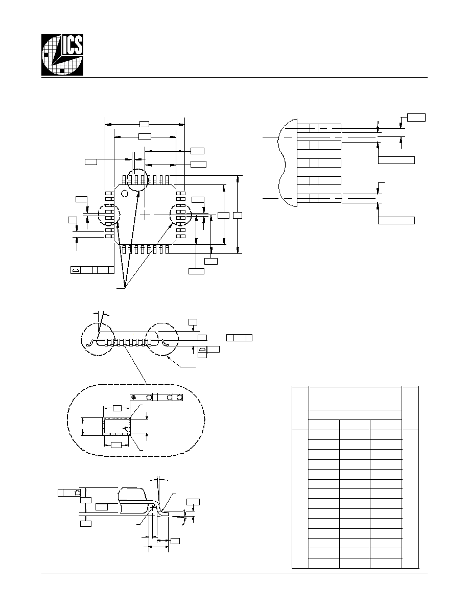
P
ACKAGE
O
UTLINE
& D
IMENSIONS
NOTES:
1. ALL DIMENSIONS AND TOLERANCING CONFORM TO
ANSI Y14.5-1982
2. DATUM PLANE -H- LOCATED AT MOLD PARTING
LINE AND COINCIDENT WITH LEAD, WHERE LEAD
EXITS PLASTIC BODY AT BOTTOM OF PARTING LINE.
3. DATUMS A-B AND -D- TO BE DETERMINED AT
CENTERLINE BETWEEN LEADS WHERE LEADS EXIT
PLASTIC AT DATUM PLANE -H- .
4. TO BE DETERMINED AT SEATING PLACE -C- .
5. DIMENSIONS D1 AND E1 DO NOT INCLUDE MOLD
PROTRUSION.
6. N IS THE TOTAL NUMBER OF TERMINALS.
7. THESE DIMENSIONS TO BE DETEREMINED AT DATUM
PLANE -H-.
8. PACKAGE TOP DIMENSIONS ARE SMALLER THAN
BOTTOM DIMENSIONS AND TOP OF PACKAGE WILL
NOT OVERHANG BOTTOM OF PACKAGE.
9. DIMENSION b DOES NOT INCLUDE DAMBAR
PROTRUSION. ALLOWABLE DAMBAR PROTRUSION
SHALL BE 0.08mm TOTAL IN EXCESS OF THE b
DIMENSION AT MAXIMUM MATERIAL CONDITION.
10. CONTROLLING DIMENSION: MILLIMETER.
11. THIS OUTLINE CONFORMS TO JEDEC PUBLIBCATION
95 REGISTRATION MS-026, VARIATION BBA.
12. A1 IS DEFINED AS THE DISTANCE FROM THE
SEATING PLANE TO THE LOWEST POINT OF THE
PACKAGE.
S
Y
M
B
O
L
N
O
I
T
A
I
R
A
V
C
E
D
E
J
S
R
E
T
E
M
I
L
L
I
M
N
I
S
N
O
I
S
N
E
M
I
D
L
L
A
N
O
T
E
A
B
B
N
I
M
M
O
N
X
A
M
A
0
6
.
1
1
A
5
0
.
0
5
1
.
0
2
1
2
A
5
3
.
1
4
.
1
5
4
.
1
D
.
C
S
B
0
0
.
9
4
1
D
.
C
S
B
0
0
.
7
8
,
7
E
.
C
S
B
0
0
.
9
4
1
E
.
C
S
B
0
0
.
7
8
,
7
L
5
4
.
0
0
6
.
0
5
7
.
0
N
2
3
e
.
C
S
B
0
8
.
0
b
0
3
.
0
7
3
.
0
5
4
.
0
1
b
0
3
.
0
5
3
.
0
0
4
.
0
9
c
c
c
0
1
.
0
d
d
d
0
2
.
0

Integrated
Circuit
Systems, Inc.
ICS8343
L
OW
S
KEW
1-
TO
-16
F
ANOUT
B
UFFER
8343
www.icst.com
REV. C, 07072000
7
O
RDERING
I
NFORMATION
While the information presented herein has been checked for both accuracy and reliability, Integrated Circuit Systems, Incorporated (ICS) assumes no responsibility for either its use or
for infringement of any patents or other rights of third parties, which would result from its use. No other circuits, patents, or licenses are implied. This product is intended for use in normal
commercial applications. Any other applications such as those requiring extended temperature range, high reliability, or other extraordinary environmental requirements are not recom-
mended without additional processing by ICS. ICS reserves the right to change any circuitry or specifications without notice. ICS does not authorize or warrant any ICS product for use
in life support devices or critical medical instruments.
r
e
b
m
u
N
r
e
d
r
O
/t
r
a
P
g
n
i
k
r
a
M
e
g
a
k
c
a
P
t
n
u
o
C
e
r
u
t
a
r
e
p
m
e
T
Y
3
4
3
8
S
C
I
Y
3
4
3
8
S
C
I
P
F
Q
L
d
a
e
L
2
3
y
a
rt
r
e
p
0
5
2
C
∞
0
7
o
t
C
∞
0
T
Y
3
4
3
8
S
C
I
Y
3
4
3
8
S
C
I
l
e
e
R
d
n
a
e
p
a
T
n
o
P
F
Q
L
d
a
e
L
2
3
0
0
0
2
C
∞
0
7
o
t
C
∞
0