Document Outline
- General Description
- Features
- Simplified Schematic
- Logic Diagram
- Pin Assignment
- Pin Descriptions
- Pin Characteristics
- Function Table
- Absolute Maximum Ratings
- Power Supply DC Characeristics
- DC Characeristics
- AC Characeristics
- Parameter Measurement Information
- Reliability Information
- Transistor Count
- Package Outline
- Package Dimensions
- Ordering Information
- Revision History Sheet

83841BH
www.icst.com/products/hiperclocks.html
REV. A JANUARY 20, 2006
1
Integrated
Circuit
Systems, Inc.
ICS83841
20 B
IT
, DDR SDRAM 2:1 MUX
G
ENERAL
D
ESCRIPTION
The ICS83841 is a 20 Bit, DDR SDRAM 2:1 MUX
and is a member of the HiPerClockSTM family of
High Performance Clock Solutions from ICS. The
device has 20 host lines and each host line can
be passed to 2 data ports. The host/data ports
are compatible with single-ended SSTL-2 and the device op-
erates from a 2.5V supply.
Guaranteed low output skew makes the ICS83841 ideal for
demanding applications which require well defined performance
and repeatability.
L
OGIC
D
IAGRAM
F
EATURES
� Forty low skew single-ended DIMM ports
� One SSTL-2 compatible select input
� Maximum Switching Speed: 3ns
� Output skew: 180ps (maximum)
� r
on
= 20
(typical)
� Full 2.5V supply modes
� 0�C to 70�C ambient operating temperature
� Available in both standard and lead-free RoHS compliant
packages
HiPerClockSTM
ICS
S
IMPLIFIED
S
CHEMATIC
DHx
S
DAx or DBx
R
PD
SW
DH0
DA0
DB0
DH19
Sw
Sw
DA19
DB19
Sw
Sw
S
r
on
r
on
ICS83841
72-Ball TFBGA
6mm x 6mm x 1.2mm
package body
H Package
Top View
P
IN
A
SSIGNMENT
B
D
7
1
A
D
7
1
B
D
6
1
B
D
5
1
A
D
5
1
B
D
4
1
A
D
4
1
A
D
3
1
B
D
2
1
A
D
2
1
A
D
8
1
H
D
7
1
H
D
6
1
A
D
6
1
H
D
5
1
H
D
4
1
B
D
3
1
H
D
3
1
H
D
2
1
B
D
1
1
B
D
8
1
H
D
8
1
D
N
G
D
N
G
H
D
1
1
A
D
1
1
A
D
9
1
D
N
G
D
N
G
B
D
0
1
B
D
9
1
H
D
9
1
S
V
D
D
H
D
0
1
A
D
0
1
A
D
0
H
D
0
V
D
D
V
D
D
H
D
9
B
D
9
B
D
0
D
N
G
D
N
G
A
D
9
A
D
1
H
D
1
D
N
G
D
N
G
H
D
8
B
D
8
B
D
1
H
D
2
H
D
3
B
D
3
H
D
4
H
D
5
A
D
6
H
D
6
H
D
7
A
D
8
A
D
2
B
D
2
A
D
3
A
D
4
B
D
4
A
D
5
B
D
5
B
D
6
A
D
7
B
D
7
1
2
3
4
5
6
7
8
9
10
A
B
C
D
E
F
G
H
J
K

83841BH
www.icst.com/products/hiperclocks.html
REV. A JANUARY 20, 2006
2
Integrated
Circuit
Systems, Inc.
ICS83841
20 B
IT
, DDR SDRAM 2:1 MUX
T
ABLE
1. P
IN
D
ESCRIPTIONS
r
e
b
m
u
N
e
m
a
N
e
p
y
T
n
o
i
t
p
i
r
c
s
e
D
8
F
,
3
F
,
8
E
V
D
D
r
e
w
o
P
.
s
n
i
p
y
l
p
p
u
s
e
v
i
t
i
s
o
P
6
H
,
5
H
,
9
G
,
2
G
,
9
D
,
2
D
,
6
C
,
5
C
D
N
G
r
e
w
o
P
.
d
n
u
o
r
g
y
l
p
p
u
s
r
e
w
o
P
3
E
S
t
u
p
n
I
t
s
o
H
s
t
c
e
l
e
S
.
t
u
p
n
I
l
o
r
t
n
o
C
.
3
e
l
b
a
T
r
e
p
n
o
i
t
c
n
u
f
t
r
o
P
,
9
B
,
8
B
,
6
B
,
5
B
,
3
B
,
2
B
,
2
H
,
9
F
,
2
F
,
9
E
,
2
E
,
9
C
2
C
9
J
,
8
J
,
6
J
,
5
J
,
3
J
,
2
J
,
9
H
,
2
1
H
D
,
3
1
H
D
,
4
1
H
D
,
5
1
H
D
,
6
1
H
D
,
7
1
H
D
,
1
H
D
,
9
H
D
,
0
H
D
,
0
1
H
D
,
9
1
H
D
,
1
1
H
D
,
8
1
H
D
7
H
D
,
6
H
D
,
5
H
D
,
4
H
D
,
3
H
D
,
2
H
D
,
8
H
D
t
r
o
P
.
s
t
r
o
p
t
s
o
H
,
1
B
,
0
1
A
,
8
A
,
7
A
,
5
A
,
2
A
,
1
H
,
0
1
G
,
1
F
,
0
1
E
,
1
D
,
0
1
C
,
4
B
9
K
,
6
K
,
4
K
,
3
K
,
1
K
,
0
1
J
,
7
J
,
8
1
A
D
,
2
1
A
D
,
3
1
A
D
,
4
1
A
D
,
5
1
A
D
,
7
1
A
D
,
1
A
D
,
9
A
D
,
0
A
D
,
0
1
A
D
,
9
1
A
D
,
1
1
A
D
,
6
1
A
D
7
A
D
,
5
A
D
,
4
A
D
,
3
A
D
,
2
A
D
,
8
A
D
,
6
A
D
t
r
o
P
.
s
t
r
o
p
M
M
I
D
,
7
B
,
9
A
,
6
A
,
4
A
,
3
A
,
1
A
,
0
1
H
,
1
G
,
0
1
F
,
1
E
,
0
1
D
,
1
C
,
0
1
B
0
1
K
,
8
K
,
7
K
,
5
K
,
2
K
,
4
J
,
1
J
,
3
1
B
D
,
2
1
B
D
,
4
1
B
D
,
5
1
B
D
,
6
1
B
D
,
7
1
B
D
,
8
B
D
,
0
B
D
,
9
B
D
,
9
1
B
D
,
0
1
B
D
,
8
1
B
D
,
1
1
B
D
7
B
D
,
6
B
D
,
5
B
D
,
4
B
D
,
2
B
D
,
3
B
D
,
1
B
D
t
r
o
P
.
s
t
r
o
p
M
M
I
D
T
ABLE
2. P
IN
C
HARACTERISTICS
T
ABLE
3. F
UNCTION
T
ABLE
t
u
p
n
I
l
o
r
t
n
o
C
n
o
i
t
c
n
u
F
S
L
s
t
r
o
P
M
M
I
D
B
=
t
r
o
P
t
s
o
H
0
4
1
=
t
r
o
P
M
M
I
D
A
D
N
G
o
t
H
s
t
r
o
P
M
M
I
D
A
=
t
r
o
P
t
s
o
H
0
4
1
=
t
r
o
P
M
M
I
D
B
D
N
G
o
t
l
o
b
m
y
S
r
e
t
e
m
a
r
a
P
s
n
o
i
t
i
d
n
o
C
t
s
e
T
m
u
m
i
n
i
M
l
a
c
i
p
y
T
m
u
m
i
x
a
M
s
t
i
n
U
C
N
I
e
c
n
a
t
i
c
a
p
a
C
n
i
P
l
o
r
t
n
o
C
V
I
V
r
o
V
0
=
D
D
5
F
p
C
N
O
e
c
n
a
t
i
c
a
p
a
C
n
o
l
e
n
n
a
h
C
V
N
I
V
5
.
1
=
0
1
F
p
83841BH
www.icst.com/products/hiperclocks.html
REV. A JANUARY 20, 2006
3
Integrated
Circuit
Systems, Inc.
ICS83841
20 B
IT
, DDR SDRAM 2:1 MUX
T
ABLE
4A. P
OWER
S
UPPLY
DC C
HARACTERISTICS
,
V
DD
= 2.5V � 0.2V, T
A
= 0�C
TO
70�C
l
o
b
m
y
S
r
e
t
e
m
a
r
a
P
s
n
o
i
t
i
d
n
o
C
t
s
e
T
m
u
m
i
n
i
M
l
a
c
i
p
y
T
m
u
m
i
x
a
M
s
t
i
n
U
V
D
D
e
g
a
t
l
o
V
y
l
p
p
u
S
e
v
i
t
i
s
o
P
3
.
2
5
.
2
7
.
2
V
I
D
D
t
n
e
r
r
u
C
y
l
p
p
u
S
r
e
w
o
P
0
2
A
�
T
ABLE
4B. DC C
HARACTERISTICS
,
V
DD
= 2.5V � 0.2V, T
A
= 0�C
TO
70�C
l
o
b
m
y
S
r
e
t
e
m
a
r
a
P
s
n
o
i
t
i
d
n
o
C
t
s
e
T
m
u
m
i
n
i
M
l
a
c
i
p
y
T
m
u
m
i
x
a
M
s
t
i
n
U
V
H
I
e
g
a
t
l
o
V
h
g
i
H
t
u
p
n
I
S
6
.
1
V
V
L
I
e
g
a
t
l
o
V
w
o
L
t
u
p
n
I
S
9
.
0
V
V
K
I
e
g
a
t
l
o
V
p
m
a
l
C
t
u
p
n
I
V
D
D
;
V
3
.
2
=
I
I
A
m
8
1
-
=
2
.
1
-
V
I
L
e
g
a
k
a
e
L
t
u
p
n
I
t
n
e
r
r
u
C
S
V
D
D
;
V
5
.
2
=
V
I
V
=
D
D
;
D
N
G
r
o
V
=
S
D
D
0
0
1
�
A
�
t
r
o
P
t
s
o
H
0
0
1
�
A
�
t
r
o
P
M
M
I
D
I
r
o
f
D
N
G
=
S
)
t
s
e
t
(
L
I
0
0
1
�
A
�
r
N
O
1
E
T
O
N
;
e
c
n
a
t
s
i
s
e
R
n
O
V
D
D
V
;
V
5
.
2
=
A
V
;
V
8
.
0
=
B
V
0
.
1
=
6
1
0
2
0
3
V
D
D
V
;
V
5
.
2
=
A
V
;
V
7
.
1
=
B
V
5
.
1
=
6
1
0
2
0
3
e
d
i
s
h
c
a
e
n
o
s
e
g
a
t
l
o
v
d
e
t
a
c
i
d
n
i
e
h
t
t
a
s
l
a
n
i
m
r
e
t
M
M
I
D
e
h
t
d
n
a
t
s
o
H
e
h
t
n
e
e
w
t
e
b
t
n
e
r
r
u
c
e
h
t
y
b
d
e
r
u
s
a
e
M
:
1
E
T
O
N
.
h
c
t
i
w
s
e
h
t
f
o
A
BSOLUTE
M
AXIMUM
R
ATINGS
Supply Voltage, V
DD
-0.5V to +3.3V
Inputs, V
I
-0.3V to V
DD
+ 0.3 V
Ports
DC Input Clamp Current, I
IK
-50mA
Package Thermal Impedance,
JA
50.04�C/W (0 mps)
Storage Temperature, T
STG
-65�C to 150�C
NOTE: Stresses beyond those listed under Absolute
Maximum Ratings may cause permanent damage to the
device. These ratings are stress specifications only. Functional
operation of product at these conditions or any conditions be-
yond those listed in the
DC Characteristics
or
AC Character-
istics
is not implied. Exposure to absolute maximum rating
conditions for extended periods may affect product reliability.
T
ABLE
5. AC C
HARACTERISTICS
,
V
DD
= 2.5V � 0.2V, T
A
= 0�C
TO
70�C
l
o
b
m
y
S
r
e
t
e
m
a
r
a
P
s
n
o
i
t
i
d
n
o
C
t
s
e
T
m
u
m
i
n
i
M
l
a
c
i
p
y
T
m
u
m
i
x
a
M
s
t
i
n
U
t
D
P
;
y
a
l
e
D
n
o
i
t
a
g
a
p
o
r
P
3
,
1
E
T
O
N
x
B
D
/
x
A
D
r
o
x
H
D
m
o
r
F
x
H
D
r
o
x
B
D
/
x
A
D
o
t
5
2
1
0
4
2
s
p
t
N
E
t
u
p
t
u
O
e
m
i
T
e
l
b
a
n
E
o
t
S
m
o
r
F
x
B
D
/
x
A
D
r
o
x
H
D
2
.
1
s
n
t
S
I
D
t
u
p
t
u
O
e
m
i
T
e
l
b
a
s
i
D
o
t
S
m
o
r
F
x
B
D
/
x
A
D
r
o
x
H
D
2
.
1
s
n
t
K
S
O
;
w
e
k
S
t
u
p
t
u
O
3
,
2
E
T
O
N
t
r
o
P
y
n
a
o
t
t
r
o
P
y
n
A
0
8
1
s
p
V
m
o
r
f
d
e
r
u
s
a
e
M
:
1
E
T
O
N
D
D
o
t
t
u
p
n
i
e
h
t
f
o
2
/
V
D
D
.
t
u
p
t
u
o
e
h
t
f
o
2
/
V
t
a
d
e
r
u
s
a
e
M
.
s
n
o
i
t
i
d
n
o
c
d
a
o
l
l
a
u
q
e
h
t
i
w
d
n
a
e
g
a
t
l
o
v
y
l
p
p
u
s
e
m
a
s
e
h
t
t
a
s
t
u
p
t
u
o
n
e
e
w
t
e
b
w
e
k
s
s
a
d
e
n
i
f
e
D
:
2
E
T
O
N
D
D
.
2
/
.
n
o
i
t
a
z
i
r
e
t
c
a
r
a
h
c
y
b
d
e
e
t
n
a
r
a
u
g
,
d
e
t
s
e
t
n
o
i
t
c
u
d
o
r
p
t
o
N
:
3
E
T
O
N
83841BH
www.icst.com/products/hiperclocks.html
REV. A JANUARY 20, 2006
4
Integrated
Circuit
Systems, Inc.
ICS83841
20 B
IT
, DDR SDRAM 2:1 MUX
t
PD
V
DD
2
V
DD
2
P
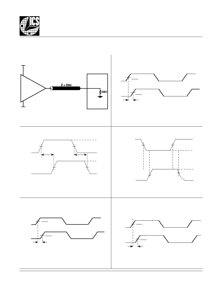
ARAMETER
M
EASUREMENT
I
NFORMATION
O
UTPUT
S
KEW
2.5V O
UTPUT
L
OAD
AC T
EST
C
IRCUIT
B
ANK
S
KEW
t
sk(o)
V
DD
2
V
DD
2
DAx,
DBx
DAy,
DBy
DHx
DAx/DBx
1.25V
1.25V
1.25V
2.5V
0V
V
OH
V
OL
Input
Output
Rising Edge
Skew
FallingEdge
Skew
1.25V
1.25V
1.25V
1.25V
V
OH
- 0.15V
V
OL
V
OH
0V
2.5V
t
PHZ
t
PZH
Output DAx/DBx
(See Note)
S
(Low-level
enabling)
NOTE: The output is high except when disabled by the S control.
3-S
TATE
O
UTPUT
E
NABLE
/D
ISABLE
T
IMES
R
ISING
& F
ALLING
E
DGE
S
KEW
P
ROPAGATION
D
ELAY
t
sk(b)
V
DD
2
V
DD
2
DAx
DBx
V
DD
= 1.25V � 0.1V
-1.25V � 0.1V
SCOPE
Qx
LVCMOS
V
DD
GND
This circuit is used for test purposes only,
not intended for application use.

83841BH
www.icst.com/products/hiperclocks.html
REV. A JANUARY 20, 2006
5
Integrated
Circuit
Systems, Inc.
ICS83841
20 B
IT
, DDR SDRAM 2:1 MUX
R
ELIABILITY
I
NFORMATION
T
RANSISTOR
C
OUNT
The transistor count for ICS83841 is: 261
T
ABLE
6.
JA
VS
. A
IR
F
LOW
T
ABLE
FOR
A
72-B
ALL
TFBGA
JA
by Velocity (Millimeter Feet per Second)
0
1
2
Two-Layer PCB, JEDEC Standard Test Boards
50.04�C/W
43.18�C/W
41.17�C/W
NOTE: Most modern PCB designs use multi-layered boards. The data in the second row pertains to most designs.

83841BH
www.icst.com/products/hiperclocks.html
REV. A JANUARY 20, 2006
6
Integrated
Circuit
Systems, Inc.
ICS83841
20 B
IT
, DDR SDRAM 2:1 MUX
P
ACKAGE
O
UTLINE
- H S
UFFIX
FOR
A
72-B
ALL
TFBGA
T
ABLE
7. P
ACKAGE
D
IMENSIONS
R
EFERENCE
D
OCUMENT
: JEDEC P
UBLICATION
95, MO-195
N
O
I
T
A
I
R
A
V
C
E
D
E
J
S
R
E
T
E
M
I
L
L
I
M
N
I
S
N
O
I
S
N
E
M
I
D
L
L
A
L
O
B
M
Y
S
A
G
B
F
M
U
M
I
N
I
M
L
A
N
I
M
O
N
M
U
M
I
X
A
M
n
r
e
t
t
a
P
0
1
x
0
1
,
m
m
6
x
6
,
s
ll
a
B
2
7
A
0
.
1
1
.
1
2
.
1
1
A
5
6
1
.
0
2
.
0
5
3
2
.
0
b
5
2
.
0
3
.
0
5
3
.
0
D
C
S
B
0
0
.
6
1
D
C
S
B
0
5
.
4
E
C
S
B
0
0
.
6
1
E
C
S
B
0
5
.
4
e
C
S
B
0
5
.
0

83841BH
www.icst.com/products/hiperclocks.html
REV. A JANUARY 20, 2006
7
Integrated
Circuit
Systems, Inc.
ICS83841
20 B
IT
, DDR SDRAM 2:1 MUX
T
ABLE
8. O
RDERING
I
NFORMATION
While the information presented herein has been checked for both accuracy and reliability, Integrated Circuit Systems, Incorporated (ICS) assumes no responsibility for either its use
or for infringement of any patents or other rights of third parties, which would result from its use. No other circuits, patents, or licenses are implied. This product is intended for use
in normal commercial applications. Any other applications such as those requiring extended temperature range, high reliability, or other extraordinary environmental requirements
are not recommended without additional processing by ICS. ICS reserves the right to change any circuitry or specifications without notice. ICS does not authorize or warrant any ICS
product for use in life support devices or critical medical instruments.
The aforementioned trademark, HiPerClockS is a trademark of Integrated Circuit Systems, Inc. or its subsidiaries in the United States and/or other countries.
r
e
b
m
u
N
r
e
d
r
O
/
t
r
a
P
g
n
i
k
r
a
M
e
g
a
k
c
a
P
g
n
i
g
a
k
c
a
P
g
n
i
p
p
i
h
S
e
r
u
t
a
r
e
p
m
e
T
H
B
1
4
8
3
8
S
C
I
H
B
1
4
8
3
8
S
C
I
A
G
B
F
T
ll
a
B
-
2
7
D
B
T
C
�
0
7
o
t
C
�
0
T
H
B
1
4
8
3
8
S
C
I
H
B
1
4
8
3
8
S
C
I
A
G
B
F
T
ll
a
B
-
2
7
l
e
e
R
&
e
p
a
T
0
0
5
2
C
�
0
7
o
t
C
�
0
F
L
H
B
1
4
8
3
8
S
C
I
F
L
H
B
1
4
8
3
8
S
C
I
A
G
B
F
T
,
e
e
r
F
d
a
e
L
,
ll
a
B
-
2
7
D
B
T
C
�
0
7
o
t
C
�
0
T
F
L
H
B
1
4
8
3
8
S
C
I
F
L
H
B
1
4
8
3
8
S
C
I
A
G
B
F
T
,
e
e
r
F
d
a
e
L
,
ll
a
B
-
2
7
l
e
e
R
&
e
p
a
T
0
0
5
2
C
�
0
7
o
t
C
�
0
.
t
n
a
il
p
m
o
c
S
H
o
R
e
r
a
d
n
a
n
o
i
t
a
r
u
g
i
f
n
o
c
e
e
r
F
-
b
P
e
h
t
e
r
a
r
e
b
m
u
n
t
r
a
p
e
h
t
o
t
x
i
f
f
u
s
"
F
L
"
n
a
h
t
i
w
d
e
r
e
d
r
o
e
r
a
t
a
h
t
s
t
r
a
P
:
E
T
O
N

83841BH
www.icst.com/products/hiperclocks.html
REV. A JANUARY 20, 2006
8
Integrated
Circuit
Systems, Inc.
ICS83841
20 B
IT
, DDR SDRAM 2:1 MUX
T
E
E
H
S
Y
R
O
T
S
I
H
N
O
I
S
I
V
E
R
v
e
R
e
l
b
a
T
e
g
a
P
e
g
n
a
h
C
f
o
n
o
i
t
p
i
r
c
s
e
D
e
t
a
D
A
8
T
8
d
e
d
d
a
d
n
a
g
n
i
k
r
a
m
e
e
r
F
-
d
a
e
L
d
e
t
c
e
r
r
o
c
-
e
l
b
a
t
n
o
i
t
a
m
r
o
f
n
I
g
n
i
r
e
d
r
O
.
e
t
o
n
e
e
r
F
-
d
a
e
L
6
0
/
0
2
/
1