Document Outline
- General Description
- Features
- Block Diagram
- Pin Assignment
- Pin Descriptions
- Pin Characteristics
- Output Enable & Clock Enable Function Table
- Absolute Maximum Ratings
- Power Supply DC Characteristics
- LVCMOS 3.3V DC Characteristics
- LVCMOS 2.5V DC Characteristics
- 3.3V AC Characteristics
- 2.5V AC Characteristics
- Additive Phase Jitter
- Parameter Measurement Information
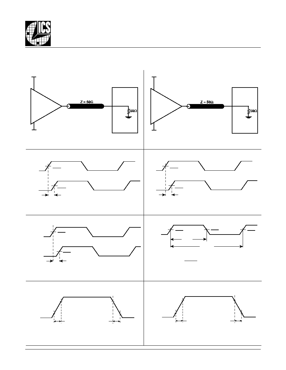
- 3.3V Output Load AC Test Circuit Diagram
- 2.5V Output Load AC Test Circulit Diagram
- Part-to-Part Skew Diagram
- Output Skew Diagram
- Propagation delay Diagram
- Ouput Duty Cycle/Pulse Width/Period Diagram
- 3.3V Output Rise/Fall Time Diagram
- 2.5V Output Rise/Fall Time Diagram
- Application Schematic Example
- Reliability Information
- Transistor Count
- Package Outline
- Package Dimensions
- Ordering Information
83947AYI-147
http://www.icst.com/products/hiperclocks.html
REV. A SEPTEMBER 24, 2004
1
Integrated
Circuit
Systems, Inc.
ICS83947I-147
L
OW
S
KEW
, 1-
TO
-9
LVCMOS/LVTTL F
ANOUT
B
UFFER
G
ENERAL
D
ESCRIPTION
The ICS83947I-147 is a low skew, 1-to-9
LVCMOS/LVTTL Fanout Buffer and a member of
the HiPerClockSTM family of High Performance
Clock Solutions from ICS. The low impedance
LVCMOS/LVTTL outputs are designed to drive 50
series or parallel terminated transmission lines. The effective
fanout can be increased from 9 to 18 by utilizing the ability of
the outputs to drive two series terminated lines.
Guaranteed output and part-to-part skew characteristics make
the ICS83947I-147 ideal for high performance, 3.3V or 2.5V
single ended applications.
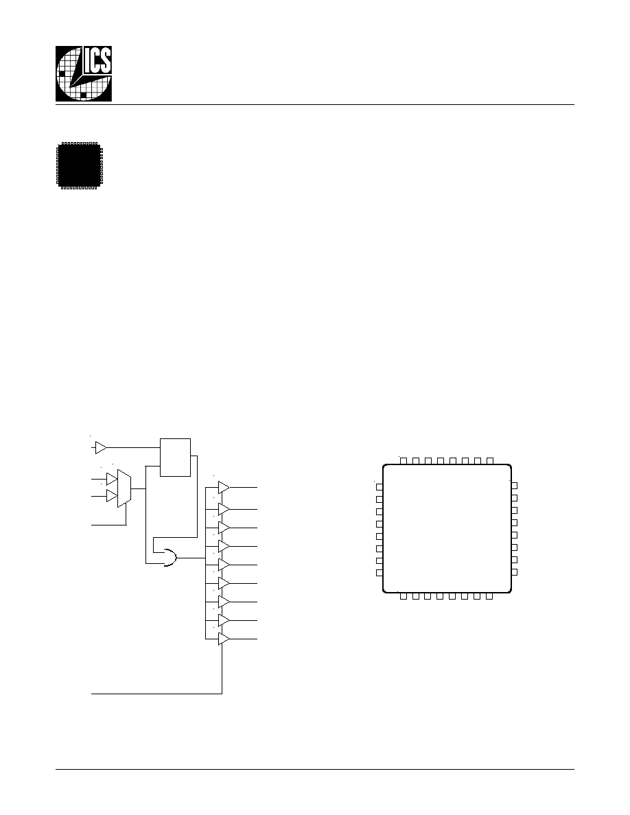
B
LOCK
D
IAGRAM
P
IN
A
SSIGNMENT
F
EATURES
∑ 9 LVCMOS/LVTTL outputs
∑ Selectable CLK0 and CLK1 can accept the following
input levels: LVCMOS and LVTTL
∑ Maximum output frequency: 250MHz
∑ Output skew: 115ps (maximum)
∑ Part-to-part skew: 500ps (maximum)
∑ Additive phase jitter, RMS: 0.02ps (typical) @ 3.3V
∑ Full 3.3V or 2.5V operating supply
∑ -40∞C to 85∞C ambient operating temperature
∑ Pin compatible with the MPC947
HiPerClockSTM
ICS
32-Lead LQFP
7mm x 7mm x 1.4mm package body
Y Package
Top View
32 31 30 29 28 27 26 25
9 10 11 12 13 14 15 16
1
2
3
4
5
6
7
8
24
23
22
21
20
19
18
17
GND
Q3
V
DDO
Q4
GND
Q5
V
DDO
GND
GND
CLK_SEL
CLK0
CLK1
CLK_EN
OE
V
DD
GND
GND
Q6
V
DDO
Q7
GND
Q8
V
DDO
GND
GND
Q2
V
DDO
Q1
GND
Q0
V
DDO
GND
ICS83947I-147
Q0
Q1
Q2
Q3
Q4
Q5
Q6
Q7
Q8
CLK0
CLK1
0
1
CLK_EN
CLK_SEL
D
Q
LE
OE
83947AYI-147
http://www.icst.com/products/hiperclocks.html
REV. A SEPTEMBER 24, 2004
2
Integrated
Circuit
Systems, Inc.
ICS83947I-147
L
OW
S
KEW
, 1-
TO
-9
LVCMOS/LVTTL F
ANOUT
B
UFFER
T
ABLE
1. P
IN
D
ESCRIPTIONS
T
ABLE
2. P
IN
C
HARACTERISTICS
T
ABLE
3. O
UTPUT
E
NABLE
AND
C
LOCK
E
NABLE
F
UNCTION
T
ABLE
r
e
b
m
u
N
e
m
a
N
e
p
y
T
n
o
i
t
p
i
r
c
s
e
D
,
7
1
,
6
1
,
2
1
,
9
,
8
,
1
2
3
,
9
2
,
5
2
,
4
2
,
0
2
D
N
G
r
e
w
o
P
.
d
n
u
o
r
g
y
l
p
p
u
s
r
e
w
o
P
2
L
E
S
_
K
L
C
t
u
p
n
I
p
u
ll
u
P
,
W
O
L
n
e
h
W
.
1
K
L
C
s
t
c
e
l
e
s
,
H
G
I
H
n
e
h
W
.
t
u
p
n
i
t
c
e
l
e
s
k
c
o
l
C
.
s
l
e
v
e
l
e
c
a
f
r
e
t
n
i
L
T
T
V
L
/
S
O
M
C
V
L
.
0
K
L
C
s
t
c
e
l
e
s
4
,
3
1
K
L
C
,
0
K
L
C
t
u
p
n
I
p
u
ll
u
P
.
s
l
e
v
e
l
e
c
a
f
r
e
t
n
i
L
T
T
V
L
/
S
O
M
C
V
L
.
s
t
u
p
n
i
k
c
o
l
c
e
c
n
e
r
e
f
e
R
5
N
E
_
K
L
C
t
u
p
n
I
p
u
ll
u
P
.
s
l
e
v
e
l
e
c
a
f
r
e
t
n
i
L
T
T
V
L
/
S
O
M
C
V
L
.
e
l
b
a
n
e
k
c
o
l
C
6
E
O
t
u
p
n
I
p
u
ll
u
P
.
s
l
e
v
e
l
e
c
a
f
r
e
t
n
i
L
T
T
V
L
/
S
O
M
C
V
L
.
e
l
b
a
n
e
t
u
p
t
u
O
7
V
D
D
r
e
w
o
P
.
n
i
p
y
l
p
p
u
s
e
r
o
C
1
3
,
7
2
,
2
2
,
8
1
,
4
1
,
0
1
V
O
D
D
r
e
w
o
P
.
s
n
i
p
y
l
p
p
u
s
t
u
p
t
u
O
,
1
2
,
9
1
,
5
1
,
3
1
,
1
1
0
3
,
8
2
,
6
2
,
3
2
,
5
Q
,
6
Q
,
7
Q
,
8
Q
0
Q
,
1
Q
,
2
Q
,
3
Q
,
4
Q
t
u
p
t
u
O
.
s
t
u
p
t
u
o
k
c
o
l
c
8
Q
u
r
h
t
0
Q
.
s
l
e
v
e
l
e
c
a
f
r
e
t
n
i
L
T
T
V
L
/
S
O
M
C
V
L
:
E
T
O
N
p
u
ll
u
P
.
s
e
u
l
a
v
l
a
c
i
p
y
t
r
o
f
,
s
c
i
t
s
i
r
e
t
c
a
r
a
h
C
n
i
P
,
2
e
l
b
a
T
e
e
S
.
s
r
o
t
s
i
s
e
r
t
u
p
n
i
l
a
n
r
e
t
n
i
o
t
s
r
e
f
e
r
s
t
u
p
n
I
l
o
r
t
n
o
C
t
u
p
t
u
O
E
O
N
E
_
K
L
C
8
Q
:
0
Q
0
X
Z
-
i
H
1
0
W
O
L
1
1
t
u
p
n
i
K
L
C
s
w
o
ll
o
F
l
o
b
m
y
S
r
e
t
e
m
a
r
a
P
s
n
o
i
t
i
d
n
o
C
t
s
e
T
m
u
m
i
n
i
M
l
a
c
i
p
y
T
m
u
m
i
x
a
M
s
t
i
n
U
C
N
I
e
c
n
a
t
i
c
a
p
a
C
t
u
p
n
I
4
F
p
C
D
P
e
c
n
a
t
i
c
a
p
a
C
n
o
i
t
a
p
i
s
s
i
D
r
e
w
o
P
)
t
u
p
t
u
o
r
e
p
(
2
1
F
p
R
P
U
L
L
U
P
r
o
t
s
i
s
e
R
p
u
ll
u
P
t
u
p
n
I
1
5
K
R
T
U
O
e
c
n
a
d
e
p
m
I
t
u
p
t
u
O
7

83947AYI-147
http://www.icst.com/products/hiperclocks.html
REV. A SEPTEMBER 24, 2004
3
Integrated
Circuit
Systems, Inc.
ICS83947I-147
L
OW
S
KEW
, 1-
TO
-9
LVCMOS/LVTTL F
ANOUT
B
UFFER
T
ABLE
4A. P
OWER
S
UPPLY
DC C
HARACTERISTICS
,
V
DD
= V
DDO
= 3.3V±0.3V
OR
2.5V±5%, T
A
= -40∞C
TO
85∞C
T
ABLE
4B. LVCMOS/LVTTL DC C
HARACTERISTICS
,
V
DD
= V
DDO
= 3.3V±0.3V, T
A
= -40∞C
TO
85∞C
l
o
b
m
y
S
r
e
t
e
m
a
r
a
P
s
n
o
i
t
i
d
n
o
C
t
s
e
T
m
u
m
i
n
i
M
l
a
c
i
p
y
T
m
u
m
i
x
a
M
s
t
i
n
U
V
D
D
e
g
a
t
l
o
V
y
l
p
p
u
S
e
r
o
C
0
.
3
3
.
3
6
.
3
V
5
7
3
.
2
5
.
2
5
2
6
.
2
V
V
O
D
D
e
g
a
t
l
o
V
y
l
p
p
u
S
t
u
p
t
u
O
0
.
3
3
.
3
6
.
3
V
5
7
3
.
2
5
.
2
5
2
6
.
2
V
I
D
D
t
n
e
r
r
u
C
y
l
p
p
u
S
t
u
p
n
I
0
5
A
m
I
O
D
D
t
n
e
r
r
u
C
y
l
p
p
u
S
t
u
p
t
u
O
9
A
m
A
BSOLUTE
M
AXIMUM
R
ATINGS
Supply Voltage, V
DD
4.6V
Inputs, V
I
-0.5V to V
DD
+ 0.5 V
Outputs, V
O
-0.5V to V
DDO
+ 0.5V
Package Thermal Impedance,
JA
47.9∞C/W (0 lfpm)
Storage Temperature, T
STG
-65∞C to 150∞C
NOTE: Stresses beyond those listed under Absolute
Maximum Ratings may cause permanent damage to the
device. These ratings are stress specifications only. Functional
operation of product at these conditions or any conditions be-
yond those listed in the
DC Characteristics or AC Character-
istics is not implied. Exposure to absolute maximum rating
conditions for extended periods may affect product reliability.
T
ABLE
4B. LVCMOS/LVTTL DC C
HARACTERISTICS
,
V
DD
= V
DDO
= 2.5V±5%, T
A
= -40∞C
TO
85∞C
l
o
b
m
y
S
r
e
t
e
m
a
r
a
P
s
n
o
i
t
i
d
n
o
C
t
s
e
T
m
u
m
i
n
i
M
l
a
c
i
p
y
T
m
u
m
i
x
a
M
s
t
i
n
U
V
H
I
e
g
a
t
l
o
V
h
g
i
H
t
u
p
n
I
2
V
D
D
3
.
0
+
V
V
L
I
e
g
a
t
l
o
V
w
o
L
t
u
p
n
I
1
K
L
C
,
0
K
L
C
3
.
0
-
3
.
1
V
E
O
,
N
E
_
K
L
C
,
L
E
S
_
K
L
C
3
.
0
-
8
.
0
V
I
H
I
t
n
e
r
r
u
C
h
g
i
H
t
u
p
n
I
,
E
O
,
1
K
L
C
,
0
K
L
C
N
E
_
K
L
C
,
L
E
S
_
K
L
C
V
D
D
V
=
N
I
V
5
2
6
.
2
=
5
A
µ
I
L
I
t
n
e
r
r
u
C
w
o
L
t
u
p
n
I
,
E
O
,
1
K
L
C
,
0
K
L
C
N
E
_
K
L
C
,
L
E
S
_
K
L
C
V
D
D
,
V
5
2
6
.
2
3
=
V
N
I
V
0
=
0
5
1
-
A
µ
V
H
O
1
E
T
O
N
;
e
g
a
t
l
o
V
h
g
i
H
t
u
p
t
u
O
8
.
1
V
V
L
O
1
E
T
O
N
;
e
g
a
t
l
o
V
w
o
L
t
u
p
t
u
O
5
.
0
V
0
5
h
t
i
w
d
e
t
a
n
i
m
r
e
t
s
t
u
p
t
u
O
:
1
E
T
O
N
V
o
t
O
D
D
,
n
o
i
t
c
e
S
n
o
i
t
a
m
r
o
f
n
I
t
n
e
m
e
r
u
s
a
e
M
r
e
t
e
m
a
r
a
P
e
e
S
.
2
/
t
s
e
T
d
a
o
L
t
u
p
t
u
O
V
5
.
2
.
m
a
r
g
a
i
D
t
i
u
c
r
i
C
l
o
b
m
y
S
r
e
t
e
m
a
r
a
P
s
n
o
i
t
i
d
n
o
C
t
s
e
T
m
u
m
i
n
i
M
l
a
c
i
p
y
T
m
u
m
i
x
a
M
s
t
i
n
U
V
H
I
e
g
a
t
l
o
V
h
g
i
H
t
u
p
n
I
2
6
.
3
V
V
L
I
e
g
a
t
l
o
V
w
o
L
t
u
p
n
I
8
.
0
V
I
N
I
t
n
e
r
r
u
C
t
u
p
n
I
,
E
O
,
1
K
L
C
,
0
K
L
C
N
E
_
K
L
C
,
L
E
S
_
K
L
C
0
0
1
-
A
µ
V
H
O
1
E
T
O
N
;
e
g
a
t
l
o
V
h
g
i
H
t
u
p
t
u
O
I
H
O
A
m
0
2
-
=
5
.
2
V
V
L
O
1
E
T
O
N
;
e
g
a
t
l
o
V
w
o
L
t
u
p
t
u
O
I
L
O
A
m
0
2
=
4
.
0
V
0
5
h
t
i
w
d
e
t
a
n
i
m
r
e
t
s
t
u
p
t
u
O
:
1
E
T
O
N
V
o
t
O
D
D
,
n
o
i
t
c
e
S
n
o
i
t
a
m
r
o
f
n
I
t
n
e
m
e
r
u
s
a
e
M
r
e
t
e
m
a
r
a
P
e
e
S
.
2
/
t
s
e
T
d
a
o
L
t
u
p
t
u
O
V
3
.
3
.
m
a
r
g
a
i
D
t
i
u
c
r
i
C
83947AYI-147
http://www.icst.com/products/hiperclocks.html
REV. A SEPTEMBER 24, 2004
4
Integrated
Circuit
Systems, Inc.
ICS83947I-147
L
OW
S
KEW
, 1-
TO
-9
LVCMOS/LVTTL F
ANOUT
B
UFFER
T
ABLE
5A. AC C
HARACTERISTICS
,
V
DD
= V
DDO
= 3.3V±0.3V, T
A
= -40∞C
TO
85∞C
l
o
b
m
y
S
r
e
t
e
m
a
r
a
P
s
n
o
i
t
i
d
n
o
C
t
s
e
T
m
u
m
i
n
i
M
l
a
c
i
p
y
T
m
u
m
i
x
a
M
s
t
i
n
U
f
X
A
M
y
c
n
e
u
q
e
r
F
t
u
p
t
u
O
0
5
2
z
H
M
t
D
P
1
E
T
O
N
,
y
a
l
e
D
n
o
i
t
a
g
a
p
o
r
P
f
Z
H
M
0
5
2
2
2
.
4
s
n
t
)
o
(
k
s
5
,
2
E
T
O
N
;
w
e
k
S
t
u
p
t
u
O
n
o
d
e
r
u
s
a
e
M
V
@
e
g
d
e
g
n
i
s
i
r
O
D
D
2
/
5
1
1
s
p
t
)
p
p
(
k
s
5
,
3
E
T
O
N
;
w
e
k
S
t
r
a
P
-
o
t
-
t
r
a
P
n
o
d
e
r
u
s
a
e
M
V
@
e
g
d
e
g
n
i
s
i
r
O
D
D
2
/
0
0
5
s
p
)
ÿ
(
t
ij
t
,
r
e
t
t
i
J
e
s
a
h
P
e
v
i
t
i
d
d
A
r
e
f
f
u
B
e
s
a
h
P
e
v
i
t
i
d
d
A
o
t
r
e
f
e
r
;
S
M
R
n
o
i
t
c
e
S
r
e
t
t
i
J
)
z
H
M
0
2
o
t
z
H
K
2
1
(
2
.
0
s
p
t
R
t
/
F
e
m
i
T
ll
a
F
/
e
s
i
R
t
u
p
t
u
O
V
0
.
2
o
t
V
8
.
0
2
.
0
1
s
n
t
W
P
h
t
d
i
W
e
s
l
u
P
t
u
p
t
u
O
z
H
M
3
3
1
>
f
t
d
o
i
r
e
P
1
-
2
/
t
d
o
i
r
e
P
1
+
2
/
s
n
c
d
o
e
l
c
y
C
y
t
u
D
t
u
p
t
u
O
f
z
H
M
3
3
1
0
4
0
6
%
t
N
E
4
E
T
O
N
;
e
m
i
T
e
l
b
a
n
E
t
u
p
t
u
O
0
1
s
n
t
S
I
D
4
E
T
O
N
;
e
m
i
T
e
l
b
a
s
i
D
t
u
p
t
u
O
0
1
s
n
t
S
e
m
i
T
p
u
t
e
S
e
l
b
a
n
E
k
c
o
l
C
0
s
n
t
S
e
m
i
T
d
l
o
H
e
l
b
a
n
E
k
c
o
l
C
1
s
n
.
e
s
i
w
r
e
h
t
o
d
e
t
o
n
s
s
e
l
n
u
z
H
M
0
5
2
o
t
l
a
u
q
e
r
o
n
a
h
t
s
s
e
l
s
e
i
c
n
e
u
q
e
r
f
t
a
d
e
r
u
s
a
e
m
s
r
e
t
e
m
a
r
a
p
ll
A
V
m
o
r
f
d
e
r
u
s
a
e
M
:
1
E
T
O
N
D
D
V
o
t
t
u
p
n
i
e
h
t
f
o
2
/
O
D
D
.
t
u
p
t
u
o
e
h
t
f
o
2
/
V
t
a
d
e
r
u
s
a
e
M
.
s
n
o
i
t
i
d
n
o
c
d
a
o
l
l
a
u
q
e
h
t
i
w
d
n
a
e
g
a
t
l
o
v
y
l
p
p
u
s
e
m
a
s
e
h
t
t
a
s
t
u
p
t
u
o
n
e
e
w
t
e
b
w
e
k
s
s
a
d
e
n
i
f
e
D
:
2
E
T
O
N
O
D
D
.
2
/
h
t
i
w
d
n
a
s
e
g
a
t
l
o
v
y
l
p
p
u
s
e
m
a
s
e
h
t
t
a
g
n
i
t
a
r
e
p
o
s
e
c
i
v
e
d
t
n
e
r
e
f
f
i
d
n
o
s
t
u
p
t
u
o
n
e
e
w
t
e
b
w
e
k
s
s
a
d
e
n
i
f
e
D
:
3
E
T
O
N
V
t
a
d
e
r
u
s
a
e
m
e
r
a
s
t
u
p
t
u
o
e
h
t
,
e
c
i
v
e
d
h
c
a
e
n
o
s
t
u
p
n
i
f
o
e
p
y
t
e
m
a
s
e
h
t
g
n
i
s
U
.
s
n
o
i
t
i
d
n
o
c
d
a
o
l
l
a
u
q
e
O
D
D
.
2
/
.
n
o
i
t
c
u
d
o
r
p
n
i
d
e
t
s
e
t
t
o
N
.
n
o
i
t
a
z
i
r
e
t
c
a
r
a
h
c
y
b
d
e
e
t
n
a
r
a
u
g
e
r
a
s
r
e
t
e
m
a
r
a
p
e
s
e
h
T
:
4
E
T
O
N
.
5
6
d
r
a
d
n
a
t
S
C
E
D
E
J
h
t
i
w
e
c
n
a
d
r
o
c
c
a
n
i
d
e
n
i
f
e
d
s
i
r
e
t
e
m
a
r
a
p
s
i
h
T
:
5
E
T
O
N
T
ABLE
5B. AC C
HARACTERISTICS
,
V
DD
= V
DDO
= 2.5V ± 5%, T
A
= -40∞C
TO
85∞C
l
o
b
m
y
S
r
e
t
e
m
a
r
a
P
s
n
o
i
t
i
d
n
o
C
t
s
e
T
m
u
m
i
n
i
M
l
a
c
i
p
y
T
m
u
m
i
x
a
M
s
t
i
n
U
f
X
A
M
y
c
n
e
u
q
e
r
F
t
u
p
t
u
O
0
5
2
z
H
M
t
D
P
1
E
T
O
N
,
y
a
l
e
D
n
o
i
t
a
g
a
p
o
r
P
f
Z
H
M
0
5
2
4
.
2
5
.
4
s
n
t
)
o
(
k
s
5
,
2
E
T
O
N
;
w
e
k
S
t
u
p
t
u
O
n
o
d
e
r
u
s
a
e
M
V
@
e
g
d
e
g
n
i
s
i
r
O
D
D
2
/
0
3
1
s
p
t
)
p
p
(
k
s
5
,
3
E
T
O
N
;
w
e
k
S
t
r
a
P
-
o
t
-
t
r
a
P
n
o
d
e
r
u
s
a
e
M
V
@
e
g
d
e
g
n
i
s
i
r
O
D
D
2
/
0
0
6
s
p
t
)
ÿ
(
t
ij
,
r
e
t
t
i
J
e
s
a
h
P
e
v
i
t
i
d
d
A
r
e
f
f
u
B
e
s
a
h
P
e
v
i
t
i
d
d
A
o
t
r
e
f
e
r
;
S
M
R
n
o
i
t
c
e
S
r
e
t
t
i
J
)
z
H
M
0
2
o
t
z
H
K
2
1
(
1
.
0
s
p
t
R
t
/
F
e
m
i
T
ll
a
F
/
e
s
i
R
t
u
p
t
u
O
%
0
8
-
%
0
2
0
0
3
0
0
8
s
p
t
W
P
h
t
d
i
W
e
s
l
u
P
t
u
p
t
u
O
t
d
o
i
r
e
P
2
.
1
-
2
/
t
d
o
i
r
e
P
2
.
1
+
2
/
s
n
t
N
E
4
E
T
O
N
;
e
m
i
T
e
l
b
a
n
E
t
u
p
t
u
O
0
1
s
n
t
S
I
D
4
E
T
O
N
;
e
m
i
T
e
l
b
a
s
i
D
t
u
p
t
u
O
0
1
s
n
t
S
e
m
i
T
p
u
t
e
S
e
l
b
a
n
E
k
c
o
l
C
0
s
n
t
S
e
m
i
T
d
l
o
H
e
l
b
a
n
E
k
c
o
l
C
1
s
n
.
e
s
i
w
r
e
h
t
o
d
e
t
o
n
s
s
e
l
n
u
z
H
M
0
5
2
o
t
l
a
u
q
e
r
o
n
a
h
t
s
s
e
l
s
e
i
c
n
e
u
q
e
r
f
t
a
d
e
r
u
s
a
e
m
s
r
e
t
e
m
a
r
a
p
ll
A
V
m
o
r
f
d
e
r
u
s
a
e
M
:
1
E
T
O
N
D
D
V
o
t
t
u
p
n
i
e
h
t
f
o
2
/
O
D
D
.
t
u
p
t
u
o
e
h
t
f
o
2
/
V
t
a
d
e
r
u
s
a
e
M
.
s
n
o
i
t
i
d
n
o
c
d
a
o
l
l
a
u
q
e
h
t
i
w
d
n
a
e
g
a
t
l
o
v
y
l
p
p
u
s
e
m
a
s
e
h
t
t
a
s
t
u
p
t
u
o
n
e
e
w
t
e
b
w
e
k
s
s
a
d
e
n
i
f
e
D
:
2
E
T
O
N
O
D
D
.
2
/
h
t
i
w
d
n
a
s
e
g
a
t
l
o
v
y
l
p
p
u
s
e
m
a
s
e
h
t
t
a
g
n
i
t
a
r
e
p
o
s
e
c
i
v
e
d
t
n
e
r
e
f
f
i
d
n
o
s
t
u
p
t
u
o
n
e
e
w
t
e
b
w
e
k
s
s
a
d
e
n
i
f
e
D
:
3
E
T
O
N
V
t
a
d
e
r
u
s
a
e
m
e
r
a
s
t
u
p
t
u
o
e
h
t
,
e
c
i
v
e
d
h
c
a
e
n
o
s
t
u
p
n
i
f
o
e
p
y
t
e
m
a
s
e
h
t
g
n
i
s
U
.
s
n
o
i
t
i
d
n
o
c
d
a
o
l
l
a
u
q
e
O
D
D
.
2
/
.
n
o
i
t
c
u
d
o
r
p
n
i
d
e
t
s
e
t
t
o
N
.
n
o
i
t
a
z
i
r
e
t
c
a
r
a
h
c
y
b
d
e
e
t
n
a
r
a
u
g
e
r
a
s
r
e
t
e
m
a
r
a
p
e
s
e
h
T
:
4
E
T
O
N
.
5
6
d
r
a
d
n
a
t
S
C
E
D
E
J
h
t
i
w
e
c
n
a
d
r
o
c
c
a
n
i
d
e
n
i
f
e
d
s
i
r
e
t
e
m
a
r
a
p
s
i
h
T
:
5
E
T
O
N
83947AYI-147
http://www.icst.com/products/hiperclocks.html
REV. A SEPTEMBER 24, 2004
5
Integrated
Circuit
Systems, Inc.
ICS83947I-147
L
OW
S
KEW
, 1-
TO
-9
LVCMOS/LVTTL F
ANOUT
B
UFFER
A
DDITIVE
P
HASE
J
ITTER
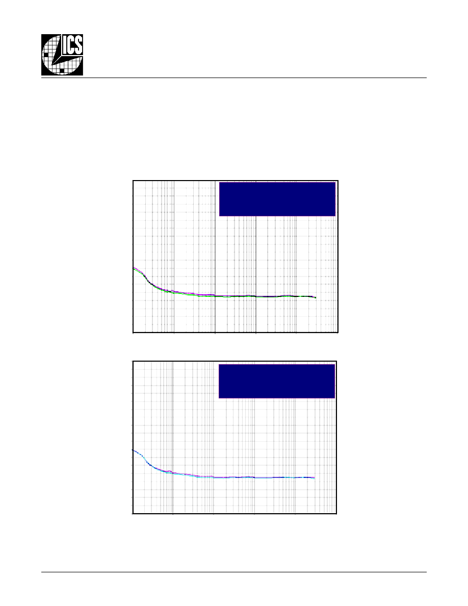
The spectral purity in a band at a specific offset from the funda-
mental compared to the power of the fundamental is called the
dBc Phase Noise. This value is normally expressed using a
Phase noise plot and is most often the specified plot in many
applications. Phase noise is defined as the ratio of the noise
power present in a 1Hz band at a specified offset from the fun-
damental frequency to the power value of the fundamental. This
ratio is expressed in decibels (dBm) or a ratio of the power in
As with most timing specifications, phase noise measurements
have issues. The primary issue relates to the limitations of the
equipment. Often the noise floor of the equipment is higher than
the noise floor of the device. This is illustrated above. The de-
the 1Hz band to the power in the fundamental. When the re-
quired offset is specified, the phase noise is called a
dBc value,
which simply means dBm at a specified offset from the funda-
mental. By investigating jitter in the frequency domain, we get a
better understanding of its effects on the desired application over
the entire time record of the signal. It is mathematically possible
to calculate an expected bit error rate given a phase noise plot.
vice meets the noise floor of what is shown, but can actually be
lower. The phase noise is dependant on the input source and
measurement equipment.
Additive Phase Jitter, RMS
@
156.25MHz (12KHz to 20MHz)
= 0.01ps typical @ 2.5V
0
-10
-20
-30
-40
-50
-60
-70
-80
-90
-100
-110
-120
-130
-140
-150
-160
-170
-180
-190
1k
10k
100k
1M
10M
100M
O
FFSET
F
ROM
C
ARRIER
F
REQUENCY
(H
Z
)
SSB P
HASE
N
OISE
dBc/H
Z
0
-10
-20
-30
-40
-50
-60
-70
-80
-90
-100
-110
-120
-130
-140
-150
-160
-170
-180
-190
1k
10k
100k
1M
10M
100M
O
FFSET
F
ROM
C
ARRIER
F
REQUENCY
(H
Z
)
SSB P
HASE
N
OISE
dBc/H
Z
Additive Phase Jitter, RMS
@
156.25MHz (12KHz to 20MHz)
= 0.02ps typical @ 3.3V
83947AYI-147
http://www.icst.com/products/hiperclocks.html
REV. A SEPTEMBER 24, 2004
6
Integrated
Circuit
Systems, Inc.
ICS83947I-147
L
OW
S
KEW
, 1-
TO
-9
LVCMOS/LVTTL F
ANOUT
B
UFFER
t
PD
V
DD
2
V
DDO
2
P
ARAMETER
M
EASUREMENT
I
NFORMATION
2.5V O
UTPUT
L
OAD
AC T
EST
C
IRCUIT
3.3V O
UTPUT
L
OAD
AC T
EST
C
IRCUIT
SCOPE
Qx
LVCMOS
1.65V ± 0.15V
-1.65V ± 0.15V
SCOPE
Qx
LVCMOS
1.25V±5%
-1.25V±5%
P
ART
-
TO
-P
ART
S
KEW
P
ROPAGATION
D
ELAY
O
UTPUT
D
UTY
C
YCLE
/P
ULSE
W
IDTH
/P
ERIOD
Clock
Outputs
0.8V
2V
2V
0.8V
t
R
t
F
tsk(o)
V
DDO
2
V
DDO
2
Qx
Qy
O
UTPUT
S
KEW
tsk(pp)
V
DDO
2
V
DDO
2
Qx
Qy
PART 1
PART 2
CLK0,CLK1
Q0:Q8
Q0:Q8
3.3V O
UTPUT
R
ISE
/F
ALL
T
IME
Clock
Outputs
20%
80%
80%
20%
t
R
t
F
t
PW
t
PERIOD
V
DDO
2
V
DDO
2
V
DDO
2
t
PW
t
PERIOD
odc =
V
DD
,
V
DDO
V
DD
,
V
DDO
2.5V O
UTPUT
R
ISE
/F
ALL
T
IME
GND
GND
83947AYI-147
http://www.icst.com/products/hiperclocks.html
REV. A SEPTEMBER 24, 2004
7
Integrated
Circuit
Systems, Inc.
ICS83947I-147
L
OW
S
KEW
, 1-
TO
-9
LVCMOS/LVTTL F
ANOUT
B
UFFER
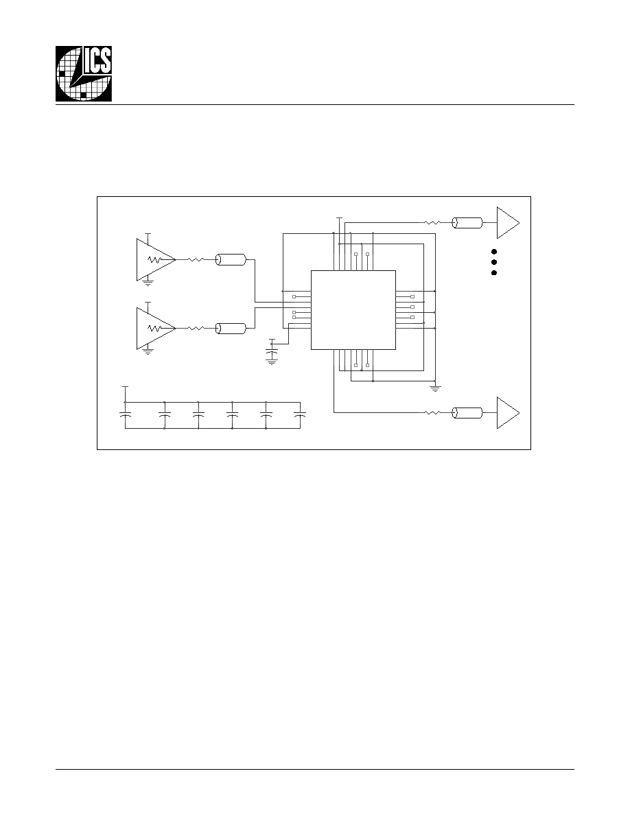
A
PPLICATION
S
CHEMATIC
E
XAMPLE
Figure 1 shows an example of ICS83947I-147 application sche-
matic. In this example, the device is operated at V
CC
=3.3V. The
decoupling capacitors should be located as close as possible
to the power pin. The input is driven by a 3.3V LVCMOS driver.
C4
0.1u
VCC
Zo = 50 Ohm
R3
43
R2
43
R1
43
C2
0.1u
(U1-22)
C3
0.1u
C1
0.1u
C3
0.1u
(U1-10)
VDDO
(U1-18)
C5
0.1u
VDDO
(U1-14)
Zo = 50
U1
ICS83947I-147
1
2
3
4
5
6
7
8
9
10
11
12
13
14
15
16
17
18
19
20
21
22
23
24
32
31
30
29
28
27
26
25
GND
CLK_SEL
CLK0
CLK1
CLK_EN
OE
VDD
GND
GN
D
V
DDO
Q8
GN
D
Q7
V
DDO
Q6
GN
D
GND
VDDO
Q5
GND
Q4
VDDO
Q3
GND
GN
D
V
DDO
Q0
GN
D
Q1
V
DDO
Q2
GN
D
VCC
VDD=3.3V
LVCMOS
Zo = 50
Zo = 50 Ohm
(U1-27)
VDD
VDDO=3.3V
LVCMOS
C2
0.1u
(U1-31)
R3
43
For the LVCMOS output drivers, only one termination example
is shown in this schematic. Additional termination approaches
are shown in the LVCMOS Termination Application Note (refer
to ICS website).
F
IGURE
1. ICS83947I-147 S
CHEMATIC
L
AYOUT

83947AYI-147
http://www.icst.com/products/hiperclocks.html
REV. A SEPTEMBER 24, 2004
8
Integrated
Circuit
Systems, Inc.
ICS83947I-147
L
OW
S
KEW
, 1-
TO
-9
LVCMOS/LVTTL F
ANOUT
B
UFFER
R
ELIABILITY
I
NFORMATION
T
RANSISTOR
C
OUNT
The transistor count for ICS83947I-147 is: 1040
T
ABLE
6.
JA
VS
. A
IR
F
LOW
T
ABLE
FOR
32 L
EAD
LQFP
JA
by Velocity (Linear Feet per Minute)
0
200
500
Single-Layer PCB, JEDEC Standard Test Boards
67.8∞C/W
55.9∞C/W
50.1∞C/W
Multi-Layer PCB, JEDEC Standard Test Boards
47.9∞C/W
42.1∞C/W
39.4∞C/W
NOTE: Most modern PCB designs use multi-layered boards. The data in the second row pertains to most designs.
83947AYI-147
http://www.icst.com/products/hiperclocks.html
REV. A SEPTEMBER 24, 2004
9
Integrated
Circuit
Systems, Inc.
ICS83947I-147
L
OW
S
KEW
, 1-
TO
-9
LVCMOS/LVTTL F
ANOUT
B
UFFER
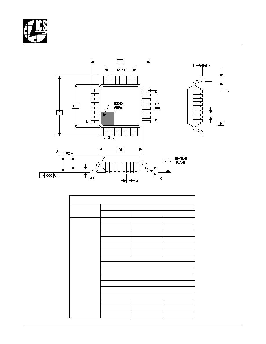
P
ACKAGE
O
UTLINE
- Y S
UFFIX
FOR
32 L
EAD
LQFP
T
ABLE
7. P
ACKAGE
D
IMENSIONS
N
O
I
T
A
I
R
A
V
C
E
D
E
J
S
R
E
T
E
M
I
L
L
I
M
N
I
S
N
O
I
S
N
E
M
I
D
L
L
A
L
O
B
M
Y
S
A
B
B
M
U
M
I
N
I
M
L
A
N
I
M
O
N
M
U
M
I
X
A
M
N
2
3
A
-
-
-
-
0
6
.
1
1
A
5
0
.
0
-
-
5
1
.
0
2
A
5
3
.
1
0
4
.
1
5
4
.
1
b
0
3
.
0
7
3
.
0
5
4
.
0
c
9
0
.
0
-
-
0
2
.
0
D
C
I
S
A
B
0
0
.
9
1
D
C
I
S
A
B
0
0
.
7
2
D
.
f
e
R
0
6
.
5
E
C
I
S
A
B
0
0
.
9
1
E
C
I
S
A
B
0
0
.
7
2
E
.
f
e
R
0
6
.
5
e
C
I
S
A
B
0
8
.
0
L
5
4
.
0
0
6
.
0
5
7
.
0
0
∞
-
-
7
∞
c
c
c
-
-
-
-
0
1
.
0
Reference Document: JEDEC Publication 95, MS-026

83947AYI-147
http://www.icst.com/products/hiperclocks.html
REV. A SEPTEMBER 24, 2004
10
Integrated
Circuit
Systems, Inc.
ICS83947I-147
L
OW
S
KEW
, 1-
TO
-9
LVCMOS/LVTTL F
ANOUT
B
UFFER
T
ABLE
8. O
RDERING
I
NFORMATION
While the information presented herein has been checked for both accuracy and reliability, Integrated Circuit Systems, Incorporated (ICS) assumes no responsibility for either its use
or for infringement of any patents or other rights of third parties, which would result from its use. No other circuits, patents, or licenses are implied. This product is intended for use
in normal commercial and industrial applications. Any other applications such as those requiring high reliability or other extraordinary environmental requirements are not
recommended without additional processing by ICS. ICS reserves the right to change any circuitry or specifications without notice. ICS does not authorize or warrant any ICS product
for use in life support devices or critical medical instruments.
r
e
b
m
u
N
r
e
d
r
O
/
t
r
a
P
g
n
i
k
r
a
M
e
g
a
k
c
a
P
t
n
u
o
C
e
r
u
t
a
r
e
p
m
e
T
7
4
1
-
I
Y
A
7
4
9
3
8
S
C
I
7
4
1
I
A
7
4
9
3
8
S
C
I
P
F
Q
L
d
a
e
L
2
3
y
a
r
t
r
e
p
0
5
2
C
∞
5
8
o
t
C
∞
0
4
-
T
7
4
1
-
I
Y
A
7
4
9
3
8
S
C
I
7
4
1
I
A
7
4
9
3
8
S
C
I
l
e
e
R
d
n
a
e
p
a
T
n
o
P
F
Q
L
d
a
e
L
2
3
0
0
0
1
C
∞
5
8
o
t
C
∞
0
4
-
The aforementioned trademark, HiPerClockSTM is a trademark of Integrated Circuit Systems, Inc. or its subsidiaries in the United States and/or other countries.