Document Outline
- General Description
- Features
- Frequency Select Function Table
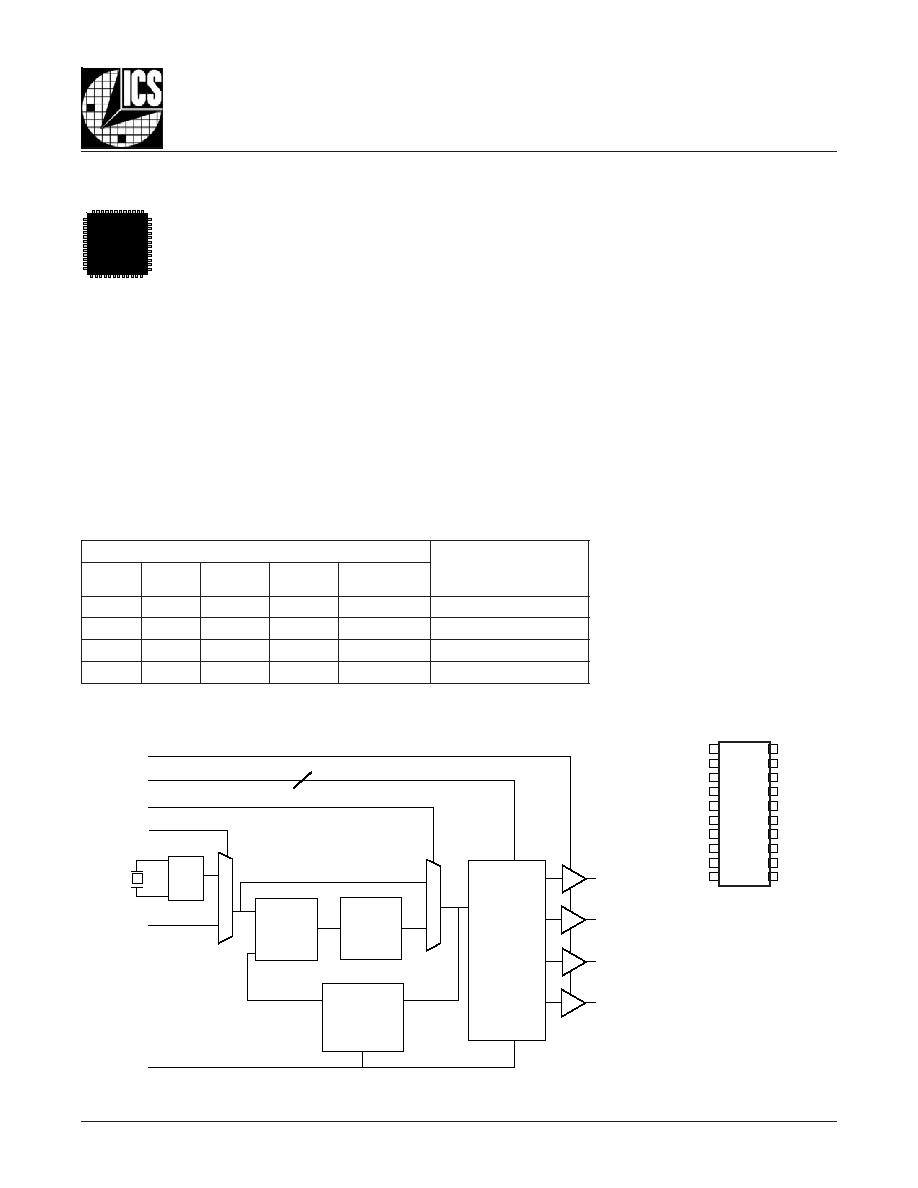
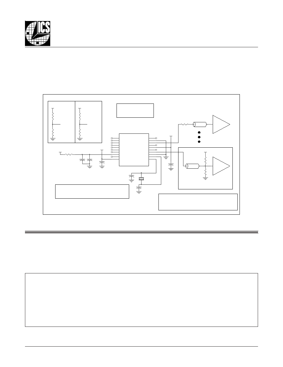
- Block Diagram
- Pin Assignment
- Pin Descriptions
- Pin Characteristics
- Absolute Maximum Ratings
- 3.3V Power Supply DC Characteristics
- 3.3V/2.5V Power Supply DC Characteristics
- 2.5V Power Supply DC Characteristics
- LVCMOS DC Characteristics
- Crystal Characteristics
- 3.3V AC Characteristics
- 3.3V/2.5V AC Characteristics
- 2.5V AC Characteristics
- Parameter Measurement Information
- 3.3V Core/3.3V Output Load AC Test Circuit Diagram
- 3.3V Core/2.5V Output Load AC Test Circuit Diagram
- 2.5V Core/2.5V Output Load AC Test Circuit Diagram
- RMS Phase Jitter Diagram
- Output Skew Diagram
- Output Rise/Fall Time Diagram
- Output Duty Cycle/Pulse Width/Period Diagram
- Application Information
- Power Supply Filtering Techniques
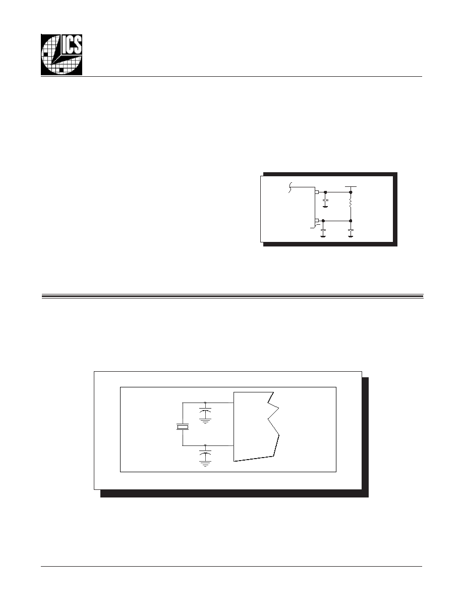
- Crystal Input Interface
- Layout Guideline
- Reliability Information
- Transistor Count
- Package Outline
- Package Dimensions
- Ordering Information
Integrated
Circuit
Systems, Inc.
840004AGI-01
www.icst.com/products/hiperclocks.html
REV. A JUNE 28, 2005
1
ICS840004I-01
F
EMTO
C
LOCKS
TM C
RYSTAL
-
TO
-
LVCMOS/LVTTL F
REQUENCY
S
YNTHESIZER
PRELIMINARY
G
ENERAL
D
ESCRIPTION
The ICS840004I-01 is a 4 output LVCMOS/LVTTL
Synthesizer optimized to generate Ethernet
reference clock frequencies and is a member of
the HiPerClocks
TM
family of high performance
clock solutions from ICS. Using a 25MHz, 18pF
parallel resonant crystal, the following frequencies can be
generated based on the 2 frequency select pins (F_SEL1:0):
156.25MHz, 125MHz, and 62.5MHz. The ICS840004I-01 uses
ICS' 3
rd
generation low phase noise VCO technology and can
achieve 1ps or lower typical random rms phase jitter, easily
meeting Ethernet jitter requirements. The ICS840004I-01 is
packaged in a small 20-pin TSSOP package.
HiPerClockSTM
ICS
B
LOCK
D
IAGRAM
F
EATURES
∑ Four LVCMOS/LVTTL outputs, 15
typical output impedance
∑ Selectable crystal oscillator interface
or LVCMOS single-ended input
∑ Supports the following output frequencies:
156.25MHz, 125MHz and 62.5MHz
∑ RMS phase jitter @ 156.25MHZ (1.875MHz - 20MHz):
0.52ps (typical)
∑ Output supply modes:
Core/Output
3.3V/3.3V
3.3V/2.5V
2.5V/2.5V
∑ -40∞C to 85∞C ambient operating temperature
Q0
Q1
Q2
Q3
OE
F_SEL1:0
nPLL_SEL
nXTAL_SEL
XTAL_IN
XTAL_OUT
TEST_CLK
MR
OSC
Phase
Detector
VCO
M = ˜25 (fixed)
F_SEL1:0
0 0 ˜4
0 1 ˜5
1 0 ˜10
1 1 ˜5
0
1
1
0
2
N
25MHz
Pullup
Pulldown
Pulldown
Pulldown
Pullup:Pullup
Pulldown
F
REQUENCY
S
ELECT
F
UNCTION
T
ABLE
P
IN
A
SSIGNMENT
ICS840004I-01
20-Lead TSSOP
6.5mm x 4.4mm x 0.92mm
package body
G Package
Top View
F_SEL0
nc
nXTAL_SEL
TEST_CLK
OE
MR
nPLL_SEL
V
DDA
nc
V
DD
1
2
3
4
5
6
7
8
9
10
20
19
18
17
16
15
14
13
12
11
F_SEL1
GND
Q0
Q1
V
DDO
Q2
Q3
GND
XTAL_IN
XTAL_OUT
s
t
u
p
n
I
)
z
H
M
(
y
c
n
e
u
q
e
r
F
t
u
p
t
u
O
)
.
f
e
R
z
H
M
5
2
(
1
L
E
S
_
F
0
L
E
S
_
F
r
e
d
i
v
i
D
M
e
u
l
a
V
r
e
d
i
v
i
D
N
e
u
l
a
V
N
/
M
e
u
l
a
V
o
i
t
a
R
0
0
5
2
4
5
2
.
6
5
2
.
6
5
1
0
1
5
2
5
5
5
2
1
1
0
5
2
0
1
5
.
2
5
.
2
6
1
1
5
2
5
5
5
2
1
The Preliminary Information presented herein represents a product in prototyping or pre-production. The noted characteristics are based on initial
product characterization. Integrated Circuit Systems, Incorporated (ICS) reserves the right to change any circuitry or specifications without notice.

Integrated
Circuit
Systems, Inc.
840004AGI-01
www.icst.com/products/hiperclocks.html
REV. A JUNE 28, 2005
2
ICS840004I-01
F
EMTO
C
LOCKS
TM C
RYSTAL
-
TO
-
LVCMOS/LVTTL F
REQUENCY
S
YNTHESIZER
PRELIMINARY
T
ABLE
1. P
IN
D
ESCRIPTIONS
T
ABLE
2. P
IN
C
HARACTERISTICS
r
e
b
m
u
N
e
m
a
N
e
p
y
T
n
o
i
t
p
i
r
c
s
e
D
0
2
,
1
,
0
L
E
S
_
F
1
L
E
S
_
F
t
u
p
n
I
p
u
ll
u
P
.
s
l
e
v
e
l
e
c
a
f
r
e
t
n
i
L
T
T
V
L
/
S
O
M
C
V
L
.
n
i
p
t
c
e
l
e
s
y
c
n
e
u
q
e
r
F
9
,
2
c
n
d
e
s
u
n
U
.
t
c
e
n
n
o
c
o
N
3
L
E
S
_
L
A
T
X
n
t
u
p
n
I
n
w
o
d
ll
u
P
e
c
n
e
r
e
f
e
r
L
L
P
e
h
t
s
a
s
t
u
p
n
i
K
L
C
_
T
S
E
T
r
o
l
a
t
s
y
r
c
e
h
t
n
e
e
w
t
e
b
s
t
c
e
l
e
S
L
A
T
X
s
t
c
e
l
e
s
,
W
O
L
n
e
h
W
.
K
L
C
_
T
S
E
T
s
t
c
e
l
e
s
,
H
G
I
H
n
e
h
W
.
e
c
r
u
o
s
.
s
l
e
v
e
l
e
c
a
f
r
e
t
n
i
L
T
T
V
L
/
S
O
M
C
V
L
.
s
u
p
n
i
4
K
L
C
_
T
S
E
T
t
u
p
n
I
n
w
o
d
ll
u
P
.
t
u
p
n
i
k
c
o
l
c
L
T
T
V
L
/
S
O
M
C
V
L
d
e
d
n
e
-
e
l
g
n
i
S
5
E
O
t
u
p
n
I
p
u
ll
u
P
e
h
t
,
W
O
L
n
e
h
W
.
e
v
i
t
c
a
e
r
a
s
t
u
p
t
u
o
e
h
t
,
H
G
I
H
n
e
h
W
.
n
i
p
e
l
b
a
n
e
t
u
p
t
u
O
.
s
l
e
v
e
l
e
c
a
f
r
e
t
n
i
L
T
T
V
L
/
S
O
M
C
V
L
.
e
t
a
t
s
e
c
n
a
d
e
p
m
i
h
g
i
h
a
n
i
e
r
a
s
t
u
p
t
u
o
6
R
M
t
u
p
n
I
n
w
o
d
ll
u
P
e
r
a
s
r
e
d
i
v
i
d
l
a
n
r
e
t
n
i
e
h
t
,
H
G
I
H
c
i
g
o
l
n
e
h
W
.
t
e
s
e
R
r
e
t
s
a
M
H
G
I
H
e
v
i
t
c
A
l
a
n
r
e
t
n
i
e
h
t
,
W
O
L
c
i
g
o
l
n
e
h
W
.
w
o
l
o
g
o
t
s
t
u
p
u
t
o
e
h
t
g
n
i
s
u
a
c
t
e
s
e
r
.
s
l
e
v
e
l
e
c
a
f
r
e
t
n
i
L
T
T
V
L
/
S
O
M
C
V
L
.
d
e
l
b
a
n
e
e
r
a
s
t
u
p
t
u
o
e
h
t
d
n
a
s
r
e
d
i
v
i
d
7
L
E
S
_
L
L
P
n
t
u
p
n
I
n
w
o
d
ll
u
P
.
t
u
p
t
u
o
O
C
V
e
h
t
m
o
r
f
n
e
v
i
r
d
s
i
t
u
p
t
u
o
e
h
t
,
W
O
L
n
e
h
W
.
s
s
a
p
y
B
L
L
P
=
y
c
n
e
u
q
e
r
f
t
u
p
t
u
o
e
h
t
d
n
a
d
e
s
s
a
p
y
b
s
i
L
L
P
e
h
t
,
H
G
I
H
n
e
h
W
.
r
e
d
i
v
i
d
t
u
p
t
u
o
N
/
y
c
n
e
u
q
e
r
f
k
c
o
l
c
e
c
n
e
r
e
f
e
r
.
s
l
e
v
e
l
e
c
a
f
r
e
t
n
i
L
T
T
V
L
/
S
O
M
C
V
L
8
V
A
D
D
r
e
w
o
P
.
n
i
p
y
l
p
p
u
s
g
o
l
a
n
A
0
1
V
D
D
r
e
w
o
P
.
n
i
p
y
l
p
p
u
s
e
r
o
C
,
1
1
2
1
,
T
U
O
_
L
A
T
X
N
I
_
L
A
T
X
t
u
p
n
I
.
t
u
p
t
u
o
e
h
t
s
i
T
U
O
_
L
A
T
X
.
e
c
a
f
r
e
t
n
i
r
o
t
a
ll
i
c
s
o
l
a
t
s
y
r
C
.
t
u
p
n
i
e
h
t
s
i
N
I
_
L
A
T
X
9
1
,
3
1
D
N
G
r
e
w
o
P
.
d
n
u
o
r
g
y
l
p
p
u
s
r
e
w
o
P
5
1
,
4
1
8
1
,
7
1
,
2
Q
,
3
Q
0
Q
,
1
Q
t
u
p
t
u
O
.
s
l
e
v
e
l
e
c
a
f
r
e
t
n
i
L
T
T
V
L
/
S
O
M
C
V
L
.
s
t
u
p
t
u
o
k
c
o
l
c
d
e
d
n
e
-
e
l
g
n
i
S
5
1
.
e
c
n
e
d
e
p
m
i
t
u
p
t
u
o
l
a
c
i
p
y
t
6
1
V
O
D
D
r
e
w
o
P
.
n
i
p
y
l
p
p
u
s
t
u
p
t
u
O
:
E
T
O
N
p
u
ll
u
P
d
n
a
n
w
o
d
ll
u
P
.
s
e
u
l
a
v
l
a
c
i
p
y
t
r
o
f
,
s
c
i
t
s
i
r
e
t
c
a
r
a
h
C
n
i
P
,
2
e
l
b
a
T
e
e
S
.
s
r
o
t
s
i
s
e
r
t
u
p
n
i
l
a
n
r
e
t
n
i
o
t
r
e
f
e
r
l
o
b
m
y
S
r
e
t
e
m
a
r
a
P
s
n
o
i
t
i
d
n
o
C
t
s
e
T
m
u
m
i
n
i
M
l
a
c
i
p
y
T
m
u
m
i
x
a
M
s
t
i
n
U
C
N
I
e
c
n
a
t
i
c
a
p
a
C
t
u
p
n
I
4
F
p
C
D
P
e
c
n
a
t
i
c
a
p
a
C
n
o
i
t
a
p
i
s
s
i
D
r
e
w
o
P
V
D
D
V
,
A
D
D
V
,
O
D
D
V
5
6
4
.
3
=
D
B
T
F
p
V
D
D
V
,
A
D
D
V
,
V
5
6
4
.
3
=
O
D
D
V
5
2
6
.
2
=
D
B
T
F
p
V
D
D
V
,
A
D
D
V
,
O
D
D
V
5
2
6
.
2
=
D
B
T
F
p
R
P
U
L
L
U
P
r
o
t
s
i
s
e
R
p
u
ll
u
P
t
u
p
n
I
1
5
k
R
N
W
O
D
L
L
U
P
r
o
t
s
i
s
e
R
n
w
o
d
ll
u
P
t
u
p
n
I
1
5
k
R
T
U
O
e
c
n
a
d
e
p
m
I
t
u
p
t
u
O
5
1
Integrated
Circuit
Systems, Inc.
840004AGI-01
www.icst.com/products/hiperclocks.html
REV. A JUNE 28, 2005
3
ICS840004I-01
F
EMTO
C
LOCKS
TM C
RYSTAL
-
TO
-
LVCMOS/LVTTL F
REQUENCY
S
YNTHESIZER
PRELIMINARY
T
ABLE
3A. P
OWER
S
UPPLY
DC C
HARACTERISTICS
,
V
DDD
= V
DDA
= 3.3V±5%, V
DDO
= 3.3V±5%
OR
2.5V±5%, T
A
= -40∞C
TO
85∞C
A
BSOLUTE
M
AXIMUM
R
ATINGS
Supply Voltage, V
DD
4.6V
Inputs, V
I
-0.5V to V
DD
+ 0.5 V
Outputs, V
O
-0.5V to V
DD
+ 0.5V
Package Thermal Impedance,
JA
73.2∞C/W (0 lfpm)
Storage Temperature, T
STG
-65∞C to 150∞C
NOTE: Stresses beyond those listed under Absolute
Maximum Ratings may cause permanent damage to the
device. These ratings are stress specifications only. Functional
operation of product at these conditions or any conditions be-
yond those listed in the
DC Characteristics or AC Character-
istics is not implied. Exposure to absolute maximum rating
conditions for extended periods may affect product reliability.
l
o
b
m
y
S
r
e
t
e
m
a
r
a
P
s
n
o
i
t
i
d
n
o
C
t
s
e
T
m
u
m
i
n
i
M
l
a
c
i
p
y
T
m
u
m
i
x
a
M
s
t
i
n
U
V
D
D
e
g
a
t
l
o
V
y
l
p
p
u
S
e
r
o
C
5
3
1
.
3
3
.
3
5
6
4
.
3
V
V
A
D
D
e
g
a
t
l
o
V
y
l
p
p
u
S
g
o
l
a
n
A
5
3
1
.
3
3
.
3
5
6
4
.
3
V
V
O
D
D
e
g
a
t
l
o
V
y
l
p
p
u
S
t
u
p
t
u
O
5
3
1
.
3
3
.
3
5
6
4
.
3
V
5
7
3
.
2
5
.
2
5
2
6
.
2
V
I
D
D
t
n
e
r
r
u
C
y
l
p
p
u
S
r
e
w
o
P
0
9
A
m
I
A
D
D
t
n
e
r
r
u
C
y
l
p
p
u
S
g
o
l
a
n
A
8
A
m
I
O
D
D
t
n
e
r
r
u
C
y
l
p
p
u
S
t
u
p
t
u
O
5
A
m
T
ABLE
3B. P
OWER
S
UPPLY
DC C
HARACTERISTICS
,
V
DD
= V
DDA
= V
DDO
= 2.5V±5%, T
A
= -40∞C
TO
85∞C
l
o
b
m
y
S
r
e
t
e
m
a
r
a
P
s
n
o
i
t
i
d
n
o
C
t
s
e
T
m
u
m
i
n
i
M
l
a
c
i
p
y
T
m
u
m
i
x
a
M
s
t
i
n
U
V
D
D
e
g
a
t
l
o
V
y
l
p
p
u
S
e
r
o
C
5
7
3
.
2
5
.
2
5
2
6
.
2
V
V
A
D
D
e
g
a
t
l
o
V
y
l
p
p
u
S
g
o
l
a
n
A
5
7
3
.
2
5
.
2
5
2
6
.
2
V
V
O
D
D
e
g
a
t
l
o
V
y
l
p
p
u
S
t
u
p
t
u
O
5
7
3
.
2
5
.
2
5
2
6
.
2
V
I
D
D
t
n
e
r
r
u
C
y
l
p
p
u
S
r
e
w
o
P
0
8
A
m
I
A
D
D
t
n
e
r
r
u
C
y
l
p
p
u
S
g
o
l
a
n
A
8
A
m
I
O
D
D
t
n
e
r
r
u
C
y
l
p
p
u
S
t
u
p
t
u
O
5
A
m
Integrated
Circuit
Systems, Inc.
840004AGI-01
www.icst.com/products/hiperclocks.html
REV. A JUNE 28, 2005
4
ICS840004I-01
F
EMTO
C
LOCKS
TM C
RYSTAL
-
TO
-
LVCMOS/LVTTL F
REQUENCY
S
YNTHESIZER
PRELIMINARY
T
ABLE
5A. AC C
HARACTERISTICS
,
V
DD
= V
DDA
= V
DDO
= 3.3V±5%, T
A
= -40∞C
TO
85∞C
T
ABLE
4. C
RYSTAL
C
HARACTERISTICS
r
e
t
e
m
a
r
a
P
s
n
o
i
t
i
d
n
o
C
t
s
e
T
m
u
m
i
n
i
M
l
a
c
i
p
y
T
m
u
m
i
x
a
M
s
t
i
n
U
n
o
i
t
a
ll
i
c
s
O
f
o
e
d
o
M
l
a
t
n
e
m
a
d
n
u
F
y
c
n
e
u
q
e
r
F
5
2
z
H
M
)
R
S
E
(
e
c
n
a
t
s
i
s
e
R
s
e
i
r
e
S
t
n
e
l
a
v
i
u
q
E
0
5
e
c
n
a
t
i
c
a
p
a
C
t
n
u
h
S
7
F
p
l
e
v
e
L
e
v
i
r
D
1
W
m
.
l
a
t
s
y
r
c
t
n
a
n
o
s
e
r
l
e
ll
a
r
a
p
f
p
8
1
n
a
g
n
i
s
u
d
e
z
i
r
e
t
c
a
r
a
h
C
:
E
T
O
N
T
ABLE
3C. LVCMOS/LVTTL DC C
HARACTERISTICS
,
V
DD
= V
DDA
= V
DDO
= 3.3V±5%
OR
2.5V±5%,
OR
V
DD
= V
DDA
= 3.3V±5%, V
DDO
= 2.5V±5%, T
A
= -40∞C
TO
85∞C
l
o
b
m
y
S
r
e
t
e
m
a
r
a
P
s
n
o
i
t
i
d
n
o
C
t
s
e
T
m
u
m
i
n
i
M
l
a
c
i
p
y
T
m
u
m
i
x
a
M
s
t
i
n
U
V
H
I
e
g
a
t
l
o
V
h
g
i
H
t
u
p
n
I
V
D
D
V
3
.
3
=
2
V
D
D
3
.
0
+
V
V
D
D
V
5
.
2
=
7
.
1
V
D
D
3
.
0
+
V
V
L
I
e
g
a
t
l
o
V
w
o
L
t
u
p
n
I
V
D
D
V
3
.
3
=
3
.
0
-
8
.
0
V
V
D
D
V
5
.
2
=
3
.
0
-
7
.
0
V
I
H
I
t
u
p
n
I
t
n
e
r
r
u
C
h
g
i
H
1
:
0
L
E
S
_
F
,
E
O
V
D
D
V
=
N
I
r
o
V
5
6
4
.
3
=
V
5
2
6
.
2
5
A
µ
,
R
M
,
L
E
S
_
L
L
P
n
K
L
C
_
T
S
E
T
,
L
E
S
_
L
A
T
X
n
V
D
D
V
=
N
I
r
o
V
5
6
4
.
3
=
V
5
2
6
.
2
0
5
1
A
µ
I
L
I
t
u
p
n
I
t
n
e
r
r
u
C
w
o
L
1
:
0
L
E
S
_
F
,
E
O
V
D
D
,
V
5
.
2
r
o
V
5
6
4
.
3
=
V
N
I
V
0
=
0
5
1
-
A
µ
,
R
M
,
L
E
S
_
L
L
P
n
K
L
C
_
T
S
E
T
,
L
E
S
_
L
A
T
X
n
V
D
D
,
V
5
.
2
r
o
V
5
6
4
.
3
=
V
N
I
V
0
=
5
-
A
µ
V
H
O
1
E
T
O
N
;
e
g
a
t
l
o
V
h
g
i
H
t
u
p
t
u
O
V
O
D
D
%
5
±
V
3
.
3
=
6
.
2
V
V
O
D
D
%
5
±
V
5
.
2
=
8
.
1
V
V
L
O
1
E
T
O
N
;
e
g
a
t
l
o
V
w
o
L
t
u
p
t
u
O
V
O
D
D
%
5
±
V
5
.
2
r
o
V
3
.
3
=
5
.
0
V
0
5
h
t
i
w
d
e
t
a
n
i
m
r
e
t
s
t
u
p
t
u
O
:
1
E
T
O
N
V
o
t
O
D
D
.
t
i
u
c
r
i
C
t
s
e
T
d
a
o
L
t
u
p
t
u
O
,
n
o
i
t
a
m
r
o
f
n
I
t
n
e
m
e
r
u
s
a
e
M
r
e
t
e
m
a
r
a
P
e
e
S
.
2
/
l
o
b
m
y
S
r
e
t
e
m
a
r
a
P
s
n
o
i
t
i
d
n
o
C
t
s
e
T
m
u
m
i
n
i
M
l
a
c
i
p
y
T
m
u
m
i
x
a
M
s
t
i
n
U
f
T
U
O
y
c
n
e
u
q
e
r
F
t
u
p
t
u
O
5
2
.
6
5
1
z
H
M
5
2
1
z
H
M
5
.
2
6
z
H
M
t
)
o
(
k
s
2
,
1
E
T
O
N
;
w
e
k
S
t
u
p
t
u
O
D
B
T
s
p
t
)
ÿ
(
t
ij
;
)
m
o
d
n
a
R
(
r
e
t
t
i
J
e
s
a
h
P
S
M
R
3
E
T
O
N
)
z
H
M
0
2
-
z
H
M
5
7
8
.
1
(
,
z
H
M
5
2
.
6
5
1
2
5
.
0
s
p
)
z
H
M
0
2
-
z
H
M
5
7
8
.
1
(
,
z
H
M
5
2
1
5
6
.
0
s
p
)
z
H
M
0
2
-
z
H
M
5
7
8
.
1
(
,
z
H
M
5
.
2
6
5
5
.
0
s
p
t
L
e
m
i
T
k
c
o
L
L
L
P
D
B
T
s
m
t
R
t
/
F
e
m
i
T
ll
a
F
/
e
s
i
R
t
u
p
t
u
O
%
0
8
o
t
%
0
2
0
0
4
s
p
c
d
o
e
l
c
y
C
y
t
u
D
t
u
p
t
u
O
0
5
%
.
s
n
o
i
t
i
d
n
o
c
d
a
o
l
l
a
u
q
e
h
t
i
w
d
n
a
s
e
g
a
t
l
o
v
y
l
p
p
u
s
e
m
a
s
e
h
t
t
a
s
t
u
p
t
u
o
n
e
e
w
t
e
b
w
e
k
s
s
a
d
e
n
i
f
e
D
:
1
E
T
O
N
V
t
a
d
e
r
u
s
a
e
M
O
D
D
.
2
/
.
5
6
d
r
a
d
n
a
t
S
C
E
D
E
J
h
t
i
w
e
c
n
a
d
r
o
c
c
a
n
i
d
e
n
i
f
e
d
s
i
r
e
t
e
m
a
r
a
p
s
i
h
T
:
2
E
T
O
N
.
t
o
l
P
e
s
i
o
N
e
s
a
h
P
e
h
t
o
t
r
e
f
e
r
e
s
a
e
l
P
:
3
E
T
O
N

Integrated
Circuit
Systems, Inc.
840004AGI-01
www.icst.com/products/hiperclocks.html
REV. A JUNE 28, 2005
5
ICS840004I-01
F
EMTO
C
LOCKS
TM C
RYSTAL
-
TO
-
LVCMOS/LVTTL F
REQUENCY
S
YNTHESIZER
PRELIMINARY
T
ABLE
5B. AC C
HARACTERISTICS
,
V
DD
= V
DDA
= 3.3V±5%, V
DDO
= 2.5V±5%, T
A
= -40∞C
TO
85∞C
l
o
b
m
y
S
r
e
t
e
m
a
r
a
P
s
n
o
i
t
i
d
n
o
C
t
s
e
T
m
u
m
i
n
i
M
l
a
c
i
p
y
T
m
u
m
i
x
a
M
s
t
i
n
U
f
T
U
O
y
c
n
e
u
q
e
r
F
t
u
p
t
u
O
5
2
.
6
5
1
z
H
M
5
2
1
z
H
M
5
.
2
6
z
H
M
t
)
o
(
k
s
2
,
1
E
T
O
N
;
w
e
k
S
t
u
p
t
u
O
D
B
T
s
p
t
)
ÿ
(
t
ij
;
)
m
o
d
n
a
R
(
r
e
t
t
i
J
e
s
a
h
P
S
M
R
3
E
T
O
N
)
z
H
M
0
2
-
z
H
M
5
7
8
.
1
(
,
z
H
M
5
2
.
6
5
1
8
4
.
0
s
p
)
z
H
M
0
2
-
z
H
M
5
7
8
.
1
(
,
z
H
M
5
2
1
9
5
.
0
s
p
)
z
H
M
0
2
-
z
H
M
5
7
8
.
1
(
,
z
H
M
5
.
2
6
3
5
.
0
s
p
t
L
e
m
i
T
k
c
o
L
L
L
P
D
B
T
s
m
t
R
t
/
F
e
m
i
T
ll
a
F
/
e
s
i
R
t
u
p
t
u
O
%
0
8
o
t
%
0
2
0
5
4
s
p
c
d
o
e
l
c
y
C
y
t
u
D
t
u
p
t
u
O
0
5
%
.
s
n
o
i
t
i
d
n
o
c
d
a
o
l
l
a
u
q
e
h
t
i
w
d
n
a
s
e
g
a
t
l
o
v
y
l
p
p
u
s
e
m
a
s
e
h
t
t
a
s
t
u
p
t
u
o
n
e
e
w
t
e
b
w
e
k
s
s
a
d
e
n
i
f
e
D
:
1
E
T
O
N
V
t
a
d
e
r
u
s
a
e
M
O
D
D
.
2
/
.
5
6
d
r
a
d
n
a
t
S
C
E
D
E
J
h
t
i
w
e
c
n
a
d
r
o
c
c
a
n
i
d
e
n
i
f
e
d
s
i
r
e
t
e
m
a
r
a
p
s
i
h
T
:
2
E
T
O
N
.
t
o
l
P
e
s
i
o
N
e
s
a
h
P
e
h
t
o
t
r
e
f
e
r
e
s
a
e
l
P
:
3
E
T
O
N
T
ABLE
5C. AC C
HARACTERISTICS
,
V
DD
= V
DDA
= V
DDO
= 2.5V±5%, T
A
= -40∞C
TO
85∞C
l
o
b
m
y
S
r
e
t
e
m
a
r
a
P
s
n
o
i
t
i
d
n
o
C
t
s
e
T
m
u
m
i
n
i
M
l
a
c
i
p
y
T
m
u
m
i
x
a
M
s
t
i
n
U
f
T
U
O
y
c
n
e
u
q
e
r
F
t
u
p
t
u
O
5
2
.
6
5
1
z
H
M
5
2
1
z
H
M
5
.
2
6
z
H
M
t
)
o
(
k
s
2
,
1
E
T
O
N
;
w
e
k
S
t
u
p
t
u
O
D
B
T
s
p
t
)
ÿ
(
t
ij
;
)
m
o
d
n
a
R
(
r
e
t
t
i
J
e
s
a
h
P
S
M
R
3
E
T
O
N
)
z
H
M
0
2
-
z
H
M
5
7
8
.
1
(
,
z
H
M
5
2
.
6
5
1
0
5
.
0
s
p
)
z
H
M
0
2
-
z
H
M
5
7
8
.
1
(
,
z
H
M
5
2
1
0
6
.
0
s
p
)
z
H
M
0
2
-
z
H
M
5
7
8
.
1
(
,
z
H
M
5
.
2
6
1
5
.
0
s
p
t
L
e
m
i
T
k
c
o
L
L
L
P
D
B
T
s
m
t
R
t
/
F
e
m
i
T
ll
a
F
/
e
s
i
R
t
u
p
t
u
O
%
0
8
o
t
%
0
2
0
5
4
s
p
c
d
o
e
l
c
y
C
y
t
u
D
t
u
p
t
u
O
0
5
%
.
s
n
o
i
t
i
d
n
o
c
d
a
o
l
l
a
u
q
e
h
t
i
w
d
n
a
s
e
g
a
t
l
o
v
y
l
p
p
u
s
e
m
a
s
e
h
t
t
a
s
t
u
p
t
u
o
n
e
e
w
t
e
b
w
e
k
s
s
a
d
e
n
i
f
e
D
:
1
E
T
O
N
V
t
a
d
e
r
u
s
a
e
M
O
D
D
.
2
/
.
5
6
d
r
a
d
n
a
t
S
C
E
D
E
J
h
t
i
w
e
c
n
a
d
r
o
c
c
a
n
i
d
e
n
i
f
e
d
s
i
r
e
t
e
m
a
r
a
p
s
i
h
T
:
2
E
T
O
N
.
t
o
l
P
e
s
i
o
N
e
s
a
h
P
e
h
t
o
t
r
e
f
e
r
e
s
a
e
l
P
:
3
E
T
O
N

Integrated
Circuit
Systems, Inc.
840004AGI-01
www.icst.com/products/hiperclocks.html
REV. A JUNE 28, 2005
6
ICS840004I-01
F
EMTO
C
LOCKS
TM C
RYSTAL
-
TO
-
LVCMOS/LVTTL F
REQUENCY
S
YNTHESIZER
PRELIMINARY
P
ARAMETER
M
EASUREMENT
I
NFORMATION
t
PERIOD
t
PW
t
PERIOD
odc =
V
DDO
2
x 100%
t
PW
Q0:Q3
RMS P
HASE
J
ITTER
O
UTPUT
S
KEW
3.3V C
ORE
/3.3V O
UTPUT
L
OAD
AC T
EST
C
IRCUIT
SCOPE
Qx
LVCMOS
1.65V±5%
-1.65V±5%
O
UTPUT
D
UTY
C
YCLE
/P
ULSE
W
IDTH
/P
ERIOD
Clock
Outputs
20%
80%
80%
20%
t
R
t
F
V
DD
,
V
DDA
, V
DDO
GND
Phase Noise Mask
Offset Frequency
f
1
f
2
Phase Noise Plot
RMS Jitter = Area Under the Masked Phase Noise Plot
Noise P
o
w
er
tsk(o)
V
DDO
2
V
DDO
2
Qx
Qy
O
UTPUT
R
ISE
/F
ALL
T
IME
SCOPE
Qx
LVCMOS
2.05V±5%
-1.25V±5%
V
DD
,
V
DDA
GND
1.25V±5%
V
DDO
3.3V C
ORE
/2.5V O
UTPUT
L
OAD
AC T
EST
C
IRCUIT
2.5V C
ORE
/2.5V O
UTPUT
L
OAD
AC T
EST
C
IRCUIT
SCOPE
Qx
LVCMOS
1.25V±5%
-1.25V±5%
V
DD
,
V
DDA
, V
DDO
GND
Integrated
Circuit
Systems, Inc.
840004AGI-01
www.icst.com/products/hiperclocks.html
REV. A JUNE 28, 2005
7
ICS840004I-01
F
EMTO
C
LOCKS
TM C
RYSTAL
-
TO
-
LVCMOS/LVTTL F
REQUENCY
S
YNTHESIZER
PRELIMINARY
A
PPLICATION
I
NFORMATION
As in any high speed analog circuitry, the power supply pins
are vulnerable to random noise. The ICS840004I-01 provides
separate power supplies to isolate any high switching
noise from the outputs to the internal PLL. V
DD
, V
DDA
, and V
DDO
should be individually connected to the power supply
plane through vias, and bypass capacitors should be
used for each pin. To achieve optimum jitter performance,
power supply isolation is required.
Figure 1 illustrates how
a 10
resistor along with a 10µF and a .01F bypass
capacitor should be connected to each V
DDA
.
P
OWER
S
UPPLY
F
ILTERING
T
ECHNIQUES
F
IGURE
1. P
OWER
S
UPPLY
F
ILTERING
10
V
DDA
10
F
.01
F
3.3V or 2.5V
.01
F
V
DD
C
RYSTAL
I
NPUT
I
NTERFACE
The ICS840004I-01 has been characterized with 18pF paral-
lel resonant crystals. The capacitor values shown in
Figure 2
Figure 2. C
RYSTAL
I
NPU
t I
NTERFACE
below were determined using a 25MHz 18pF parallel reso-
nant crystal and were chosen to minimize the ppm error.
ICS84332
XTAL_IN
XTAL_OUT
X1
18pF Parallel Cry stal
C2
22p
C1
22p
ICS840004I-01
Integrated
Circuit
Systems, Inc.
840004AGI-01
www.icst.com/products/hiperclocks.html
REV. A JUNE 28, 2005
8
ICS840004I-01
F
EMTO
C
LOCKS
TM C
RYSTAL
-
TO
-
LVCMOS/LVTTL F
REQUENCY
S
YNTHESIZER
PRELIMINARY
R
ELIABILITY
I
NFORMATION
T
RANSISTOR
C
OUNT
The transistor count for ICS840004I-01 is: TBD
T
ABLE
6.
JA
VS
. A
IR
F
LOW
T
ABLE
FOR
20 L
EAD
TSSOP
JA
by Velocity (Linear Feet per Minute)
0
200
500
Single-Layer PCB, JEDEC Standard Test Boards
114.5∞C/W
98.0∞C/W
88.0∞C/W
Multi-Layer PCB, JEDEC Standard Test Boards
73.2∞C/W
66.6∞C/W
63.5∞C/W
NOTE: Most modern PCB designs use multi-layered boards. The data in the second row pertains to most designs.
L
AYOUT
G
UIDELINE
Figure 3 shows a schematic example of the ICS840004I-01. An
example of LVCMOS termination is shown in this schematic.
Additional LVCMOS termination approaches are shown in the
LVCMOS Termination Application Note. In this example, an 18pF
parallel resonant 25MHz crystal is used. The C1=22pF and
F
IGURE
3. ICS840004I-01 S
CHEMATIC
E
XAMPLE
C2=22pF are recommended for frequency accuracy. For differ-
ent board layout, the C1 and C2 may be slightly adjusted for
optimizing frequency accuracy. 1K
pullup or pulldown resis-
tors can be used for the logic control input pins.
XTAL_IN
Unused outputs can be left floating. There should be
no trace attached to unused outputs. Device
characterized and specification limits set with all
outputs terminated.
RU1
1K
LVCMOS
VDDO=3.3V
R4
100
R3
36
Logic Control Input Examples
VDDA
C5
0.1u
VDD=3.3V
RD1
Not Install
VDD
X1
C3
10uF
To Logic
Input
pins
Optional Termination
VDD
Set Logic
Input to
'1'
R5
100
U1
ICS840004i-01
1
2
3
4
5
6
7
8
9
10
11
12
13
14
15
16
20
19
18
17
F_SEL0
nc
nXTAL_SEL
TEST_CLK
OE
MR
nPLL_SEL
VDDA
nc
VDD
XTAL_OUT
XTAL_IN
GND
Q3
Q2
VDDO
F_SEL1
GND
Q0
Q1
C2
22pF
C6
0.1u
VDDO
RU2
Not Install
LVCMOS
R2
10
Zo = 50 Ohm
VDD
VDD
VDD
RD2
1K
VDD
Set Logic
Input to
'0'
XTAL_OUT
C1
22pF
To Logic
Input
pins
If not using the crystal input, it can be left floating.
For additional protection the XTAL_IN pin can be
tied to ground.
C4
0.01u
Zo = 50 Ohm

Integrated
Circuit
Systems, Inc.
840004AGI-01
www.icst.com/products/hiperclocks.html
REV. A JUNE 28, 2005
9
ICS840004I-01
F
EMTO
C
LOCKS
TM C
RYSTAL
-
TO
-
LVCMOS/LVTTL F
REQUENCY
S
YNTHESIZER
PRELIMINARY
P
ACKAGE
O
UTLINE
- G S
UFFIX
FOR
20 L
EAD
TSSOP
T
ABLE
7. P
ACKAGE
D
IMENSIONS
L
O
B
M
Y
S
s
r
e
t
e
m
i
l
l
i
M
N
I
M
X
A
M
N
0
2
A
-
-
0
2
.
1
1
A
5
0
.
0
5
1
.
0
2
A
0
8
.
0
5
0
.
1
b
9
1
.
0
0
3
.
0
c
9
0
.
0
0
2
.
0
D
0
4
.
6
0
6
.
6
E
C
I
S
A
B
0
4
.
6
1
E
0
3
.
4
0
5
.
4
e
C
I
S
A
B
5
6
.
0
L
5
4
.
0
5
7
.
0
∞
0
∞
8
a
a
a
-
-
0
1
.
0
Reference Document: JEDEC Publication 95, MO-153
Integrated
Circuit
Systems, Inc.
840004AGI-01
www.icst.com/products/hiperclocks.html
REV. A JUNE 28, 2005
10
ICS840004I-01
F
EMTO
C
LOCKS
TM C
RYSTAL
-
TO
-
LVCMOS/LVTTL F
REQUENCY
S
YNTHESIZER
PRELIMINARY
T
ABLE
8. O
RDERING
I
NFORMATION
While the information presented herein has been checked for both accuracy and reliability, Integrated Circuit Systems, Incorporated (ICS) assumes no responsibility for either its use
or for infringement of any patents or other rights of third parties, which would result from its use. No other circuits, patents, or licenses are implied. This product is intended for use
in normal commercial and industrial applications. Any other applications such as those requiring high reliability or other extraordinary environmental requirements are not
recommended without additional processing by ICS. ICS reserves the right to change any circuitry or specifications without notice. ICS does not authorize or warrant any ICS product
for use in life support devices or critical medical instruments.
The aforementioned trademarks, HiPerClockS
and F
EMTO
C
LOCKS
are trademark
s of Integrated Circuit Systems, Inc. or its subsidiaries in the United States and/or other countries.
r
e
b
m
u
N
r
e
d
r
O
/
t
r
a
P
g
n
i
k
r
a
M
e
g
a
k
c
a
P
g
n
i
g
a
k
c
a
P
g
n
i
p
p
i
h
S
e
r
u
t
a
r
e
p
m
e
T
1
0
-
I
G
A
4
0
0
0
4
8
S
C
I
1
0
I
A
4
0
0
0
4
8
S
C
I
P
O
S
S
T
d
a
e
L
0
2
e
b
u
t
C
∞
5
8
o
t
C
∞
0
4
-
T
1
0
-
I
G
A
4
0
0
0
4
8
S
C
I
1
0
I
A
4
0
0
0
4
8
S
C
I
P
O
S
S
T
d
a
e
L
0
2
l
e
e
r
&
e
p
a
t
0
0
5
2
C
∞
5
8
o
t
C
∞
0
4
-