Document Outline
- General Description
- Features
- Block Diagram
- Pin Assignment
- Functional Description
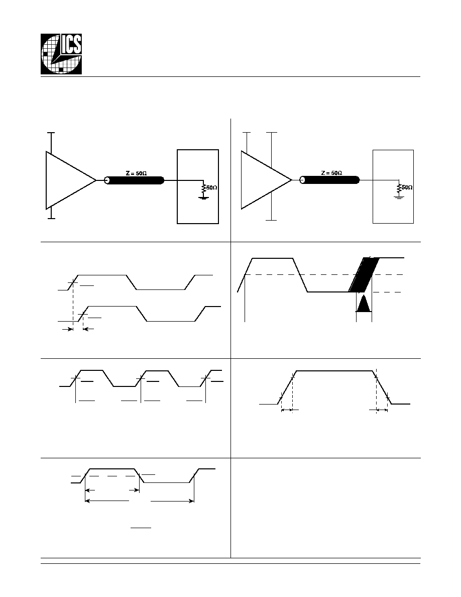
- Parallel & Serial Load Operations Diagram
- Pin Descriptions
- Pin Characteristics
- Parallel & Serial Mode Function Table
- Programmable VCO Frequency Function Table
- Programmable Output Divider Function Table
- Output Enable & Clock Enable Function Table
- Absolute Maximum Ratings
- Power Supply DC Characteristics
- LVCMOS DC Characteristics
- Input Frequency Characteristics
- Crystal Characterisitics
- 3.3V AC Characteristics
- 3.3V/2.5V AC Characteristics
- Parameter Measurement Information
- 3.3V Core/3.3V Output Load AC Test Circuit Diagram
- 3.3V Core/2.5V Output Load AC Test Circuit Diagram
- Output Skew Diagram
- Period Jitter Diagram
- Cycle-to-Cycle Jitter Diagram
- Output Rise/Fall Time Diagram
- Output duty Cycle/Pulse Width/Period Diagram
- Application Information
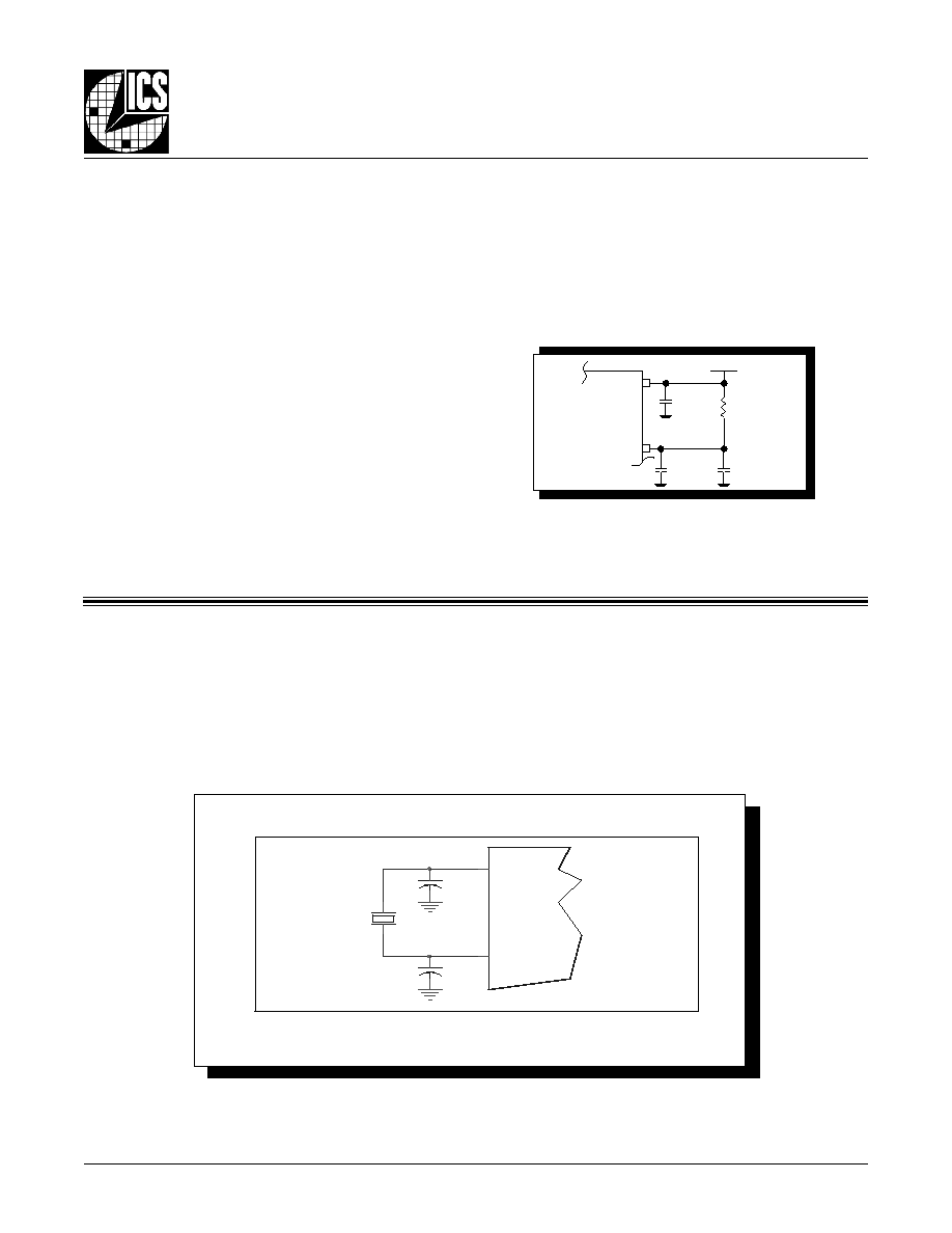
- Power Supply Filtering Techniques
- Crystal Input Interface
- Reliability Information
- Transistor Count
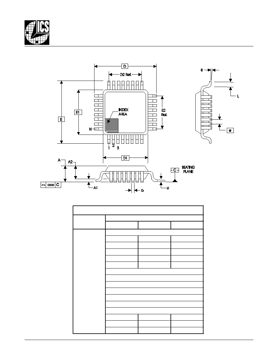
- Package Outline
- Package Dimensions
- Ordering Information

8402AYI
www.icst.com/products/hiperclocks.html
REV. A DECEMBER 23, 2004
1
Integrated
Circuit
Systems, Inc.
ICS8402I
350MH
Z
, C
RYSTAL
-
TO
-LVCMOS / LVTTL
F
REQUENCY
S
YNTHESIZER
G
ENERAL
D
ESCRIPTION
The ICS8402I is a general purpose, Crystal-to-
LVCMOS/LVTTL High Frequency Synthesizer and
a member of the HiPerClockS TM family of High
Performance Clock Solutions from ICS. The
ICS8402I has a selectable TEST_CLK or crystal
inputs. The VCO operates at a frequency range of 250MHz
to 700MHz. The VCO frequency is programmed in steps equal
to the value of the input reference or crystal frequency. The
VCO and output frequency can be programmed using the
serial or parallel interfaces to the configuration logic. The low
phase noise characteristics of the ICS8402I make it an ideal
clock source for Gigabit Ethernet and SONET applications.
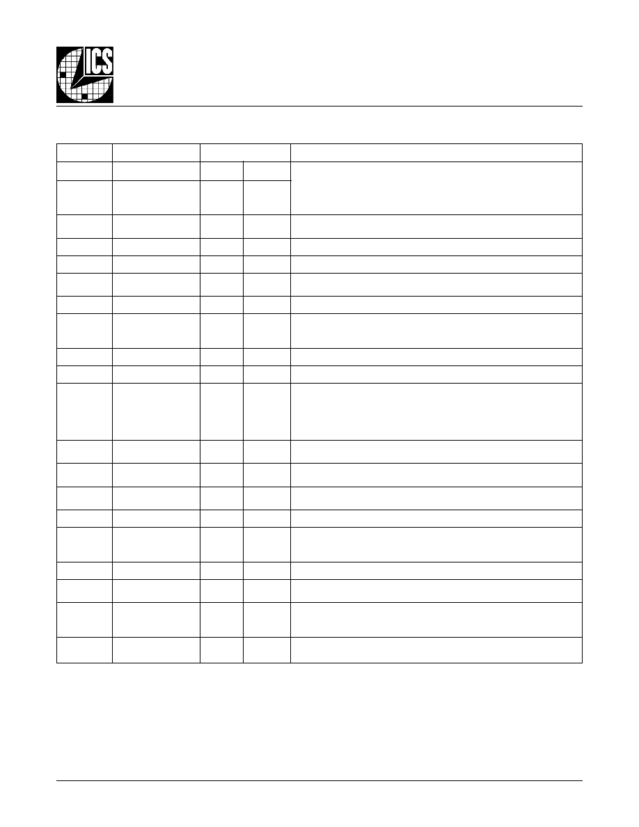
B
LOCK
D
IAGRAM
P
IN
A
SSIGNMENT
F
EATURES
∑ (2) LVCMOS/LVTTL outputs
∑ Selectable crystal oscillator interface
or LVCMOS/LVTTL TEST_CLK
∑ Output frequency range: 15.625MHz - 350MHz
∑ Crystal input frequency range: 12MHz to 40MHz
∑ VCO range: 250MHz to 700MHz
∑ Parallel or serial interface for programming counter
and output dividers
∑ RMS period jitter: 30ps (maximum)
∑ Cycle-to-cycle jitter: 100ps (maximum)
∑ Full 3.3V or mixed 3.3V core/2.5V output supply voltage
∑ -40∞C to 85∞C ambient operating temperature
∑ Lead-Free fully RoHS compliant
32 31 30 29 28 27 26 25
9 10 11 12 13 14 15 16
1
2
3
4
5
6
7
8
24
23
22
21
20
19
18
17
XTAL_OUT
TEST_CLK
XTAL_SEL
V
DDA
S_LOAD
S_DATA
S_CLOCK
MR
M5
M6
M7
M8
N0
N1
nc
GND
32-Lead LQFP
7mm x 7mm x 1.4mm package body
Y Package
Top View
ICS8402I
HiPerClockSTM
ICS
OSC
OE0
OE1
VCO_SEL
XTAL_SEL
TEST_CLK
XTAL_IN
XTAL_OUT
S_LOAD
S_DATA
S_CLOCK
nP_LOAD
M0:M8
N0:N1
VCO
PLL
Q0
Q1
TEST
CONFIGURATION
INTERFACE
LOGIC
˜ M
0
1
0
1
PHASE DETECTOR
˜2
˜4
˜8
˜16
MR
TEST
V
DD
OE1
OE0
V
DDO
Q1
Q0
GND
XT
AL_IN
nP_LO
A
D
VCO_SEL
M0
M1
M2
M3
M4

8402AYI
www.icst.com/products/hiperclocks.html
REV. A DECEMBER 23, 2004
2
Integrated
Circuit
Systems, Inc.
ICS8402I
350MH
Z
, C
RYSTAL
-
TO
-LVCMOS / LVTTL
F
REQUENCY
S
YNTHESIZER
put divider to a specific default state that will automatically
occur during power-up. The TEST output is LOW when op-
erating in the parallel input mode. The relationship between
the VCO frequency, the crystal frequency and the M divider
is defined as follows:
The M value and the required values of M0 through M8 are
shown in Table 3B, Programmable VCO Frequency Function
Table. Valid M values for which the PLL will achieve lock for a
25MHz reference are defined as 10
M 28. The frequency
out is defined as follows:
Serial operation occurs when nP_LOAD is HIGH and
S_LOAD is LOW. The shift register is loaded by sampling
the S_DATA bits with the rising edge of S_CLOCK. The con-
tents of the shift register are loaded into the M divider and N
output divider when S_LOAD transitions from LOW-to-HIGH.
The M divide and N output divide values are latched on the
HIGH-to-LOW transition of S_LOAD. If S_LOAD is held HIGH,
data at the S_DATA input is passed directly to the M divider
and N output divider on each rising edge of S_CLOCK. The
serial mode can be used to program the M and N bits and
test bits T1 and T0. The internal registers T0 and T1 deter-
mine the state of the TEST output as follows:
NOTE: The functional description that follows describes op-
eration using a 25MHz crystal. Valid PLL loop divider values
for different crystal or input frequencies are defined in the
Input Frequency Characteristics, Table 5, NOTE 1.
The ICS8402I features a fully integrated PLL and therefore
requires no external components for setting the loop band-
width. A fundamental crystal is used as the input to the on-
chip oscillator. The output of the oscillator is fed into the phase
detector. A 25MHz crystal provides a 25MHz phase detector
reference frequency. The VCO of the PLL operates over a
range of 250MHz to 700MHz. The output of the M divider is
also applied to the phase detector.
The phase detector and the M divider force the VCO output
frequency to be M times the reference frequency by adjusting
the VCO control voltage. Note that for some values of M (either
too high or too low), the PLL will not achieve lock. The output of
the VCO is scaled by a divider prior to being sent to each of
the LVCMOS output buffers. The divider provides a 50% out-
put duty cycle.
The programmable features of the ICS8402I support two in-
put modes to program the M divider and N output divider.
The two input operational modes are parallel and serial.
Fig-
ure 1 shows the timing diagram for each mode. In parallel
mode, the nP_LOAD input is initially LOW. The data on in-
puts M0 through M8 and N0 and N1 is passed directly to the
M divider and N output divider. On the LOW-to-HIGH transi-
tion of the nP_LOAD input, the data is latched and the M
divider remains loaded until the next LOW transition on
nP_LOAD or until a serial event occurs. As a result, the M
and N bits can be hardwired to set the M divider and N out-
F
UNCTIONAL
D
ESCRIPTION
fVCO = fxtal x M
T1
T0
TEST Output
0
0
LOW
0
1
Shift Register Output
1
0
Output of M divider
1
1
CMOS Fout
F
IGURE
1. P
ARALLEL
& S
ERIAL
L
OAD
O
PERATIONS
*NOTE: The NULL timing slot must be observed.
Time
S
ERIAL
L
OADING
P
ARALLEL
L
OADING
M, N
t
S
t
H
t
S
t
H
t
S
T 1
T0
*NULL
N1
N0
M8
M7
M6
M5
M4
M3
M2
M1
M 0
FOUT = fVCO = fxtal x M
N
N
S_CLOCK
S_DATA
S_LOAD
nP_LOAD
M0:M8, N0:N1
nP_LOAD
8402AYI
www.icst.com/products/hiperclocks.html
REV. A DECEMBER 23, 2004
3
Integrated
Circuit
Systems, Inc.
ICS8402I
350MH
Z
, C
RYSTAL
-
TO
-LVCMOS / LVTTL
F
REQUENCY
S
YNTHESIZER
T
ABLE
1. P
IN
D
ESCRIPTIONS
r
e
b
m
u
N
e
m
a
N
e
p
y
T
n
o
i
t
p
i
r
c
s
e
D
1
5
M
t
u
p
n
I
p
u
ll
u
P
n
o
i
t
i
s
n
a
r
t
H
G
I
H
-
o
t
-
W
O
L
n
o
d
e
h
c
t
a
l
a
t
a
D
.
s
t
u
p
n
i
r
e
d
i
v
i
d
M
.
s
l
e
v
e
l
e
c
a
f
r
e
t
n
i
L
T
T
V
L
/
S
O
M
C
V
L
.
t
u
p
n
i
D
A
O
L
_
P
n
f
o
,
4
,
3
,
2
,
9
2
,
8
2
2
3
,
1
3
,
0
3
,
8
M
,
7
M
,
6
M
,
1
M
,
0
M
4
M
,
3
M
,
2
M
t
u
p
n
I
n
w
o
d
ll
u
P
6
,
5
1
N
,
0
N
t
u
p
n
I
n
w
o
d
ll
u
P
,
C
3
e
l
b
a
T
n
i
d
e
n
i
f
e
d
s
a
e
u
l
a
v
r
e
d
i
v
i
d
t
u
p
t
u
o
s
e
n
i
m
r
e
t
e
D
.
s
l
e
v
e
l
e
c
a
f
r
e
t
n
i
L
T
T
V
L
/
S
O
M
C
V
L
.
e
l
b
a
T
n
o
i
t
c
n
u
F
7
c
n
d
e
s
u
n
U
.
t
c
e
n
n
o
c
o
N
6
1
,
8
D
N
G
r
e
w
o
P
.
d
n
u
o
r
g
y
l
p
p
u
s
r
e
w
o
P
9
T
S
E
T
t
u
p
t
u
O
t
u
p
t
u
O
.
n
o
i
t
a
r
e
p
o
f
o
e
d
o
m
l
a
i
r
e
s
e
h
t
n
i
E
V
I
T
C
A
s
i
h
c
i
h
w
t
u
p
t
u
o
t
s
e
T
.
s
l
e
v
e
l
e
c
a
f
r
e
t
n
i
L
T
T
V
L
/
S
O
M
C
V
L
.
e
d
o
m
l
e
ll
a
r
a
p
n
i
W
O
L
n
e
v
i
r
d
0
1
V
D
D
r
e
w
o
P
.
n
i
p
y
l
p
p
u
s
e
r
o
C
2
1
,
1
1
0
E
O
,
1
E
O
t
u
p
n
I
p
u
ll
u
P
.
)
t
l
u
a
f
e
d
(
d
e
l
b
a
n
e
e
r
a
s
t
u
p
t
u
o
e
h
t
,
H
G
I
H
c
i
g
o
l
n
e
h
W
.
e
l
b
a
n
e
t
u
p
t
u
O
,
D
3
e
l
b
a
T
e
e
S
.
e
t
a
t
S
-
i
r
T
n
i
e
r
a
s
t
u
p
t
u
o
e
h
t
,
W
O
L
c
i
g
o
l
n
e
h
W
.
s
l
e
v
e
l
e
c
a
f
r
e
t
n
i
L
T
T
V
L
/
S
O
M
C
V
L
.
e
l
b
a
T
n
o
i
t
c
n
u
F
E
O
3
1
V
O
D
D
r
e
w
o
P
.
n
i
p
y
l
p
p
u
s
t
u
p
t
u
O
5
1
,
4
1
0
Q
,
1
Q
t
u
p
t
u
O
.
s
l
e
v
e
l
e
c
a
f
r
e
t
n
i
L
T
T
V
L
/
S
O
M
C
V
L
.
s
t
u
p
t
u
o
k
c
o
l
C
7
1
R
M
t
u
p
n
I
n
w
o
d
ll
u
P
s
r
e
d
i
v
i
d
l
a
n
r
e
t
n
i
e
h
t
,
H
G
I
H
c
i
g
o
l
n
e
h
W
.
t
e
s
e
R
r
e
t
s
a
M
h
g
i
H
e
v
i
t
c
A
e
h
t
,
W
O
L
c
i
g
o
l
n
e
h
W
.
w
o
l
o
g
o
t
s
t
u
p
t
u
o
e
h
t
g
n
i
s
u
a
c
t
e
s
e
r
e
r
a
R
M
f
o
n
o
i
t
r
e
s
s
A
.
d
e
l
b
a
n
e
e
r
a
s
t
u
p
t
u
o
e
h
t
d
n
a
s
r
e
d
i
v
i
d
l
a
n
r
e
t
n
i
.
s
e
u
l
a
v
T
d
n
a
,
N
,
M
d
e
d
a
o
l
t
c
e
f
f
e
t
o
n
s
e
o
d
.
s
l
e
v
e
l
e
c
a
f
r
e
t
n
i
L
T
T
V
L
/
S
O
M
C
V
L
8
1
K
C
O
L
C
_
S
t
u
p
n
I
n
w
o
d
ll
u
P
r
e
t
s
i
g
e
r
t
f
i
h
s
e
h
t
o
t
n
i
t
u
p
n
i
A
T
A
D
_
S
t
a
t
n
e
s
e
r
p
a
t
a
d
l
a
i
r
e
s
n
i
s
k
c
o
l
C
.
s
l
e
v
e
l
e
c
a
f
r
e
t
n
i
L
T
T
V
L
/
S
O
M
C
V
L
.
K
C
O
L
C
_
S
f
o
e
g
d
e
g
n
i
s
i
r
e
h
t
n
o
9
1
A
T
A
D
_
S
t
u
p
n
I
n
w
o
d
ll
u
P
f
o
e
g
d
e
g
n
i
s
i
r
e
h
t
n
o
d
e
l
p
m
a
s
a
t
a
D
.
t
u
p
n
i
l
a
i
r
e
s
r
e
t
s
i
g
e
r
t
f
i
h
S
.
s
l
e
v
e
l
e
c
a
f
r
e
t
n
i
L
T
T
V
L
/
S
O
M
C
V
L
.
K
C
O
L
C
_
S
0
2
D
A
O
L
_
S
t
u
p
n
I
n
w
o
d
ll
u
P
.
s
r
e
d
i
v
i
d
e
h
t
o
t
n
i
r
e
t
s
i
g
e
r
t
f
i
h
s
m
o
r
f
a
t
a
d
f
o
n
o
i
t
i
s
n
a
r
t
s
l
o
r
t
n
o
C
.
s
l
e
v
e
l
e
c
a
f
r
e
t
n
i
L
T
T
V
L
/
S
O
M
C
V
L
1
2
V
A
D
D
r
e
w
o
P
.
n
i
p
y
l
p
p
u
s
g
o
l
a
n
A
2
2
L
E
S
_
L
A
T
X
t
u
p
n
I
p
u
ll
u
P
.
e
c
r
u
o
s
e
c
n
e
r
e
f
e
r
L
L
P
e
h
t
s
a
s
t
u
p
n
i
t
s
e
t
r
o
l
a
t
s
y
r
c
n
e
e
w
t
e
b
s
t
c
e
l
e
S
.
W
O
L
n
e
h
w
K
L
C
_
T
S
E
T
s
t
c
e
l
e
S
.
H
G
I
H
n
e
h
w
s
t
u
p
n
i
L
A
T
X
s
t
c
e
l
e
S
s
l
e
v
e
l
e
c
a
f
r
e
t
n
i
L
T
T
V
L
/
S
O
M
C
V
L
3
2
K
L
C
_
T
S
E
T
t
u
p
n
I
n
w
o
d
ll
u
P
.
s
l
e
v
e
l
e
c
a
f
r
e
t
n
i
L
T
T
V
L
/
S
O
M
C
V
L
.
t
u
p
n
i
k
c
o
l
c
t
s
e
T
5
2
,
4
2
,
T
U
O
_
L
A
T
X
N
I
_
L
A
T
X
t
u
p
n
I
.
t
u
p
n
i
e
h
t
s
i
N
I
_
L
A
T
X
.
e
c
a
f
r
e
t
n
i
r
o
t
a
ll
i
c
s
o
l
a
t
s
y
r
C
.
t
u
p
t
u
o
e
h
t
s
i
T
U
O
_
L
A
T
X
6
2
D
A
O
L
_
P
n
t
u
p
n
I
n
w
o
d
ll
u
P
s
i
0
M
:
8
M
t
a
t
n
e
s
e
r
p
a
t
a
d
n
e
h
w
s
e
n
i
m
r
e
t
e
D
.
t
u
p
n
i
d
a
o
l
l
e
ll
a
r
a
P
e
h
t
s
t
e
s
0
N
:
1
N
t
a
t
n
e
s
e
r
p
a
t
a
d
n
e
h
w
d
n
a
,
r
e
d
i
v
i
d
M
o
t
n
i
d
e
d
a
o
l
.
s
l
e
v
e
l
e
c
a
f
r
e
t
n
i
L
T
T
V
L
/
S
O
M
C
V
L
.
e
u
l
a
v
r
e
d
i
v
i
d
t
u
p
t
u
o
N
7
2
L
E
S
_
O
C
V
t
u
p
n
I
p
u
ll
u
P
.
e
d
o
m
s
s
a
p
y
b
r
o
L
L
P
n
i
s
i
r
e
z
i
s
e
h
t
n
y
s
r
e
h
t
e
h
w
s
e
n
i
m
r
e
t
e
D
.
s
l
e
v
e
l
e
c
a
f
r
e
t
n
i
L
T
T
V
L
/
S
O
M
C
V
L
:
E
T
O
N
p
u
ll
u
P
d
n
a
n
w
o
d
ll
u
P
.
s
e
u
l
a
v
l
a
c
i
p
y
t
r
o
f
,
s
c
i
t
s
i
r
e
t
c
a
r
a
h
C
n
i
P
,
2
e
l
b
a
T
e
e
S
.
s
r
o
t
s
i
s
e
r
t
u
p
n
i
l
a
n
r
e
t
n
i
o
t
r
e
f
e
r
8402AYI
www.icst.com/products/hiperclocks.html
REV. A DECEMBER 23, 2004
4
Integrated
Circuit
Systems, Inc.
ICS8402I
350MH
Z
, C
RYSTAL
-
TO
-LVCMOS / LVTTL
F
REQUENCY
S
YNTHESIZER
T
ABLE
3A. P
ARALLEL
AND
S
ERIAL
M
ODE
F
UNCTION
T
ABLE
s
t
u
p
n
I
s
n
o
i
t
i
d
n
o
C
R
M
D
A
O
L
_
P
n
M
N
D
A
O
L
_
S
K
C
O
L
C
_
S
A
T
A
D
_
S
H
X
X
X
X
X
X
.
W
O
L
s
t
u
p
t
u
o
s
e
c
r
o
F
.
t
e
s
e
R
L
L
a
t
a
D
a
t
a
D
X
X
X
M
e
h
t
o
t
y
l
t
c
e
r
i
d
d
e
s
s
a
p
s
t
u
p
n
i
N
d
n
a
M
n
o
a
t
a
D
.
W
O
L
d
e
c
r
o
f
t
u
p
t
u
o
T
S
E
T
.
r
e
d
i
v
i
d
t
u
p
t
u
o
N
d
n
a
r
e
d
i
v
i
d
L
a
t
a
D
a
t
a
D
L
X
X
d
e
d
a
o
l
s
n
i
a
m
e
r
d
n
a
s
r
e
t
s
i
g
e
r
t
u
p
n
i
o
t
n
i
d
e
h
c
t
a
l
s
i
a
t
a
D
.
s
r
u
c
c
o
t
n
e
v
e
l
a
i
r
e
s
a
li
t
n
u
r
o
n
o
i
t
i
s
n
a
r
t
W
O
L
t
x
e
n
li
t
n
u
L
H
X
X
L
a
t
a
D
n
o
a
t
a
d
h
t
i
w
d
e
d
a
o
l
s
i
r
e
t
s
i
g
e
r
t
f
i
h
S
.
e
d
o
m
t
u
p
n
i
l
a
i
r
e
S
.
K
C
O
L
C
_
S
f
o
e
g
d
e
g
n
i
s
i
r
h
c
a
e
n
o
A
T
A
D
_
S
L
H
X
X
L
a
t
a
D
e
h
t
o
t
d
e
s
s
a
p
e
r
a
r
e
t
s
i
g
e
r
t
f
i
h
s
e
h
t
f
o
s
t
n
e
t
n
o
C
.
r
e
d
i
v
i
d
t
u
p
t
u
o
N
d
n
a
r
e
d
i
v
i
d
M
L
H
X
X
L
a
t
a
D
.
d
e
h
c
t
a
l
e
r
a
s
e
u
l
a
v
r
e
d
i
v
i
d
t
u
p
t
u
o
N
d
n
a
r
e
d
i
v
i
d
M
L
H
X
X
L
X
X
.
s
r
e
t
s
i
g
e
r
t
f
i
h
s
t
c
e
f
f
a
t
o
n
o
d
t
u
p
n
i
l
a
i
r
e
s
r
o
l
e
ll
a
r
a
P
L
H
X
X
H
a
t
a
D
.
d
e
k
c
o
l
c
s
i
t
i
s
a
r
e
d
i
v
i
d
M
o
t
y
l
t
c
e
r
i
d
d
e
s
s
a
p
A
T
A
D
_
S
W
O
L
=
L
:
E
T
O
N
H
G
I
H
=
H
e
r
a
c
t
'
n
o
D
=
X
n
o
i
t
i
s
n
a
r
t
e
g
d
e
g
n
i
s
i
R
=
n
o
i
t
i
s
n
a
r
t
e
g
d
e
g
n
il
l
a
F
=
T
ABLE
2. P
IN
C
HARACTERISTICS
l
o
b
m
y
S
r
e
t
e
m
a
r
a
P
s
n
o
i
t
i
d
n
o
C
t
s
e
T
m
u
m
i
n
i
M
l
a
c
i
p
y
T
m
u
m
i
x
a
M
s
t
i
n
U
C
N
I
e
c
n
a
t
i
c
a
p
a
C
t
u
p
n
I
4
F
p
C
D
P
e
c
n
a
t
i
c
a
p
a
C
n
o
i
t
a
p
i
s
s
i
D
r
e
w
o
P
)
t
u
p
t
u
o
r
e
p
(
V
D
D
V
,
A
D
D
V
,
O
D
D
V
5
6
4
.
3
=
3
1
F
p
V
D
D
V
,
A
D
D
V
,
V
5
6
4
.
3
=
O
D
D
V
5
2
6
.
2
=
1
1
F
p
R
P
U
L
L
U
P
r
o
t
s
i
s
e
R
p
u
ll
u
P
t
u
p
n
I
1
5
K
R
N
W
O
D
L
L
U
P
r
o
t
s
i
s
e
R
n
w
o
d
ll
u
P
t
u
p
n
I
1
5
K
R
T
U
O
e
c
n
a
d
e
p
m
I
t
u
p
t
u
O
V
O
D
D
V
5
6
4
.
3
=
5
7
2
1
V
O
D
D
V
5
2
6
.
2
=
7
8402AYI
www.icst.com/products/hiperclocks.html
REV. A DECEMBER 23, 2004
5
Integrated
Circuit
Systems, Inc.
ICS8402I
350MH
Z
, C
RYSTAL
-
TO
-LVCMOS / LVTTL
F
REQUENCY
S
YNTHESIZER
T
ABLE
3B. P
ROGRAMMABLE
VCO F
REQUENCY
F
UNCTION
T
ABLE
T
ABLE
3C. P
ROGRAMMABLE
O
UTPUT
D
IVIDER
F
UNCTION
T
ABLE
s
t
u
p
n
I
e
u
l
a
V
r
e
d
i
v
i
D
N
y
c
n
e
u
q
e
r
F
t
u
p
t
u
O
)
z
H
M
(
1
N
0
N
m
u
m
i
n
i
M
m
u
m
i
x
a
M
0
0
2
5
2
1
0
5
3
0
1
4
5
.
2
6
5
7
1
1
0
8
5
2
.
1
3
5
.
7
8
1
1
6
1
5
2
6
.
5
1
5
7
.
3
4
y
c
n
e
u
q
e
r
F
O
C
V
)
z
H
M
(
e
d
i
v
i
D
M
6
5
2
8
2
1
4
6
2
3
6
1
8
4
2
1
8
M
7
M
6
M
5
M
4
M
3
M
2
M
1
M
0
M
0
5
2
0
1
0
0
0
0
0
1
0
1
0
5
7
2
1
1
0
0
0
0
0
1
0
1
1
∑
∑
∑
∑
∑
∑
∑
∑
∑
∑
∑
∑
∑
∑
∑
∑
∑
∑
∑
∑
∑
∑
0
5
6
6
2
0
0
0
0
1
1
0
1
0
5
7
6
7
2
0
0
0
0
1
1
0
1
1
0
0
7
8
2
0
0
0
0
1
1
1
0
0
y
c
n
e
u
q
e
r
f
t
u
p
n
i
K
L
C
_
T
S
E
T
r
o
l
a
t
s
y
r
c
o
t
d
n
o
p
s
e
r
r
o
c
s
e
i
c
n
e
u
q
e
r
f
g
n
i
t
l
u
s
e
r
e
h
t
d
n
a
s
e
u
l
a
v
e
d
i
v
i
d
M
e
s
e
h
T
:
1
E
T
O
N
.
z
H
M
5
2
f
o
T
ABLE
3D. O
UTPUT
E
NABLE
& C
LOCK
E
NABLE
F
UNCTION
T
ABLE
s
t
u
p
n
I
l
o
r
t
n
o
C
t
u
p
t
u
O
0
E
O
1
E
O
0
Q
1
Q
0
0
Z
-
i
H
Z
-
i
H
0
1
Z
-
i
H
d
e
l
b
a
n
E
1
0
d
e
l
b
a
n
E
Z
-
i
H
1
1
d
e
l
b
a
n
E
d
e
l
b
a
n
E

8402AYI
www.icst.com/products/hiperclocks.html
REV. A DECEMBER 23, 2004
6
Integrated
Circuit
Systems, Inc.
ICS8402I
350MH
Z
, C
RYSTAL
-
TO
-LVCMOS / LVTTL
F
REQUENCY
S
YNTHESIZER
T
ABLE
4A. P
OWER
S
UPPLY
DC C
HARACTERISTICS
,
V
DD
= V
DDA
= 3.3V±5%, V
DDO
= 3.3V±5%
OR
2.5V±5%, T
A
= -40∞C
TO
85∞C
T
ABLE
4B. LVCMOS / LVTTL DC C
HARACTERISTICS
,
V
DD
= V
DDA
= 3.3V±5%, V
DDO
= 3.3V±5%
OR
2.5V±5%, T
A
= -40∞C
TO
85∞C
l
o
b
m
y
S
r
e
t
e
m
a
r
a
P
s
n
o
i
t
i
d
n
o
C
t
s
e
T
m
u
m
i
n
i
M
l
a
c
i
p
y
T
m
u
m
i
x
a
M
s
t
i
n
U
V
H
I
t
u
p
n
I
e
g
a
t
l
o
V
h
g
i
H
,
R
M
,
L
E
S
_
L
A
T
X
,
L
E
S
_
O
C
V
,
A
T
A
D
_
S
,
D
A
O
L
_
P
n
,
D
A
O
L
_
S
,
1
E
O
,
0
E
O
,
K
C
O
L
C
_
S
8
M
:
0
M
,
1
N
:
0
N
2
V
D
D
3
.
0
+
V
K
L
C
_
T
S
E
T
2
V
D
D
3
.
0
+
V
V
L
I
t
u
p
n
I
e
g
a
t
l
o
V
w
o
L
,
R
M
,
L
E
S
_
L
A
T
X
,
L
E
S
_
O
C
V
,
A
T
A
D
_
S
,
D
A
O
L
_
P
n
,
D
A
O
L
_
S
,
1
E
O
,
0
E
O
,
K
C
O
L
C
_
S
8
M
:
0
M
,
1
N
:
0
N
3
.
0
-
8
.
0
V
K
L
C
_
T
S
E
T
3
.
0
-
3
.
1
V
I
H
I
t
u
p
n
I
t
n
e
r
r
u
C
h
g
i
H
,
R
M
,
1
N
,
0
N
,
8
M
-
6
M
,
4
M
-
0
M
,
K
L
C
_
T
S
E
T
,
K
C
O
L
C
_
S
D
A
O
L
_
P
n
,
D
A
O
L
_
S
,
A
T
A
D
_
S
V
D
D
V
=
N
I
V
5
6
4
.
3
=
0
5
1
A
µ
,
1
E
O
,
0
E
O
,
5
M
L
E
S
_
O
C
V
,
L
E
S
_
L
A
T
X
V
D
D
V
=
N
I
V
5
6
4
.
3
=
5
A
µ
I
L
I
t
u
p
n
I
t
n
e
r
r
u
C
w
o
L
,
R
M
,
1
N
,
0
N
,
8
M
-
6
M
,
4
M
-
0
M
,
K
L
C
_
T
S
E
T
,
K
C
O
L
C
_
S
D
A
O
L
_
P
n
,
D
A
O
L
_
S
,
A
T
A
D
_
S
V
D
D
,
V
5
6
4
.
3
=
V
N
I
V
0
=
5
-
A
µ
,
1
E
O
,
0
E
O
,
5
M
L
E
S
_
O
C
V
,
L
E
S
_
L
A
T
X
V
D
D
,
V
5
6
4
.
3
=
V
N
I
V
0
=
0
5
1
-
A
µ
V
H
O
1
E
T
O
N
;
e
g
a
t
l
o
V
h
g
i
H
t
u
p
t
u
O
V
O
D
D
V
5
6
4
.
3
=
6
.
2
V
V
O
D
D
V
5
2
6
.
2
=
8
.
1
V
V
L
O
1
E
T
O
N
;
e
g
a
t
l
o
V
w
o
L
t
u
p
t
u
O
5
.
0
V
NOTE 1: Outputs terminated with 50
to V
DDO
/2.
l
o
b
m
y
S
r
e
t
e
m
a
r
a
P
s
n
o
i
t
i
d
n
o
C
t
s
e
T
m
u
m
i
n
i
M
l
a
c
i
p
y
T
m
u
m
i
x
a
M
s
t
i
n
U
V
D
D
e
g
a
t
l
o
V
y
l
p
p
u
S
e
r
o
C
5
3
1
.
3
3
.
3
5
6
4
.
3
V
V
A
D
D
e
g
a
t
l
o
V
y
l
p
p
u
S
g
o
l
a
n
A
5
3
1
.
3
3
.
3
5
6
4
.
3
V
V
O
D
D
e
g
a
t
l
o
V
y
l
p
p
u
S
t
u
p
t
u
O
5
3
1
.
3
3
.
3
5
6
4
.
3
V
5
7
3
.
2
5
.
2
5
2
6
.
2
V
I
D
D
t
n
e
r
r
u
C
y
l
p
p
u
S
r
e
w
o
P
5
2
1
A
m
I
A
D
D
t
n
e
r
r
u
C
y
l
p
p
u
S
g
o
l
a
n
A
8
1
A
m
I
O
D
D
t
n
e
r
r
u
C
y
l
p
p
u
S
t
u
p
t
u
O
0
1
A
m
A
BSOLUTE
M
AXIMUM
R
ATINGS
Supply Voltage, V
DD
4.6V
Inputs, V
I
-0.5V to V
DD
+ 0.5 V
Outputs, V
O
-0.5V to V
DDO
+ 0.5V
Package Thermal Impedance,
JA
47.9∞C/W (0 lfpm)
Storage Temperature, T
STG
-65∞C to 150∞C
NOTE: Stresses beyond those listed under Absolute
Maximum Ratings may cause permanent damage to the
device. These ratings are stress specifications only. Functional
operation of product at these conditions or any conditions
beyond those listed in the
DC Characteristics or AC Charac-
teristics is not implied. Exposure to absolute maximum rating
conditions for extended periods may affect product reliability.
8402AYI
www.icst.com/products/hiperclocks.html
REV. A DECEMBER 23, 2004
7
Integrated
Circuit
Systems, Inc.
ICS8402I
350MH
Z
, C
RYSTAL
-
TO
-LVCMOS / LVTTL
F
REQUENCY
S
YNTHESIZER
T
ABLE
5. I
NPUT
F
REQUENCY
C
HARACTERISTICS
,
V
DD
= V
DDA
= V
DDO
= 3.3V±5%, T
A
= -40∞C
TO
85∞C
l
o
b
m
y
S
r
e
t
e
m
a
r
a
P
s
n
o
i
t
i
d
n
o
C
t
s
e
T
m
u
m
i
n
i
M
l
a
c
i
p
y
T
m
u
m
i
x
a
M
s
t
i
n
U
f
N
I
t
u
p
n
I
y
c
n
e
u
q
e
r
F
1
E
T
O
N
;
K
L
C
_
T
S
E
T
2
1
0
4
z
H
M
1
E
T
O
N
T
U
O
_
L
A
T
X
N
I
_
L
A
T
X
2
1
0
4
z
H
M
K
C
O
L
C
_
S
0
5
z
H
M
n
i
h
t
i
w
e
t
a
r
e
p
o
o
t
O
C
V
e
h
t
r
o
f
t
e
s
e
b
t
s
u
m
e
u
l
a
v
M
e
h
t
,
e
g
n
a
r
y
c
n
e
u
q
e
r
f
K
L
C
_
T
S
E
T
d
n
a
l
a
t
s
y
r
c
t
u
p
n
i
e
h
t
r
o
F
:
1
E
T
O
N
1
2
e
r
a
M
f
o
s
e
u
l
a
v
d
il
a
v
,
z
H
M
2
1
f
o
y
c
n
e
u
q
e
r
f
t
u
p
n
i
m
u
m
i
n
i
m
e
h
t
g
n
i
s
U
.
e
g
n
a
r
z
H
M
0
0
7
o
t
z
H
M
0
5
2
e
h
t
M
.
8
5
7
e
r
a
M
f
o
s
e
u
l
a
v
d
il
a
v
,
z
H
M
0
4
f
o
y
c
n
e
u
q
e
r
f
m
u
m
i
x
a
m
e
h
t
g
n
i
s
U
M
.
7
1
T
ABLE
6. C
RYSTAL
C
HARACTERISTICS
r
e
t
e
m
a
r
a
P
s
n
o
i
t
i
d
n
o
C
t
s
e
T
m
u
m
i
n
i
M
l
a
c
i
p
y
T
m
u
m
i
x
a
M
s
t
i
n
U
n
o
i
t
a
ll
i
c
s
O
f
o
e
d
o
M
l
a
t
n
e
m
a
d
n
u
F
y
c
n
e
u
q
e
r
F
2
1
0
4
z
H
M
)
R
S
E
(
e
c
n
a
t
s
i
s
e
R
s
e
i
r
e
S
t
n
e
l
a
v
i
u
q
E
0
5
C
(
e
c
n
a
t
i
c
a
p
a
C
t
n
u
h
S
O
)
7
F
p
l
o
b
m
y
S
r
e
t
e
m
a
r
a
P
s
n
o
i
t
i
d
n
o
C
t
s
e
T
m
u
m
i
n
i
M
l
a
c
i
p
y
T
m
u
m
i
x
a
M
s
t
i
n
U
F
T
U
O
y
c
n
e
u
q
e
r
F
t
u
p
t
u
O
5
2
6
.
5
1
0
5
3
z
H
M
t
)
c
c
(
t
ij
3
,
1
E
T
O
N
;
r
e
t
t
i
J
e
l
c
y
C
-
o
t
-
e
l
c
y
C
0
4
0
0
1
s
p
t
)
r
e
p
(
t
ij
1
E
T
O
N
;
S
M
R
,
r
e
t
t
i
J
d
o
i
r
e
P
8
0
3
s
p
t
)
o
(
k
s
3
,
2
E
T
O
N
;
w
e
k
S
t
u
p
t
u
O
0
8
s
p
t
R
t
/
F
e
m
i
T
ll
a
F
/
e
s
i
R
t
u
p
t
u
O
%
0
8
o
t
%
0
2
5
2
.
0
1
.
1
s
n
t
S
e
m
i
T
p
u
t
e
S
D
A
O
L
_
P
n
o
t
N
,
M
5
s
n
K
C
O
L
C
_
S
o
t
A
T
A
D
_
S
5
s
n
D
A
O
L
_
S
o
t
K
C
O
L
C
_
S
5
s
n
t
H
e
m
i
T
d
l
o
H
D
A
O
L
_
P
n
o
t
N
,
M
5
s
n
K
C
O
L
C
_
S
o
t
A
T
A
D
_
S
5
s
n
D
A
O
L
_
S
o
t
K
C
O
L
C
_
S
5
s
n
c
d
o
e
l
c
y
C
y
t
u
D
t
u
p
t
u
O
z
H
M
0
0
3
0
4
0
6
%
t
K
C
O
L
e
m
i
T
k
c
o
L
L
L
P
1
s
m
.
n
o
i
t
c
e
s
n
o
i
t
a
m
r
o
f
n
I
t
n
e
m
e
r
u
s
a
e
M
r
e
t
e
m
a
r
a
P
e
e
S
.
s
t
u
p
n
i
L
A
T
X
g
n
i
s
u
e
c
n
a
m
r
o
f
r
e
p
r
e
t
t
i
J
:
1
E
T
O
N
V
t
a
d
e
r
u
s
a
e
M
.
s
n
o
i
t
i
d
n
o
c
d
a
o
l
l
a
u
q
e
h
t
i
w
d
n
a
e
g
a
t
l
o
v
y
l
p
p
u
s
e
m
a
s
e
h
t
t
a
s
t
u
p
t
u
o
n
e
e
w
t
e
b
w
e
k
s
s
a
d
e
n
i
f
e
D
:
2
E
T
O
N
O
D
D
.
2
/
.
5
6
d
r
a
d
n
a
t
S
C
E
D
E
J
h
t
i
w
e
c
n
a
d
r
o
c
c
a
n
i
d
e
n
i
f
e
d
s
i
r
e
t
e
m
a
r
a
p
s
i
h
T
:
3
E
T
O
N
T
ABLE
7A. AC C
HARACTERISTICS
,
V
DD
= V
DDA
= V
DDO
= 3.3V±5%, T
A
= -40∞C
TO
85∞C
8402AYI
www.icst.com/products/hiperclocks.html
REV. A DECEMBER 23, 2004
8
Integrated
Circuit
Systems, Inc.
ICS8402I
350MH
Z
, C
RYSTAL
-
TO
-LVCMOS / LVTTL
F
REQUENCY
S
YNTHESIZER
l
o
b
m
y
S
r
e
t
e
m
a
r
a
P
s
n
o
i
t
i
d
n
o
C
t
s
e
T
m
u
m
i
n
i
M
l
a
c
i
p
y
T
m
u
m
i
x
a
M
s
t
i
n
U
F
T
U
O
y
c
n
e
u
q
e
r
F
t
u
p
t
u
O
5
2
6
.
5
1
0
5
3
z
H
M
t
)
c
c
(
t
ij
3
,
1
E
T
O
N
;
r
e
t
t
i
J
e
l
c
y
C
-
o
t
-
e
l
c
y
C
0
4
0
0
1
s
p
t
)
r
e
p
(
t
ij
1
E
T
O
N
;
S
M
R
,
r
e
t
t
i
J
d
o
i
r
e
P
0
3
s
p
t
)
o
(
k
s
3
,
2
E
T
O
N
;
w
e
k
S
t
u
p
t
u
O
0
6
s
p
t
R
t
/
F
e
m
i
T
ll
a
F
/
e
s
i
R
t
u
p
t
u
O
%
0
8
o
t
%
0
2
5
2
.
0
0
.
1
s
n
t
S
e
m
i
T
p
u
t
e
S
D
A
O
L
_
P
n
o
t
N
,
M
5
s
n
K
C
O
L
C
_
S
o
t
A
T
A
D
_
S
5
s
n
D
A
O
L
_
S
o
t
K
C
O
L
C
_
S
5
s
n
t
H
e
m
i
T
d
l
o
H
D
A
O
L
_
P
n
o
t
N
,
M
5
s
n
K
C
O
L
C
_
S
o
t
A
T
A
D
_
S
5
s
n
D
A
O
L
_
S
o
t
K
C
O
L
C
_
S
5
s
n
c
d
o
e
l
c
y
C
y
t
u
D
t
u
p
t
u
O
z
H
M
0
0
3
0
4
0
6
%
t
K
C
O
L
e
m
i
T
k
c
o
L
L
L
P
1
s
m
.
n
o
i
t
c
e
s
n
o
i
t
a
m
r
o
f
n
I
t
n
e
m
e
r
u
s
a
e
M
r
e
t
e
m
a
r
a
P
e
e
S
.
s
t
u
p
n
i
L
A
T
X
g
n
i
s
u
e
c
n
a
m
r
o
f
r
e
p
r
e
t
t
i
J
:
1
E
T
O
N
V
t
a
d
e
r
u
s
a
e
M
.
s
n
o
i
t
i
d
n
o
c
d
a
o
l
l
a
u
q
e
h
t
i
w
d
n
a
e
g
a
t
l
o
v
y
l
p
p
u
s
e
m
a
s
e
h
t
t
a
s
t
u
p
t
u
o
n
e
e
w
t
e
b
w
e
k
s
s
a
d
e
n
i
f
e
D
:
2
E
T
O
N
O
D
D
.
2
/
.
5
6
d
r
a
d
n
a
t
S
C
E
D
E
J
h
t
i
w
e
c
n
a
d
r
o
c
c
a
n
i
d
e
n
i
f
e
d
s
i
r
e
t
e
m
a
r
a
p
s
i
h
T
:
3
E
T
O
N
T
ABLE
7B. AC C
HARACTERISTICS
,
V
DD
= V
DDA
= 3.3V±5%, V
DDO
= 2.5V±5%, T
A
= -40∞C
TO
85∞C
8402AYI
www.icst.com/products/hiperclocks.html
REV. A DECEMBER 23, 2004
9
Integrated
Circuit
Systems, Inc.
ICS8402I
350MH
Z
, C
RYSTAL
-
TO
-LVCMOS / LVTTL
F
REQUENCY
S
YNTHESIZER
P
ARAMETER
M
EASUREMENT
I
NFORMATION
SCOPE
Qx
LVCMOS
1.65V±5%
-1.65V±5%
O
UTPUT
R
ISE
/F
ALL
T
IME
C
YCLE
-
TO
-C
YCLE
J
ITTER
P
ERIOD
J
ITTER
3.3V C
ORE
/2.5V O
UTPUT
L
OAD
AC T
EST
C
IRCUIT
O
UTPUT
S
KEW
3.3V C
ORE
/3.3V O
UTPUT
L
OAD
AC T
EST
C
IRCUIT
O
UTPUT
D
UTY
C
YCLE
/P
ULSE
W
IDTH
/P
ERIOD
Clock
Outputs
20%
80%
80%
20%
t
R
t
F
V
OH
V
REF
V
OL
Mean Period
(First edge after trigger)
Reference Point
(Trigger Edge)
1
contains 68.26% of all measurements
2
contains 95.4% of all measurements
3
contains 99.73% of all measurements
4
contains 99.99366% of all measurements
6
contains (100-1.973x10
-7
)% of all measurements
Histogram
tsk(o)
V
DDO
2
V
DDO
2
Qx
Qy
Q0, Q1
V
DDO
2
V
DDO
2
V
DDO
2
t
jit(cc) =
t
cycle n ≠
t
cycle n+1
1000 Cycles
t
cycle n
t
cycle n+1
Q0, Q1
Pulse Width
t
PERIOD
t
PW
t
PERIOD
odc =
V
DDO
2
SCOPE
Qx
LVCMOS
2.05V±5%
-1.25V±5%
V
DD
,
V
DDA
V
DDO
1.25V±5%
V
DD
,
V
DDA
,
V
DDO
GND
GND
8402AYI
www.icst.com/products/hiperclocks.html
REV. A DECEMBER 23, 2004
10
Integrated
Circuit
Systems, Inc.
ICS8402I
350MH
Z
, C
RYSTAL
-
TO
-LVCMOS / LVTTL
F
REQUENCY
S
YNTHESIZER
Figure 3. C
RYSTAL
I
NPU
t I
NTERFACE
A
PPLICATION
I
NFORMATION
As in any high speed analog circuitry, the power supply pins
are vulnerable to random noise. The ICS8402I provides sepa-
r a t e p owe r s u p p l i e s t o i s o l a t e a ny h i g h sw i t c h i n g
noise from the outputs to the internal PLL. V
DD
, V
DDA
, and V
DDO
should be individually connected to the power supply
plane through vias, and bypass capacitors should be
used for each pin. To achieve optimum jitter performance,
power supply isolation is required.
Figure 2 illustrates how
a 10
resistor along with a 10µF and a .01µF bypass
capacitor should be connected to each V
DDA
pin.
F
IGURE
2. P
OWER
S
UPPLY
F
ILTERING
10
V
DDA
10
µF
.01
µF
3.3V
.01
µF
V
DD
P
OWER
S
UPPLY
F
ILTERING
T
ECHNIQUES
ICS84332
XTAL_IN
XTAL_OUT
X1
18pF Parallel Cry stal
C2
22p
C1
22p
ICS8402I
C
RYSTAL
I
NPUT
I
NTERFACE
The ICS8402I has been characterized with 18pF parallel
resonant cr ystals. The capacitor values, C1 and C2,
shown in
Figure 3 below were determined using a 25MHz,
18pF parallel resonant crystal and were chosen to mini-
mize the ppm error. The optimum C1 and C2 values can
be slightly adjusted for different board layouts.

8402AYI
www.icst.com/products/hiperclocks.html
REV. A DECEMBER 23, 2004
11
Integrated
Circuit
Systems, Inc.
ICS8402I
350MH
Z
, C
RYSTAL
-
TO
-LVCMOS / LVTTL
F
REQUENCY
S
YNTHESIZER
R
ELIABILITY
I
NFORMATION
T
RANSISTOR
C
OUNT
The transistor count for ICS8402I is: 3784
T
ABLE
8.
JA
VS
. A
IR
F
LOW
T
ABLE
FOR
32 L
EAD
LQFP
JA
by Velocity (Linear Feet per Minute)
0
200
500
Single-Layer PCB, JEDEC Standard Test Boards
67.8∞C/W
55.9∞C/W
50.1∞C/W
Multi-Layer PCB, JEDEC Standard Test Boards
47.9∞C/W
42.1∞C/W
39.4∞C/W
NOTE: Most modern PCB designs use multi-layered boards. The data in the second row pertains to most designs.
8402AYI
www.icst.com/products/hiperclocks.html
REV. A DECEMBER 23, 2004
12
Integrated
Circuit
Systems, Inc.
ICS8402I
350MH
Z
, C
RYSTAL
-
TO
-LVCMOS / LVTTL
F
REQUENCY
S
YNTHESIZER
P
ACKAGE
O
UTLINE
- Y S
UFFIX
FOR
32 L
EAD
LQFP
T
ABLE
9. P
ACKAGE
D
IMENSIONS
Reference Document: JEDEC Publication 95, MS-026
N
O
I
T
A
I
R
A
V
C
E
D
E
J
S
R
E
T
E
M
I
L
L
I
M
N
I
S
N
O
I
S
N
E
M
I
D
L
L
A
L
O
B
M
Y
S
A
B
B
M
U
M
I
N
I
M
L
A
N
I
M
O
N
M
U
M
I
X
A
M
N
2
3
A
-
-
-
-
0
6
.
1
1
A
5
0
.
0
-
-
5
1
.
0
2
A
5
3
.
1
0
4
.
1
5
4
.
1
b
0
3
.
0
7
3
.
0
5
4
.
0
c
9
0
.
0
-
-
0
2
.
0
D
C
I
S
A
B
0
0
.
9
1
D
C
I
S
A
B
0
0
.
7
2
D
.
f
e
R
0
6
.
5
E
C
I
S
A
B
0
0
.
9
1
E
C
I
S
A
B
0
0
.
7
2
E
.
f
e
R
0
6
.
5
e
C
I
S
A
B
0
8
.
0
L
5
4
.
0
0
6
.
0
5
7
.
0
0
∞
-
-
7
∞
c
c
c
-
-
-
-
0
1
.
0
8402AYI
www.icst.com/products/hiperclocks.html
REV. A DECEMBER 23, 2004
13
Integrated
Circuit
Systems, Inc.
ICS8402I
350MH
Z
, C
RYSTAL
-
TO
-LVCMOS / LVTTL
F
REQUENCY
S
YNTHESIZER
T
ABLE
10. O
RDERING
I
NFORMATION
While the information presented herein has been checked for both accuracy and reliability, Integrated Circuit Systems, Incorporated (ICS) assumes no responsibility for either its use or
for infringement of any patents or other rights of third parties, which would result from its use. No other circuits, patents, or licenses are implied. This product is intended for use in normal
commercial and industrial applications. Any other applications such as those requiring high reliability or other extraordinary environmental requirements are not recommended without
additional processing by ICS. ICS reserves the right to change any circuitry or specifications without notice. ICS does not authorize or warrant any ICS product for use in life support
devices or critical medical instruments.
r
e
b
m
u
N
r
e
d
r
O
/
t
r
a
P
g
n
i
k
r
a
M
e
g
a
k
c
a
P
t
n
u
o
C
e
r
u
t
a
r
e
p
m
e
T
I
Y
A
2
0
4
8
S
C
I
I
Y
A
2
0
4
8
S
C
I
P
F
Q
L
d
a
e
L
2
3
y
a
r
t
r
e
p
0
5
2
C
∞
5
8
o
t
C
∞
0
4
-
T
I
Y
A
2
0
4
8
S
C
I
I
Y
A
2
0
4
8
S
C
I
l
e
e
R
d
n
a
e
p
a
T
n
o
P
F
Q
L
d
a
e
L
2
3
0
0
0
1
C
∞
5
8
o
t
C
∞
0
4
-
F
L
I
Y
A
2
0
4
8
S
C
I
D
B
T
P
F
Q
L
"
e
e
r
F
-
d
a
e
L
"
d
a
e
L
2
3
y
a
r
t
r
e
p
0
5
2
C
∞
5
8
o
t
C
∞
0
4
-
T
F
L
I
Y
A
2
0
4
8
S
C
I
D
B
T
n
o
F
P
Q
L
"
e
e
r
F
-
d
a
e
L
"
d
a
e
L
2
3
l
e
e
R
d
n
a
e
p
a
T
0
0
0
1
C
∞
5
8
o
t
C
∞
0
4
-