Document Outline
- General Description
- Features
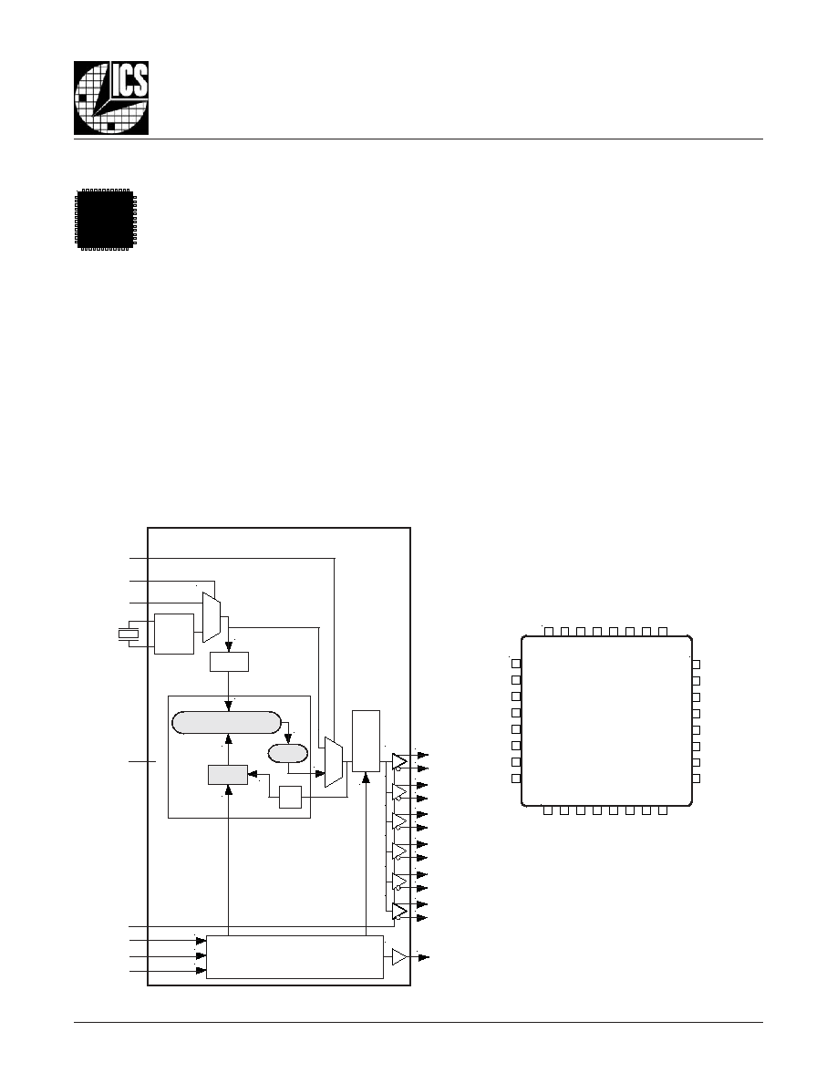
- Block Diagram
- Pin Assignment
- Functional Description
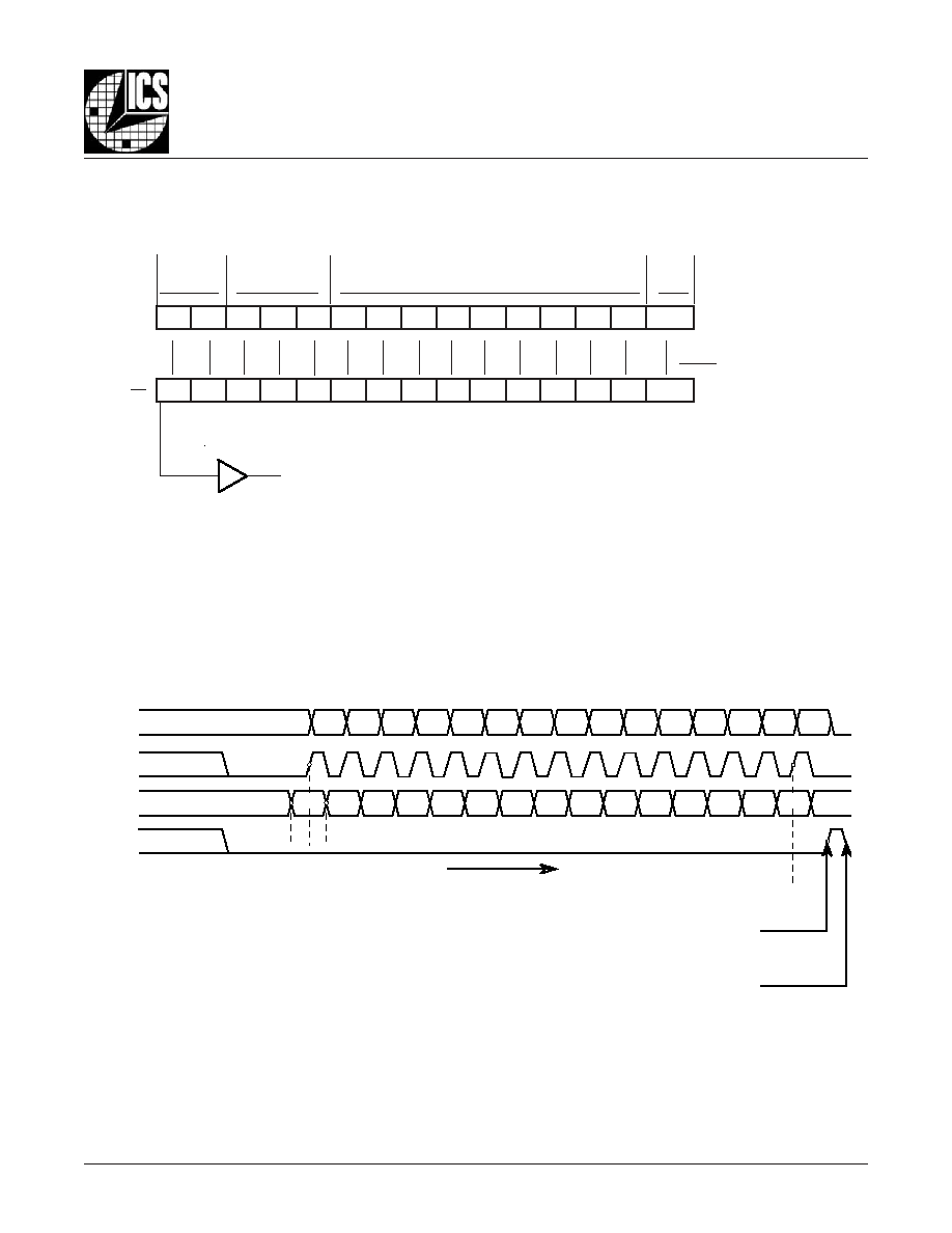
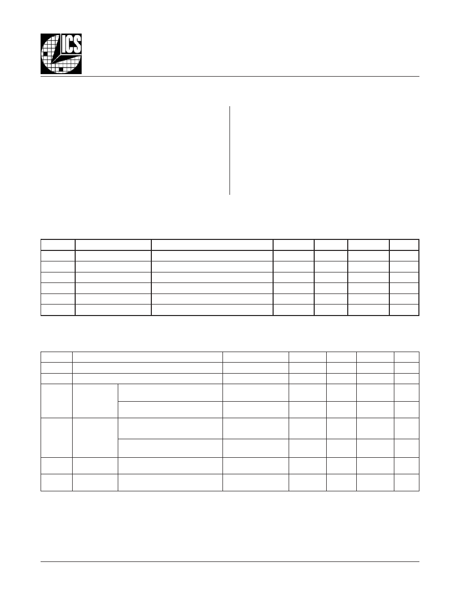
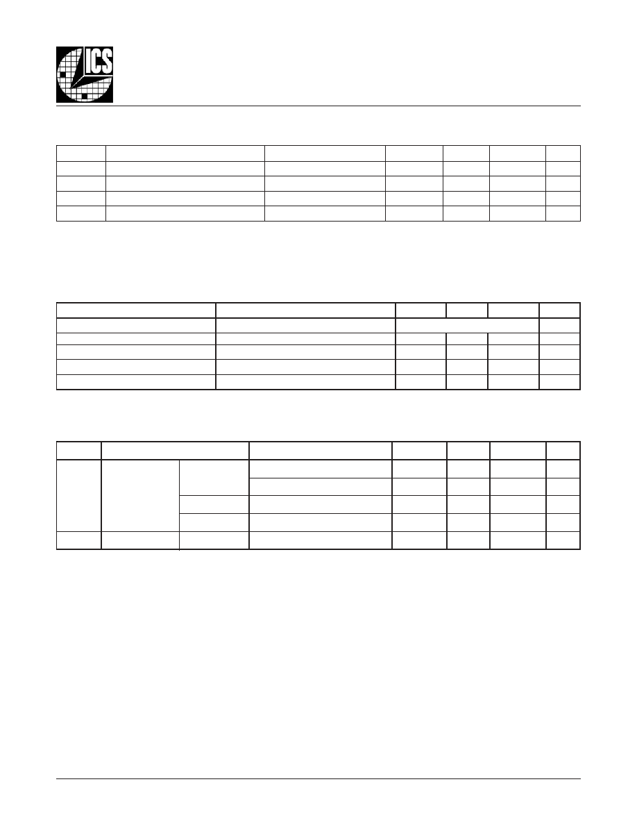
- Serial Load Operations Diagram
- M & N Dividers, SSC & Test Mode Control Bits Diagram
- Shift Register Operation Diagram
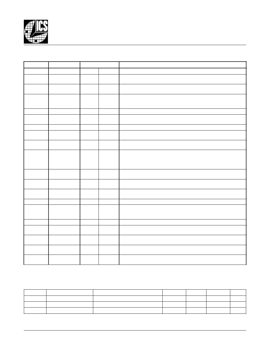
- Pin Descriptions
- Pin Characteristics
- Control Input Function Table
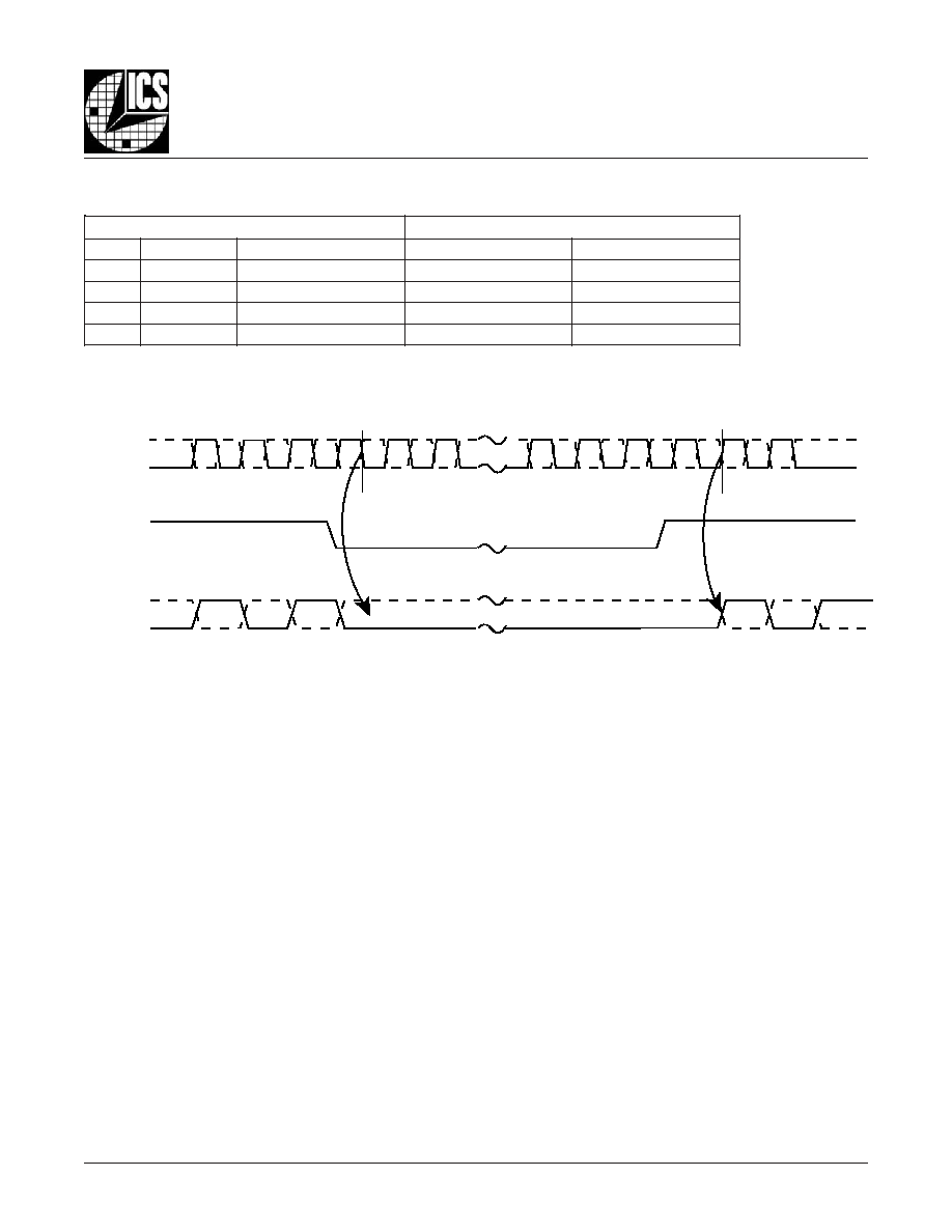
- OE Timing Diagram
- Programmable VCO Frequency Function Table
- Serial Mode Function Table
- Programmable Output Divider Function Table
- Absolute Maximum Ratings
- Power Supply DC Characteristics
- LVCMOS DC Characteristics
- LVHSTL DC Characteristics
- Crystal Characteristics
- Input Frequency Characteristics
- AC Characteristics
- Parameter Measurement Information
- Parameter Measurement Information, continued
- Application Information
- Recommendations for Unused Input and Output Pins
- Crystal Input Interface
- Power supply Filtering Techniques
- Spread Spectrum
- Layout Guideline
- Power Considerations
- Power Dissipation
- Junction Temperature
- Thermal Resistance for 32 Pin LQFP
- Thermal Resistance for 32 Pin VFQFN
- Calculations & Equations
- LVHSTL Driver Circuit & Termination Diagram
- Reliability Information
- Transistor Count
- Package Outline for 32 Lead LQFP
- Package Dimensions for 32 Lead LQFP
- Package Outline for 32 Lead VFQFN
- Package Dimensions for 32 Lead VFQFN
- Ordering Information
- Revision History Sheet
8427DY-02
www.icst.com/products/hiperclocks.html
REV. A FEBRUARY 17, 2006
1
Integrated
Circuit
Systems, Inc.
ICS8427-02
500MH
Z
, L
OW
J
ITTER
LVCMOS/C
RYSTAL
-
TO
-LVHSTL F
REQUENCY
S
YNTHESIZER
G
ENERAL
D
ESCRIPTION
The ICS8427-02 is a general purpose, six
LVHSTL output high frequency synthesizer
and a member of the HiPerClock STM family of
High Performance Clock Solutions from ICS.
The ICS8427-02 can suppor t a ver y wide
output frequency range of 15.625MHz to 500MHz. The
device powers up at a default output frequency of
200MHz with a 16.6667MHz crystal interface, and the
frequency can then be changed using the serial programm-
ing interface to change the M feedback divider and N
output divider. Frequency steps as small as 125kHz can
be achieved using a 16.6667MHz crystal and the output
divider set for
�16. The low jitter and frequency range of the
ICS8427-02 make it an ideal clock generator for most
clock tree applications.
F
EATURES
� Six differential LVHSTL outputs
� Selectable crystal input interface or TEST_CLK input
� TEST_CLK accepts the following input types:
LVCMOS, LVTTL
� Output frequency range: 15.625MHz to 500MHz
� VCO range: 250MHz to 500MHz
� Serial interface for programming feedback and output dividers
� Supports SSC, -0.5% downspread. Can be enabled through
use of the serial programming interface.
� Output skew: 100ps (maximum)
� Cycle-to-cycle jitter: 50ps (maximum)
� 2.5V core/1.8V output supply voltage
� 0�C to 70�C ambient operating temperature
� Industrial temperature information available upon request
� Available in both standard and lead-free RoHS-compliant
packages
HiPerClockSTM
ICS
B
LOCK
D
IAGRAM
32 31 30 29 28 27 26 25
9 10 11 12 13 14 15 16
1
2
3
4
5
6
7
8
24
23
22
21
20
19
18
17
XTAL_OUT
TEST_CLK
XTAL_SEL
V
DDA
S_LOAD
S_DATA
S_CLOCK
MR
V
DDO
FOUT2
nFOUT2
V
DDO
FOUT3
nFOUT3
OE
GND
GND
nFOUT5
FOUT5
V
DDO
nFOUT4
FOUT4
V
DD
TEST
XT
AL_IN
V
DD
VCO_SEL
FOUT0
nFOUT0
V
DDO
FOUT1
nFOUT1
32-Lead LQFP
7mm x 7mm x 1.4mm package body
Y Package
Top View
ICS8427-02
OSC
VCO_SEL
XTAL_SEL
TEST_CLK
XTAL_IN
XTAL_OUT
OE
S_LOAD
S_DATA
S_CLOCK
VCO
PLL
FOUT0
nFOUT0
FOUT1
nFOUT1
FOUT2
nFOUT2
FOUT3
nFOUT3
FOUT4
nFOUT4
FOUT5
nFOUT5
TEST
� 1,
� 2,
� 4,
� 8,
� 16
CONFIGURATION
INTERFACE
LOGIC
� M
0
1
0
1
� 16
PHASE DETECTOR
MR
� 2
32-Lead VFQFN
5mm x 5mm x 0.75mm package body
K Package
Top View
P
IN
A
SSIGNMENT

8427DY-02
www.icst.com/products/hiperclocks.html
REV. A FEBRUARY 17, 2006
2
Integrated
Circuit
Systems, Inc.
ICS8427-02
500MH
Z
, L
OW
J
ITTER
LVCMOS/C
RYSTAL
-
TO
-LVHSTL F
REQUENCY
S
YNTHESIZER
NOTE: The functional description that follows describes op-
eration using a 16.6667MHz crystal. Valid PLL loop divider
values for different crystal or input frequencies are defined in
the Input Frequency Characteristics, Table 6 NOTE 1.
The ICS8427-02 features a fully integrated PLL and therefore
requires no external components for setting the loop bandwidth.
A parallel-resonant, fundamental crystal is used as the input to
the on-chip oscillator. The output of the oscillator is divided by
16 prior to the phase detector. With a 16.6667MHz crystal, this
provides a 1.0417MHz reference frequency. The VCO of the
PLL operates over a range of 250MHz to 500MHz. The output of
the M divider is also applied to the phase detector.
The phase detector and the M divider force the VCO output fre-
quency to be 2M times the reference frequency by adjusting
the VCO control voltage. Note that for some values of M (either too
high or too low), the PLL will not achieve lock. The output of the
VCO is scaled by a divider prior to being sent to each of the LVPECL
output buffers. The divider provides a 50% output duty cycle.
The ICS8427-02 powers up by default to 200MHz output fre-
quency, using a 16.6667MHz crystal (M = 192, N = 2). The
output frequency can be changed after power-up by using the
serial interface to program the M feedback divider and the N
output divider.
The relationship between the VCO frequency, the crystal fre-
quency and the M divider is defined as follows:
The M value and the required values of M0 through M8 are shown
in Table 3B, Programmable VCO Frequency Function Table. Valid
M values for which the PLL will achieve lock for a 16.6667MHz
reference are defined as 120
M 240. The frequency out is
defined as follows:
Serial operation occurs when S_LOAD is LOW. The shift
register is loaded by sampling the S_DATA bits with the rising
edge of S_CLOCK. The contents of the shift register are
loaded into the M divider and N output divider when S_LOAD
transitions from LOW-to-HIGH. The M divide and N output
divide values are latched on the HIGH-to-LOW transition of
S_LOAD. If S_LOAD is held HIGH, data at the S_DATA input
is passed directly to the M divider and N outputdivider on each
rising edge of S_CLOCK. The serial mode can be used to
program the M and N bits and test bits T1 and T0. The internal
registers T0 and T1 determine the state of the TEST output
as follows:
F
UNCTIONAL
D
ESCRIPTION
N
fout = fVCO =
16
2M
fxtal x
N
16
fVCO =
fxtal x 2M
T1
T0
TEST Output
0
0
LOW
0
1
S_Data, Shift Register Input
1
0
Output of M divider
1
1
CMOS Fout
F
IGURE
1. S
ERIAL
L
OAD
O
PERATIONS
t
S
t
H
t
S
Time
S_CLOCK
S_DATA
S_LOAD
NOTE: Default Output Frequency, using a 16.6667MHz crystal
on power-up = 200MHz (M = 192, N = 2) SSC off
T1
T0
N2
N1
N0
M8
M7
M6
M5
M4
M3
M2
M1
M0
SSC
(Power-up
Default)
8427DY-02
www.icst.com/products/hiperclocks.html
REV. A FEBRUARY 17, 2006
3
Integrated
Circuit
Systems, Inc.
ICS8427-02
500MH
Z
, L
OW
J
ITTER
LVCMOS/C
RYSTAL
-
TO
-LVHSTL F
REQUENCY
S
YNTHESIZER
t
S
t
H
t
S
T1 T0 N2 N1 N0 M8 M7 M6 M5 M4 M3 M2 M1 M0 SSC
T1 T0 N2 N1 N0 M8 M7 M6 M5 M4 M3 M2 M1 M0 SSC
Time
M
AND
N D
IVIDERS
, SSC
AND
T
EST
M
ODE
C
ONTROL
B
ITS
1
T
0
T
2
N
1
N
0
N
8
M
7
M
6
M
5
M
4
M
3
M
2
M
1
M
0
M
C
S
S
Test Mode
Control Register
N Divider
M Divider
SSC Control
Register
S_DATA
TEST Output
T1:T0 = 01
Shift Register
Data transfer from shift register
to M and N dividers and SSC and
Test Control Bits on a low-to-high
transition of S_LOAD.
1
T
0
T
2
N
1
N
0
N
8
M
7
M
6
M
5
M
4
M
3
M
2
M
1
M
0
M
C
S
S
ICS8427-02 S
HIFT
R
EGISTER
O
PERATION
� R
EAD
B
ACK
C
APABILITY
1. Device powers up by default in Test Mode 01.
The Test Output in this case is wired to the shift register.
2. Shift in serial data stream and latch into M, N, T1, T0 and SSC Control Bits.
Shift in T1:T0=00, so that the TEST Output will be turned off after the bits are shifted in and latched.
Data transferred to M, N dividers, TEST and SSC Control Bits.
Changes to M, N, SSC and TEST mode bits take affect at this time.
Data latched into M, N Dividers, TEST and SSC control bits.
TEST Output
S_CLOCK
S_DATA
S_LOAD
8427DY-02
www.icst.com/products/hiperclocks.html
REV. A FEBRUARY 17, 2006
4
Integrated
Circuit
Systems, Inc.
ICS8427-02
500MH
Z
, L
OW
J
ITTER
LVCMOS/C
RYSTAL
-
TO
-LVHSTL F
REQUENCY
S
YNTHESIZER
T
ABLE
1. P
IN
D
ESCRIPTIONS
T
ABLE
2. P
IN
C
HARACTERISTICS
l
o
b
m
y
S
r
e
t
e
m
a
r
a
P
s
n
o
i
t
i
d
n
o
C
t
s
e
T
m
u
m
i
n
i
M
l
a
c
i
p
y
T
m
u
m
i
x
a
M
s
t
i
n
U
C
N
I
e
c
n
a
t
i
c
a
p
a
C
t
u
p
n
I
4
F
p
R
P
U
L
L
U
P
r
o
t
s
i
s
e
R
p
u
ll
u
P
t
u
p
n
I
1
5
k
R
N
W
O
D
L
L
U
P
r
o
t
s
i
s
e
R
n
w
o
d
ll
u
P
t
u
p
n
I
1
5
k
r
e
b
m
u
N
e
m
a
N
e
p
y
T
n
o
i
t
p
i
r
c
s
e
D
0
3
,
3
1
,
4
,
1
V
O
D
D
r
e
w
o
P
.
s
n
i
p
y
l
p
p
u
s
t
u
p
t
u
O
3
,
2
,
2
T
U
O
F
2
T
U
O
F
n
t
u
p
t
u
O
.
s
l
e
v
e
l
e
c
a
f
r
e
t
n
i
L
T
S
H
.
r
i
a
p
t
u
p
t
u
o
l
a
i
t
n
e
r
e
f
f
i
D
6
,
5
,
3
T
U
O
F
3
T
U
O
F
n
t
u
p
t
u
O
.
s
l
e
v
e
l
e
c
a
f
r
e
t
n
i
L
T
S
H
.
r
i
a
p
t
u
p
t
u
o
l
a
i
t
n
e
r
e
f
f
i
D
7
E
O
t
u
p
n
I
p
u
ll
u
P
.
d
e
l
b
a
n
e
e
r
a
s
t
u
p
t
u
o
e
h
t
,
H
G
I
H
n
e
h
W
.
e
l
b
a
n
e
t
u
p
t
u
o
h
g
i
H
e
v
i
t
c
A
.
h
g
i
H
=
x
T
U
O
F
n
,
w
o
L
=
x
T
U
O
F
,
W
O
L
n
e
h
W
.
s
l
e
v
e
l
e
c
a
f
r
e
t
n
i
L
T
T
V
L
/
S
O
M
C
V
L
6
1
,
8
D
N
G
r
e
w
o
P
.
d
n
u
o
r
g
y
l
p
p
u
s
r
e
w
o
P
9
T
S
E
T
t
u
p
t
u
O
.
n
o
i
t
a
r
e
p
o
f
o
e
d
o
m
l
a
i
r
e
s
e
h
t
n
i
E
V
I
T
C
A
s
i
h
c
i
h
w
t
u
p
t
u
o
t
s
e
T
.
s
l
e
v
e
l
e
c
a
f
r
e
t
n
i
L
T
T
V
L
/
S
O
M
C
V
L
6
2
,
0
1
V
D
D
r
e
w
o
P
.
s
n
i
p
y
l
p
p
u
s
e
r
o
C
2
1
,
1
1
,
4
T
U
O
F
4
T
U
O
F
n
t
u
p
t
u
O
.
s
l
e
v
e
l
e
c
a
f
r
e
t
n
i
L
T
S
H
.
r
i
a
p
t
u
p
t
u
o
l
a
i
t
n
e
r
e
f
f
i
D
5
1
,
4
1
,
5
T
U
O
F
5
T
U
O
F
n
t
u
p
t
u
O
.
s
l
e
v
e
l
e
c
a
f
r
e
t
n
i
L
T
S
H
.
r
i
a
p
t
u
p
t
u
o
l
a
i
t
n
e
r
e
f
f
i
D
7
1
R
M
t
u
p
n
I
n
w
o
d
ll
u
P
s
r
e
d
i
v
i
d
l
a
n
r
e
t
n
i
e
h
t
,
H
G
I
H
c
i
g
o
l
n
e
h
W
.
t
e
s
e
R
r
e
t
s
a
M
h
g
i
H
e
v
i
t
c
A
d
e
t
r
e
v
n
i
e
h
t
d
n
a
w
o
l
o
g
o
t
x
T
U
O
F
s
t
u
p
t
u
o
e
u
r
t
e
h
t
g
n
i
s
u
a
c
t
e
s
e
r
e
r
a
s
r
e
d
i
v
i
d
l
a
n
r
e
t
n
i
e
h
t
,
W
O
L
c
i
g
o
l
n
e
h
W
.
h
g
i
h
o
g
o
t
x
T
U
O
F
n
s
t
u
p
t
u
o
.
s
l
e
v
e
l
e
c
a
f
r
e
t
n
i
L
T
T
V
L
/
S
O
M
C
V
L
.
d
e
l
b
a
n
e
e
r
a
s
t
u
p
t
u
o
e
h
t
d
n
a
8
1
K
C
O
L
C
_
S
t
u
p
n
I
p
u
ll
u
P
.
r
e
t
s
i
g
e
r
t
f
i
h
s
e
h
t
o
t
n
i
A
T
A
D
_
S
l
a
i
r
e
s
d
a
o
l
o
t
k
c
o
l
c
t
u
p
n
I
.
s
l
e
v
e
l
e
c
a
f
r
e
t
n
i
L
T
T
V
L
/
S
O
M
C
V
L
9
1
A
T
A
D
_
S
t
u
p
n
I
p
u
ll
u
P
f
o
e
g
d
e
g
n
i
s
i
r
e
h
t
n
o
d
e
l
p
m
a
s
a
t
a
D
.
t
u
p
n
i
l
a
i
r
e
s
r
e
t
s
i
g
e
r
t
f
i
h
S
.
s
l
e
v
e
l
e
c
a
f
r
e
t
n
i
L
T
T
V
L
/
S
O
M
C
V
L
.
K
C
O
L
C
_
S
0
2
D
A
O
L
_
S
t
u
p
n
I
n
w
o
d
ll
u
P
.
s
r
e
d
i
v
i
d
e
h
t
o
t
n
i
r
e
t
s
i
g
e
r
t
f
i
h
s
m
o
r
f
a
t
a
d
f
o
n
o
i
t
i
s
n
a
r
t
s
l
o
r
t
n
o
C
.
s
l
e
v
e
l
e
c
a
f
r
e
t
n
i
L
T
T
V
L
/
S
O
M
C
V
L
1
2
V
A
D
D
r
e
w
o
P
.
n
i
p
y
l
p
p
u
s
g
o
l
a
n
A
2
2
L
E
S
_
L
A
T
X
t
u
p
n
I
p
u
ll
u
P
e
c
n
e
r
e
f
e
r
L
L
P
e
h
t
s
a
t
u
p
n
i
t
s
e
t
r
o
t
u
p
n
i
L
A
T
X
n
e
e
w
t
e
b
s
t
c
e
l
e
S
K
L
C
_
T
S
E
T
s
t
c
e
l
e
S
.
H
G
I
H
n
e
h
w
t
u
p
n
i
L
A
T
X
s
t
c
e
l
e
S
.
e
c
r
u
o
s
.
s
l
e
v
e
l
e
c
a
f
r
e
t
n
i
L
T
T
V
L
/
S
O
M
C
V
L
.
W
O
L
n
e
h
w
3
2
K
L
C
_
T
S
E
T
t
u
p
n
I
n
w
o
d
ll
u
P
.
s
l
e
v
e
l
e
c
a
f
r
e
t
n
i
L
T
T
V
L
/
S
O
M
C
V
L
.
t
u
p
n
i
k
c
o
l
c
t
s
e
T
5
2
,
4
2
,
T
U
O
_
L
A
T
X
N
I
_
L
A
T
X
t
u
p
n
I
.
t
u
p
n
i
e
h
t
s
i
N
I
_
L
A
T
X
.
e
c
a
f
r
e
t
n
i
r
o
t
a
ll
i
c
s
o
l
a
t
s
y
r
C
.
t
u
p
t
u
o
e
h
t
s
i
T
U
O
_
L
A
T
X
7
2
L
E
S
_
O
C
V
t
u
p
n
I
p
u
ll
u
P
.
e
d
o
m
s
s
a
p
y
b
r
o
L
L
P
n
i
s
i
r
e
z
i
s
e
h
t
n
y
s
r
e
h
t
e
h
w
s
e
n
i
m
r
e
t
e
D
.
s
l
e
v
e
l
e
c
a
f
r
e
t
n
i
L
T
T
V
L
/
S
O
M
C
V
L
9
2
,
8
2
,
0
T
U
O
F
0
T
U
O
F
n
t
u
p
t
u
O
.
s
l
e
v
e
l
e
c
a
f
r
e
t
n
i
L
T
S
H
.
r
i
a
p
t
u
p
t
u
o
l
a
i
t
n
e
r
e
f
f
i
D
2
3
,
1
3
,
1
T
U
O
F
1
T
U
O
F
n
t
u
p
t
u
O
.
s
l
e
v
e
l
e
c
a
f
r
e
t
n
i
L
T
S
H
.
r
i
a
p
t
u
p
t
u
o
l
a
i
t
n
e
r
e
f
f
i
D
:
E
T
O
N
p
u
ll
u
P
d
n
a
n
w
o
d
ll
u
P
.
s
e
u
l
a
v
l
a
c
i
p
y
t
r
o
f
,
s
c
i
t
s
i
r
e
t
c
a
r
a
h
C
n
i
P
,
2
e
l
b
a
T
e
e
S
.
s
r
o
t
s
i
s
e
r
t
u
p
n
i
l
a
n
r
e
t
n
i
o
t
r
e
f
e
r
8427DY-02
www.icst.com/products/hiperclocks.html
REV. A FEBRUARY 17, 2006
5
Integrated
Circuit
Systems, Inc.
ICS8427-02
500MH
Z
, L
OW
J
ITTER
LVCMOS/C
RYSTAL
-
TO
-LVHSTL F
REQUENCY
S
YNTHESIZER
Enabled
Disabled
nFOUT0:5
FOUT0:5
F
IGURE
2. OE T
IMING
D
IAGRAM
OE
nVCO
T
ABLE
3A. C
ONTROL
I
NPUT
F
UNCTION
T
ABLE
s
t
u
p
n
I
s
t
u
p
t
u
O
E
O
L
E
S
_
L
A
T
X
e
c
r
u
o
S
d
e
t
c
e
l
e
S
5
T
U
O
F
:
0
T
U
O
F
5
T
U
O
F
n
:
0
T
U
O
F
n
0
0
K
L
C
_
T
S
E
T
W
O
L
;
d
e
l
b
a
s
i
D
H
G
I
H
;
d
e
l
b
a
s
i
D
0
1
T
U
O
_
L
A
T
X
,
N
I
_
L
A
T
X
W
O
L
;
d
e
l
b
a
s
i
D
H
G
I
H
;
d
e
l
b
a
s
i
D
1
0
K
L
C
_
T
S
E
T
d
e
l
b
a
n
E
d
e
l
b
a
n
E
1
1
T
U
O
_
L
A
T
X
,
N
I
_
L
A
T
X
d
e
l
b
a
n
E
d
e
l
b
a
n
E
e
g
d
e
O
C
V
g
n
il
l
a
f
d
n
a
g
n
i
s
i
r
a
g
n
i
w
o
ll
o
f
d
e
l
b
a
n
e
r
o
d
e
l
b
a
s
i
d
e
r
a
s
t
u
p
t
u
o
k
c
o
l
c
e
h
t
,
s
e
h
c
t
i
w
s
E
O
r
e
t
f
A
n
i
n
w
o
h
s
s
a
.
2
e
r
u
g
i
F
VCO

8427DY-02
www.icst.com/products/hiperclocks.html
REV. A FEBRUARY 17, 2006
6
Integrated
Circuit
Systems, Inc.
ICS8427-02
500MH
Z
, L
OW
J
ITTER
LVCMOS/C
RYSTAL
-
TO
-LVHSTL F
REQUENCY
S
YNTHESIZER
T
ABLE
3B. P
ROGRAMMABLE
VCO F
REQUENCY
F
UNCTION
T
ABLE
NOTE 1
T
ABLE
3C. S
ERIAL
M
ODE
F
UNCTION
T
ABLE
T
ABLE
3D. P
ROGRAMMABLE
O
UTPUT
D
IVIDER
F
UNCTION
T
ABLE
t
u
p
n
I
e
u
l
a
V
r
e
d
i
v
i
D
N
)
z
H
M
(
y
c
n
e
u
q
e
r
F
t
u
p
t
u
O
2
N
1
N
0
N
m
u
m
i
n
i
M
m
u
m
i
x
a
M
0
0
0
2
5
2
1
0
5
2
0
0
1
4
5
.
2
6
5
2
1
0
1
0
8
5
2
.
1
3
5
.
2
6
0
1
1
6
1
5
2
6
.
5
1
5
2
.
1
3
1
0
0
1
0
5
2
0
0
5
1
0
1
2
5
2
1
0
5
2
1
1
0
4
5
.
2
6
5
2
1
1
1
1
8
5
2
.
1
3
5
.
2
6
y
c
n
e
u
q
e
r
F
O
C
V
)
z
H
M
(
e
d
i
v
i
D
M
6
5
2
8
2
1
4
6
2
3
6
1
8
4
2
1
8
M
7
M
6
M
5
M
4
M
3
M
2
M
1
M
0
M
0
5
2
0
2
1
0
0
1
1
1
1
0
0
0
8
0
.
2
5
2
1
2
1
0
0
1
1
1
1
0
0
1
7
1
.
4
5
2
2
2
1
0
0
1
1
1
1
0
1
0
�
�
�
�
�
�
�
�
�
�
�
0
0
4
2
9
1
0
1
1
0
0
0
0
0
0
�
�
�
�
�
�
�
�
�
�
�
2
9
.
7
9
4
9
3
2
0
1
1
1
0
1
1
1
1
0
0
5
0
4
2
0
1
1
1
1
0
0
0
0
.
z
H
M
7
6
6
6
.
6
1
f
o
y
c
n
e
u
q
e
r
f
t
u
p
n
i
n
a
o
t
d
n
o
p
s
e
r
r
o
c
s
e
i
c
n
e
u
q
e
r
f
g
n
i
t
l
u
s
e
r
e
h
t
d
n
a
s
e
u
l
a
v
e
d
i
v
i
d
M
e
s
e
h
T
:
1
E
T
O
N
s
t
u
p
n
I
s
n
o
i
t
i
d
n
o
C
R
M
D
A
O
L
_
S
K
C
O
L
C
_
S
A
T
A
D
_
S
H
X
X
X
.
h
g
i
H
=
x
T
U
O
F
n
,
w
o
L
=
x
T
U
O
F
.
W
O
L
l
a
i
t
n
e
r
e
f
f
i
d
s
t
u
p
t
u
o
s
e
c
r
o
F
.
t
e
s
e
R
L
L
X
X
n
o
i
t
i
s
n
a
r
t
W
O
L
t
x
e
n
li
t
n
u
d
e
d
a
o
l
s
n
i
a
m
e
r
d
n
a
s
r
e
t
s
i
g
e
r
t
u
p
n
i
o
t
n
i
d
e
h
c
t
a
l
s
i
a
t
a
D
.
s
r
u
c
c
o
t
n
e
v
e
l
a
i
r
e
s
a
li
t
n
u
r
o
L
L
a
t
a
D
g
n
i
s
i
r
h
c
a
e
n
o
A
T
A
D
_
S
n
o
a
t
a
d
h
t
i
w
d
e
d
a
o
l
s
i
r
e
t
s
i
g
e
r
t
f
i
h
S
.
e
d
o
m
t
u
p
n
i
l
a
i
r
e
S
.
K
C
O
L
C
_
S
f
o
e
g
d
e
L
L
a
t
a
D
.
r
e
d
i
v
i
d
t
u
p
t
u
o
N
d
n
a
r
e
d
i
v
i
d
M
e
h
t
o
t
d
e
s
s
a
p
e
r
a
r
e
t
s
i
g
e
r
t
f
i
h
s
e
h
t
f
o
s
t
n
e
t
n
o
C
L
L
a
t
a
D
.
d
e
h
c
t
a
l
e
r
a
s
e
u
l
a
v
r
e
d
i
v
i
d
t
u
p
t
u
o
N
d
n
a
r
e
d
i
v
i
d
M
L
L
X
X
.
s
r
e
t
s
i
g
e
r
t
f
i
h
s
t
c
e
f
f
a
t
o
n
o
d
t
u
p
n
i
l
a
i
r
e
S
L
H
a
t
a
D
.
d
e
k
c
o
l
c
s
i
t
i
s
a
r
e
d
i
v
i
d
M
o
t
y
l
t
c
e
r
i
d
d
e
s
s
a
p
A
T
A
D
_
S
W
O
L
=
L
:
E
T
O
N
H
G
I
H
=
H
e
r
a
c
t
'
n
o
D
=
X
n
o
i
t
i
s
n
a
r
t
e
g
d
e
g
n
i
s
i
R
=
n
o
i
t
i
s
n
a
r
t
e
g
d
e
g
n
il
l
a
F
=
8427DY-02
www.icst.com/products/hiperclocks.html
REV. A FEBRUARY 17, 2006
7
Integrated
Circuit
Systems, Inc.
ICS8427-02
500MH
Z
, L
OW
J
ITTER
LVCMOS/C
RYSTAL
-
TO
-LVHSTL F
REQUENCY
S
YNTHESIZER
T
ABLE
4A. P
OWER
S
UPPLY
DC C
HARACTERISTICS
,
V
DD
= V
DDA
= 2.5V�5%, V
DDO
= 1.8V�0.2V, T
A
= 0�C
TO
70�C
T
ABLE
4B. LVCMOS/LVTTL DC C
HARACTERISTICS
,
V
DD
= V
DDA
= 2.5V�5%, V
DDO
= 1.8V�0.2V, T
A
= 0�C
TO
70�C
l
o
b
m
y
S
r
e
t
e
m
a
r
a
P
s
n
o
i
t
i
d
n
o
C
t
s
e
T
m
u
m
i
n
i
M
l
a
c
i
p
y
T
m
u
m
i
x
a
M
s
t
i
n
U
V
H
I
e
g
a
t
l
o
V
h
g
i
H
t
u
p
n
I
7
.
1
V
D
D
3
.
0
+
V
V
L
I
e
g
a
t
l
o
V
w
o
L
t
u
p
n
I
3
.
0
-
7
.
0
V
I
H
I
t
u
p
n
I
t
n
e
r
r
u
C
h
g
i
H
K
L
C
_
T
S
E
T
,
D
A
O
L
_
S
,
R
M
V
D
D
V
=
N
I
V
5
2
6
.
2
=
0
5
1
A
�
,
L
E
S
_
O
C
V
,
L
E
S
_
L
A
T
X
E
O
,
A
T
A
D
_
S
,
K
C
O
L
C
_
S
V
D
D
V
=
N
I
V
5
2
6
.
2
=
5
A
�
I
L
I
t
u
p
n
I
t
n
e
r
r
u
C
w
o
L
K
L
C
_
T
S
E
T
,
D
A
O
L
_
S
,
R
M
V
D
D
=
V
5
2
6
.
2
,
V
N
I
V
0
=
5
-
A
�
,
L
E
S
_
O
C
V
,
L
E
S
_
L
A
T
X
E
O
,
A
T
A
D
_
S
,
K
C
O
L
C
_
S
V
D
D
=
,
V
5
2
6
.
2
V
N
I
V
0
=
0
5
1
-
A
�
V
H
O
t
u
p
t
u
O
e
g
a
t
l
o
V
h
g
i
H
1
E
T
O
N
;
T
S
E
T
5
.
1
V
V
L
O
t
u
p
t
u
O
e
g
a
t
l
o
V
w
o
L
1
E
T
O
N
;
T
S
E
T
4
.
0
V
0
5
h
t
i
w
d
e
t
a
n
i
m
r
e
t
s
t
u
p
t
u
O
:
1
E
T
O
N
V
o
t
O
D
D
.
2
/
NOTE: Stresses beyond those listed under Absolute
Maximum Ratings may cause permanent damage to the
device. These ratings are stress specifications only. Functional
operation of product at these conditions or any conditions be-
yond those listed in the
DC Characteristics
or
AC Character-
istics
is not implied. Exposure to absolute maximum rating
conditions for extended periods may affect product reliability.
A
BSOLUTE
M
AXIMUM
R
ATINGS
Supply Voltage, V
DD
4.6V
Inputs, V
I
-0.5V to V
DD
+ 0.5V
Outputs, I
O
Continuous Current
50mA
Surge Current
100mA
Package Thermal Impedance,
JA
for 32 Lead LQFP
47.9�C/W (0 lfpm)
for 32 Lead VFQFN
34.8�C/W (0 lfpm)
Storage Temperature, T
STG
-65�C to 150�C
l
o
b
m
y
S
r
e
t
e
m
a
r
a
P
s
n
o
i
t
i
d
n
o
C
t
s
e
T
m
u
m
i
n
i
M
l
a
c
i
p
y
T
m
u
m
i
x
a
M
s
t
i
n
U
V
D
D
y
l
p
p
u
S
e
r
o
C
5
7
3
.
2
5
.
2
5
2
6
.
2
V
V
A
D
D
e
g
a
t
l
o
V
g
o
l
a
n
A
5
7
3
.
2
5
.
2
5
2
6
.
2
V
V
O
D
D
e
g
a
t
l
o
V
t
u
p
t
u
O
6
.
1
8
.
1
0
.
2
V
I
D
D
t
n
e
r
r
u
C
y
l
p
p
u
S
r
e
w
o
P
5
7
1
A
m
I
A
D
D
t
n
e
r
r
u
C
y
l
p
p
u
S
g
o
l
a
n
A
5
1
A
m
I
0
D
D
t
n
e
r
r
u
C
y
l
p
p
u
S
t
u
p
t
u
O
d
a
o
L
o
N
0
A
m
8427DY-02
www.icst.com/products/hiperclocks.html
REV. A FEBRUARY 17, 2006
8
Integrated
Circuit
Systems, Inc.
ICS8427-02
500MH
Z
, L
OW
J
ITTER
LVCMOS/C
RYSTAL
-
TO
-LVHSTL F
REQUENCY
S
YNTHESIZER
T
ABLE
6. I
NPUT
C
HARACTERISTICS
,
V
DD
= V
DDA
= 2.5V�5%, V
DDO
= 1.8V�0.2V, T
A
= 0�C
TO
70�C
T
ABLE
5. C
RYSTAL
C
HARACTERISTICS
r
e
t
e
m
a
r
a
P
s
n
o
i
t
i
d
n
o
C
t
s
e
T
m
u
m
i
n
i
M
l
a
c
i
p
y
T
m
u
m
i
x
a
M
s
t
i
n
U
n
o
i
t
a
ll
i
c
s
O
f
o
e
d
o
M
l
a
t
n
e
m
a
d
n
u
F
y
c
n
e
u
q
e
r
F
2
1
0
4
z
H
M
)
R
S
E
(
e
c
n
a
t
s
i
s
e
R
s
e
i
r
e
S
t
n
e
l
a
v
i
u
q
E
0
5
e
c
n
a
t
i
c
a
p
a
C
t
n
u
h
S
7
F
p
l
e
v
e
L
e
v
i
r
D
1
W
m
T
ABLE
4C. LVHSTL DC C
HARACTERISTICS
,
V
DD
= V
DDA
= 2.5V�5%, V
DDO
= 1.8V�0.2V, T
A
= 0�C
TO
70�C
l
o
b
m
y
S
r
e
t
e
m
a
r
a
P
s
n
o
i
t
i
d
n
o
C
t
s
e
T
m
u
m
i
n
i
M
l
a
c
i
p
y
T
m
u
m
i
x
a
M
s
t
i
n
U
V
H
O
1
E
T
O
N
;
e
g
a
t
l
o
V
h
g
i
H
t
u
p
t
u
O
9
.
0
3
.
1
V
V
L
O
1
E
T
O
N
;
e
g
a
t
l
o
V
w
o
L
t
u
p
t
u
O
0
4
.
0
V
V
X
O
2
E
T
O
N
;
e
g
a
t
l
o
V
r
e
v
o
s
s
o
r
C
t
u
p
t
u
O
0
4
0
6
%
V
G
N
I
W
S
g
n
i
w
S
e
g
a
t
l
o
V
t
u
p
t
u
O
k
a
e
P
-
o
t
-
k
a
e
P
6
.
0
1
.
1
V
0
5
h
t
i
w
d
e
t
a
n
i
m
r
e
t
s
t
u
p
t
u
O
:
1
E
T
O
N
V
5
.
2
e
e
S
.
D
N
G
o
t
e
r
u
g
i
f
t
i
u
c
r
i
C
t
s
e
T
d
a
o
L
t
u
p
t
u
O
e
h
t
n
i
.
n
o
i
t
c
e
s
n
o
i
t
a
m
r
o
f
n
I
t
n
e
m
e
r
u
s
a
e
M
r
e
t
e
m
a
r
a
P
.
n
o
i
t
i
d
n
o
c
n
e
v
i
g
a
t
a
g
n
i
w
s
e
g
a
t
l
o
v
t
u
p
t
u
o
o
t
t
c
e
p
s
e
r
h
t
i
w
d
e
n
i
f
e
D
:
2
E
T
O
N
l
o
b
m
y
S
r
e
t
e
m
a
r
a
P
s
n
o
i
t
i
d
n
o
C
t
s
e
T
m
u
m
i
n
i
M
l
a
c
i
p
y
T
m
u
m
i
x
a
M
s
t
i
n
U
f
N
I
y
c
n
e
u
q
e
r
F
t
u
p
n
I
K
L
C
_
T
S
E
T
1
=
t
c
e
l
e
s
O
C
V
2
1
0
4
z
H
M
)
e
d
o
m
s
s
a
p
y
b
(
0
=
t
c
e
l
e
s
O
C
V
0
0
4
z
H
M
1
E
T
O
N
;
L
A
T
X
2
1
0
4
z
H
M
K
C
O
L
C
_
S
0
5
z
H
M
t
T
U
P
N
I
_
r
e
m
i
T
e
s
i
R
t
u
p
n
I
K
L
C
_
T
S
E
T
5
s
n
y
c
n
e
u
q
e
r
f
O
C
V
m
u
m
i
x
a
m
r
o
m
u
m
i
n
i
m
e
h
t
e
v
e
i
h
c
a
o
t
t
e
s
e
b
t
s
u
m
e
u
l
a
v
M
e
h
t
e
g
n
a
r
y
c
n
e
u
q
e
r
f
l
a
t
s
y
r
c
e
h
t
r
o
F
:
1
E
T
O
N
7
6
1
e
r
a
M
f
o
s
e
u
l
a
v
d
il
a
v
z
H
M
2
1
f
o
y
c
n
e
u
q
e
r
f
m
u
m
i
n
i
m
e
h
t
g
n
i
s
U
.
z
H
M
0
0
5
r
o
z
H
M
0
5
2
f
o
e
g
n
a
r
M
6
5
2
.
e
h
t
g
n
i
s
U
0
5
e
r
a
M
f
o
s
e
u
l
a
v
d
il
a
v
z
H
M
0
4
f
o
y
c
n
e
u
q
e
r
f
m
u
m
i
x
a
m
M
.
0
0
1
8427DY-02
www.icst.com/products/hiperclocks.html
REV. A FEBRUARY 17, 2006
9
Integrated
Circuit
Systems, Inc.
ICS8427-02
500MH
Z
, L
OW
J
ITTER
LVCMOS/C
RYSTAL
-
TO
-LVHSTL F
REQUENCY
S
YNTHESIZER
T
ABLE
7. AC C
HARACTERISTICS
,
V
DD
= V
DDA
= 2.5V�5%, V
DDO
= 1.8V�0.2V, T
A
= 0�C
TO
70�C
l
o
b
m
y
S
r
e
t
e
m
a
r
a
P
s
n
o
i
t
i
d
n
o
C
t
s
e
T
m
u
m
i
n
i
M
l
a
c
i
p
y
T
m
u
m
i
x
a
M
s
t
i
n
U
F
X
A
M
y
c
n
e
u
q
e
r
F
t
u
p
t
u
O
0
0
5
z
H
M
t
)
c
c
(
t
ij
3
,
1
E
T
O
N
;
r
e
t
t
i
J
e
l
c
y
C
-
o
t
-
e
l
c
y
C
F
T
U
O
z
H
M
0
0
2
=
0
3
0
5
s
p
F
T
U
O
z
H
M
7
6
2
=
0
3
0
5
s
p
F
T
U
O
z
H
M
3
3
3
=
0
3
0
5
s
p
F
T
U
O
z
H
M
0
0
4
=
0
3
0
5
s
p
t
)
0
5
T
(
t
t
ij
r
e
t
t
i
J
e
l
c
y
C
0
5
T
F
T
U
O
z
H
M
0
0
2
=
0
0
2
s
p
F
T
U
O
z
H
M
7
6
2
=
0
0
2
s
p
F
T
U
O
z
H
M
3
3
3
=
0
0
2
s
p
F
T
U
O
z
H
M
0
0
4
=
0
0
2
s
p
t
)
r
e
p
(
t
ij
1
E
T
O
N
;
S
M
R
,
r
e
t
t
i
J
d
o
i
r
e
P
5
.
2
5
s
p
t
)
o
(
k
s
3
,
2
E
T
O
N
;
w
e
k
S
t
u
p
t
u
O
5
6
0
0
1
s
p
F
M
5
,
4
E
T
O
N
;
y
c
n
e
u
q
e
r
F
n
o
i
t
a
l
u
d
o
M
C
S
S
F
T
U
O
z
H
M
0
0
2
=
0
3
3
3
.
3
3
z
H
k
F
T
U
O
z
H
M
7
6
2
=
0
3
3
3
.
3
3
z
H
k
F
T
U
O
z
H
M
3
3
3
=
0
3
3
3
.
3
3
z
H
k
F
T
U
O
z
H
M
0
0
4
=
0
3
3
3
.
3
3
z
H
k
F
F
M
5
,
4
E
T
O
N
;
r
o
t
c
a
F
n
o
i
t
a
l
u
d
o
M
C
S
S
F
T
U
O
z
H
M
0
0
2
=
3
.
0
6
.
0
%
F
T
U
O
z
H
M
7
6
2
=
4
.
0
6
.
0
%
F
T
U
O
z
H
M
3
3
3
=
3
.
0
6
.
0
%
F
T
U
O
z
H
M
0
0
4
=
3
.
0
6
.
0
%
C
S
S
d
e
r
5
,
4
E
T
O
N
;
n
o
i
t
c
u
d
e
R
l
a
r
t
c
e
p
S
F
T
U
O
z
H
M
0
0
2
=
7
-
0
1
-
B
d
F
T
U
O
z
H
M
7
6
2
=
7
-
2
1
-
B
d
F
T
U
O
z
H
M
3
3
3
=
7
-
1
1
-
B
d
F
T
U
O
z
H
M
0
0
4
=
7
-
2
1
-
B
d
f
e
R
r
u
p
s
r
u
p
S
e
c
n
e
r
e
f
e
R
F
T
U
O
z
H
M
0
0
2
=
0
4
-
B
d
F
T
U
O
z
H
M
7
6
2
=
0
4
-
B
d
F
T
U
O
z
H
M
3
3
3
=
5
4
-
B
d
F
T
U
O
z
H
M
0
0
4
=
0
5
-
B
d
t
R
t
/
F
e
m
i
T
ll
a
F
/
e
s
i
R
t
u
p
t
u
O
%
0
8
o
t
%
0
2
3
3
3
7
6
6
s
p
t
S
e
m
i
T
p
u
t
e
S
K
C
O
L
C
_
S
o
t
A
T
A
D
_
S
5
s
n
D
A
O
L
_
S
o
t
K
C
O
L
C
_
S
5
s
n
t
H
e
m
i
T
d
l
o
H
K
C
O
L
C
_
S
o
t
A
T
A
D
_
S
5
s
n
D
A
O
L
_
S
o
t
K
C
O
L
C
_
S
5
s
n
c
d
o
e
l
c
y
C
y
t
u
D
t
u
p
t
u
O
1
=
N
0
4
0
6
%
2
=
N
5
4
5
5
%
t
K
C
O
L
e
m
i
T
k
c
o
L
L
L
P
1
s
m
.
n
o
i
t
c
e
s
n
o
i
t
a
m
r
o
f
n
I
t
n
e
m
e
r
u
s
a
e
M
r
e
t
e
m
a
r
a
P
e
e
S
.
s
t
u
p
n
i
L
A
T
X
g
n
i
s
u
e
c
n
a
m
r
o
f
r
e
p
r
e
t
t
i
J
:
1
E
T
O
N
.
s
n
o
i
t
i
d
n
o
c
d
a
o
l
l
a
u
q
e
h
t
i
w
d
n
a
e
g
a
t
l
o
v
y
l
p
p
u
s
e
m
a
s
e
h
t
t
a
s
t
u
p
t
u
o
n
e
e
w
t
e
b
w
e
k
s
s
a
d
e
n
i
f
e
D
:
2
E
T
O
N
.
s
t
n
i
o
p
s
s
o
r
c
l
a
i
t
n
e
r
e
f
f
i
d
t
u
p
t
u
o
e
h
t
t
a
d
e
r
u
s
a
e
M
.
5
6
d
r
a
d
n
a
t
S
C
E
D
E
J
h
t
i
w
e
c
n
a
d
r
o
c
c
a
n
i
d
e
n
i
f
e
d
s
i
r
e
t
e
m
a
r
a
p
s
i
h
T
:
3
E
T
O
N
.
d
e
l
b
a
n
e
g
n
i
k
c
o
l
c
m
u
r
t
c
e
p
S
d
a
e
r
p
S
:
4
E
T
O
N
.
l
a
t
s
y
r
c
z
t
r
a
u
q
z
H
M
7
6
6
6
.
6
1
a
g
n
i
s
U
:
5
E
T
O
N
8427DY-02
www.icst.com/products/hiperclocks.html
REV. A FEBRUARY 17, 2006
10
Integrated
Circuit
Systems, Inc.
ICS8427-02
500MH
Z
, L
OW
J
ITTER
LVCMOS/C
RYSTAL
-
TO
-LVHSTL F
REQUENCY
S
YNTHESIZER
P
ARAMETER
M
EASUREMENT
I
NFORMATION
T50 C
YCLE
-
TO
-C
YCLE
J
ITTER
S
PUR
R
EDUCTION
P
ERIOD
J
ITTER
O
UTPUT
S
KEW
C
YCLE
-
TO
-C
YCLE
J
ITTER
2.5V C
ORE
/1.8V O
UTPUT
L
OAD
AC T
EST
C
IRCUIT
SCOPE
LVHSTL
Qx
nQx
2.5V�5%
0V
t
sk(o)
nFOUTx
FOUTx
nFOUTy
FOUTy
t
jit(cc) =
t
cycle n �
t
cycle n+1
1000 Cycles
t
cycle n
t
cycle n+1
FOUT0:5
nFOUT0:5
V
OH
V
REF
V
OL
Mean Period
(First edge after trigger)
Reference Point
(Trigger Edge)
1
contains 68.26% of all measurements
2
contains 95.4% of all measurements
3
contains 99.73% of all measurements
4
contains 99.99366% of all measurements
6
contains (100-1.973x10
-7
)% of all measurements
Histogram
V
DD
GND
V
DDO
1.8V�0.2V
t
jit (50) = Period n � Period n +50
Minimum 16,667 consective cycles
334 measurements
Period n
Period n + 50
Period n
+ 50 + 50
Frequency
dBm
Reference Spur
FOUT0:5
nFOUT0:5
V
DDA
= 2.5V�5%

8427DY-02
www.icst.com/products/hiperclocks.html
REV. A FEBRUARY 17, 2006
11
Integrated
Circuit
Systems, Inc.
ICS8427-02
500MH
Z
, L
OW
J
ITTER
LVCMOS/C
RYSTAL
-
TO
-LVHSTL F
REQUENCY
S
YNTHESIZER
Clock
Outputs
20%
80%
80%
20%
t
R
t
F
V
SW I N G
t
PW
t
PERIOD
t
PW
t
PERIOD
odc =
x 100%
FOUT0:5
nFOUT0:5
60%
50%
V
O H
V
O L
40%
V
OX
O
UTPUT
C
ROSSOVER
V
OLTAGE
O
UTPUT
R
ISE
/F
ALL
T
IME
O
UTPUT
D
UTY
C
YCLE
/P
ULSE
W
IDTH
/P
ERIOD
FOUT0:5
nFOUT0:5
8427DY-02
www.icst.com/products/hiperclocks.html
REV. A FEBRUARY 17, 2006
12
Integrated
Circuit
Systems, Inc.
ICS8427-02
500MH
Z
, L
OW
J
ITTER
LVCMOS/C
RYSTAL
-
TO
-LVHSTL F
REQUENCY
S
YNTHESIZER
A
PPLICATION
I
NFORMATION
C
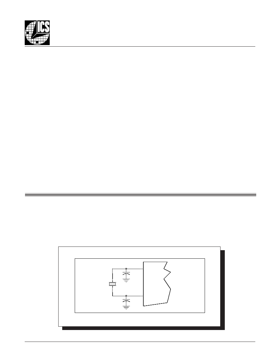
RYSTAL
I
NPUT
I
NTERFACE
The ICS8427-02 has been characterized with 18pF parallel
resonant crystals. The capacitor values, C1 and C2, shown in
Figure 3
below were determined using a 16.66MHz, 18pF
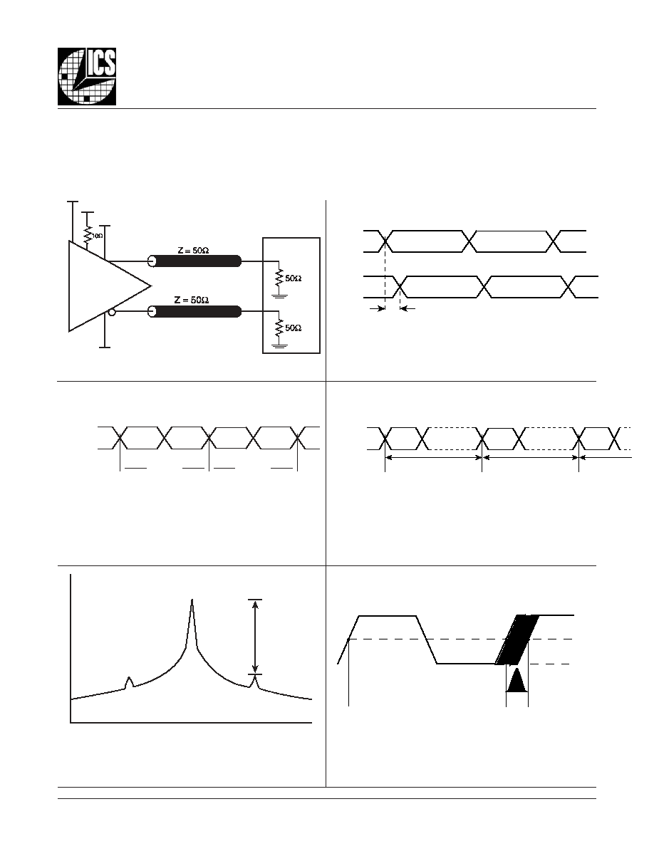
Figure 3. C
RYSTAL
I
NPU
t I
NTERFACE
parallel resonant crystal and were chosen to minimize the
ppm error. The optimum C1 and C2 values can be slightly
adjusted for different board layouts.
C1
22p
X1
18pF Parallel Crystal
C2
22p
XTAL_OUT
XTAL_IN
I
NPUTS
:
C
RYSTAL
I
NPUT
:
For applications not requiring the use of the crystal oscillator
input, both XTAL_IN and XTAL_OUT can be left floating.
Though not required, but for additional protection, a 1k
resistor can be tied from XTAL_IN to ground.
TEST_CLK I
NPUT
:
For applications not requiring the use of the test clock, it can
be left floating. Though not required, but for additional
protection, a 1k
resistor can be tied from the TEST_CLK to
ground.
LVCMOS C
ONTROL
P
INS
:
All control pins have internal pull-ups or pull-downs; additional
resistance is not required but can be added for additional
protection. A 1k
resistor can be used.
R
ECOMMENDATIONS
FOR
U
NUSED
I
NPUT
AND
O
UTPUT
P
INS
O
UTPUTS
:
LVHSTL O
UTPUT
All unused LVHSTL outputs can be left floating. We recommend
that there is no trace attached. Both sides of the differential
output pair should either be left floating or terminated.
8427DY-02
www.icst.com/products/hiperclocks.html
REV. A FEBRUARY 17, 2006
13
Integrated
Circuit
Systems, Inc.
ICS8427-02
500MH
Z
, L
OW
J
ITTER
LVCMOS/C
RYSTAL
-
TO
-LVHSTL F
REQUENCY
S
YNTHESIZER
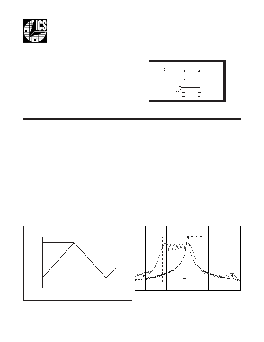
Spread-spectrum clocking is a frequency modulation tech-
nique for EMI reduction. When spread-spectrum is enabled, a
32.55kHz triangle waveform is used with 0.5% down-spread
(+0.0% / -0.5%) from the nominal 200MHz clock frequency.
An example of a triangle frequency modulation profile is shown
in
Figure 5A
below. The ramp profile can be expressed as:
� Fnom = Nominal Clock Frequency in Spread OFF mode
(200MHz with 16.6667MHz IN)
� Fm = Nominal Modulation Frequency
= Reference Frequency
16 x 32
�
= Modulation Factor (0.5% down spread)
(1 -
) fnom + 2 fm x x fnom x t when 0 < t <
,
(1 -
) fnom - 2 fm x x fnom x t when
< t <
1
2 fm
1
2 fm
1
fm
The ICS8427-02 triangle modulation frequency deviation will
not exceed 0.6% down-spread from the nominal clock fre-
quency (+0.0% / -0.5%). An example of the amount of down
spread relative to the nominal clock frequency can be seen in
the frequency domain, as shown in
Figure 5B.
The ratio of this
width to the fundamental frequency is typically 0.4%, and will
not exceed 0.6%. The resulting spectral reduction will be
greater than 7dB, as shown in Figure 5B. It is important to
note the ICS8427-02 7dB minimum spectral reduction is the
component-specific EMI reduction, and will not necessarily
be the same as the system EMI reduction.
F
IGURE
5B. 200MH
Z
C
LOCK
O
UTPUT
IN
F
REQUENCY
D
OMAIN
(A) S
PREAD
-S
PECTRUM
OFF
(B) S
PREAD
-S
PECTRUM
ON
F
IGURE
5A. T
RIANGLE
F
REQUENCY
M
ODULATION
S
PREAD
S
PECTRUM
Fnom
(1 -
) Fnom
0.5/fm
1/fm
As in any high speed analog circuitry, the power supply pins
are vulnerable to random noise. The ICS8427-02 provides
separate power supplies to isolate any high switching
noise from the outputs to the internal PLL. V
DD
, V
DDA
, and V
DDO
should be individually connected to the power supply
plane through vias, and bypass capacitors should be
used for each pin. To achieve optimum jitter performance,
power supply isolation is required.
Figure 4
illustrates how
a 10
resistor along with a 10F and a .01F bypass
capacitor should be connected to each V
DDA
pin.
P
OWER
S
UPPLY
F
ILTERING
T
ECHNIQUES
F
IGURE
4. P
OWER
S
UPPLY
F
ILTERING
10
V
DDA
10
F
.01
F
2.5V
.01
F
V
DD
B
A
- 10 dBm
= 0.3%
8427DY-02
www.icst.com/products/hiperclocks.html
REV. A FEBRUARY 17, 2006
14
Integrated
Circuit
Systems, Inc.
ICS8427-02
500MH
Z
, L
OW
J
ITTER
LVCMOS/C
RYSTAL
-
TO
-LVHSTL F
REQUENCY
S
YNTHESIZER
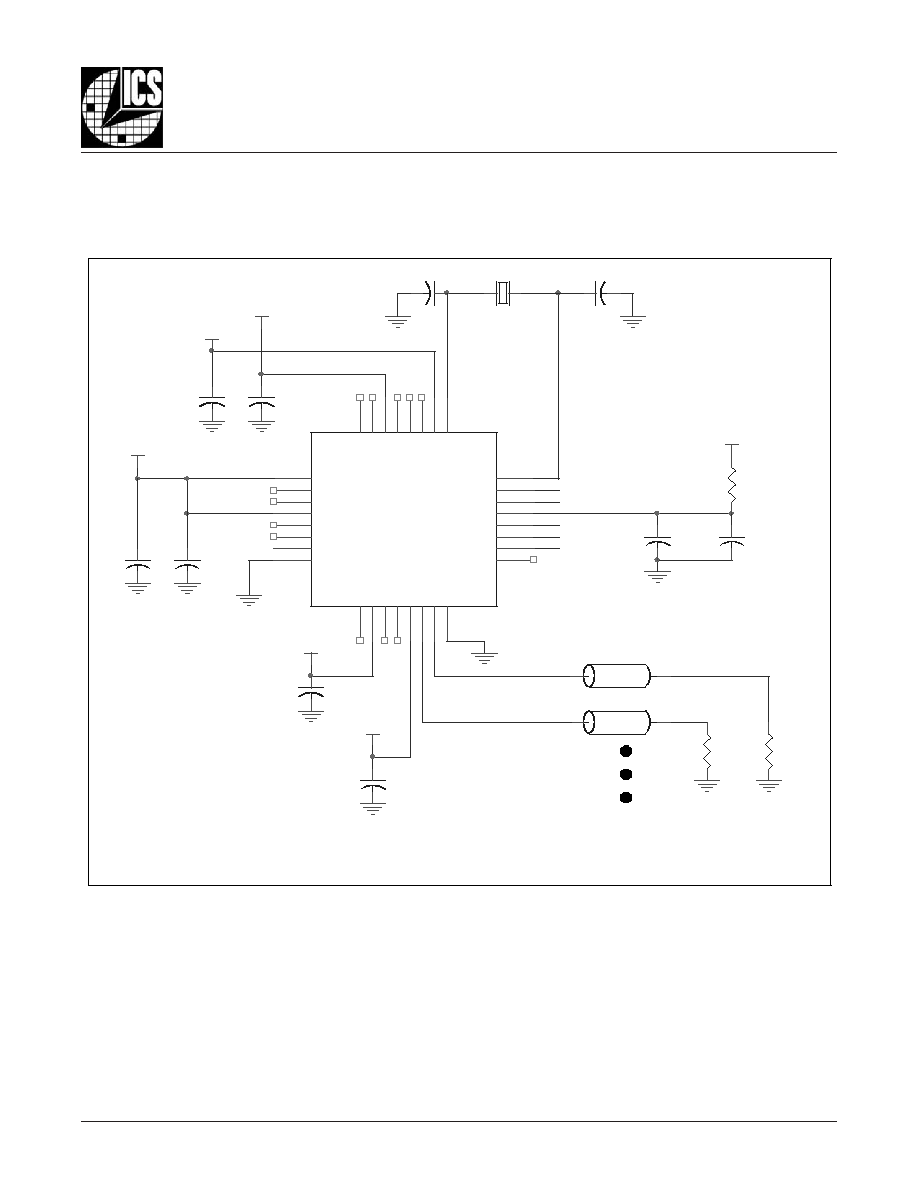
Figure 6 shows an application schematic example of the
ICS8427-02. In this example, a 16.6667MHz, 18 pF parallel
resonant crystal is used. The C1=22pF and C2=22pF are
L
AYOUT
G
UIDELINE
F
IGURE
6. S
CHEMATIC
OF
R
ECOMMENDED
L
AYOUT
approximate values for frequency accuracy. The C1 and C2
may be slightly adjusted for optimizing frequency accuracy.
C1
22p
C2
22p
VDD = 2.5V
VDDO = 1.8V
C7
0.1u
C6
0.1u
VDDO = 1.8V
VDDO = 1.8V
Zo = 50
Zo = 50
XTAL_SEL
TEST CLK
R2
50
R3
50
C9
0.1uF
U1
ICS8427-02
1
2
3
4
5
6
7
8
9
10
11
12
13
14
15
16
17
18
19
20
21
22
23
24
32
31
30
29
28
27
26
25
VDDO
FOUT2
nFOUT2
VDDO
FOUT3
nFOUT3
OE
GND
TE
S
T
VD
D
FO
U
T4
nF
O
U
T
4
V
DDO
FO
U
T5
nF
O
U
T
5
GN
D
MR
S_CLOCK
S_DATA
S_LOAD
VDDA
XTAL_SEL
TEST CLK
XTAL2
nF
O
U
T
1
FO
U
T
1
VD
D
O
nF
O
U
T
0
FO
U
T
0
VC
O
_
SEL
VD
D
XT
A
L
1
VDD = 2.5V
S_CLOCK
C10
0.1u
C5
0.1u
X1
16.6667MHz, 18pF
C8
0.1u
C4
10u
VDD = 2.5V
S_LOAD
R1
10
C3
0.01u
S_DATA

8427DY-02
www.icst.com/products/hiperclocks.html
REV. A FEBRUARY 17, 2006
15
Integrated
Circuit
Systems, Inc.
ICS8427-02
500MH
Z
, L
OW
J
ITTER
LVCMOS/C
RYSTAL
-
TO
-LVHSTL F
REQUENCY
S
YNTHESIZER
P
OWER
C
ONSIDERATIONS
This section provides information on power dissipation and junction temperature for the ICS8427-02.
Equations and example calculations are also provided.
1. Power Dissipation.
The total power dissipation for the ICS8427-02 is the sum of the core power plus the power dissipated in the load(s).
The following is the power dissipation for V
DD
= 2.5V + 5% = 2.625V, which gives worst case results.
NOTE: Please refer to Section 3 for details on calculating power dissipated in the load.
�
Power (core)
MAX
= V
DD_MAX
* I
DD_MAX
= 2.625V * 175mA = 459.4mW
�
Power (outputs)
MAX
= 32.6mW/Loaded Output pair
If all outputs are loaded, the total power is 6 * 32.6mW = 195.6mW
Total Power
_MAX
(3.465V, with all outputs switching) = 459.37mW + 195.6mW = 655mW
2. Junction Temperature.
Junction temperature, Tj, is the temperature at the junction of the bond wire and bond pad and directly affects the reliability of the
device. The maximum recommended junction temperature for HiPerClockS
TM
devices is 125�C.
The equation for Tj is as follows: Tj =
JA
* Pd_total + T
A
Tj = Junction Temperature
JA
= Junction-to-Ambient Thermal Resistance
Pd_total = Total Device Power Dissipation (example calculation is in section 1 above)
T
A
= Ambient Temperature
In order to calculate junction temperature, the appropriate junction-to-ambient thermal resistance
JA
must be used. Assuming a
moderate air flow of 200 linear feet per minute and a multi-layer board, the appropriate value is 42.1�C/W per Table 8A below.
Therefore, Tj for an ambient temperature of 70�C with all outputs switching is:
70�C + 0.655W * 42.1�C/W = 97.6�C. This is well below the limit of 125�C.
This calculation is only an example. Tj will obviously vary depending on the number of loaded outputs, supply voltage, air flow,
and the type of board (single layer or multi-layer).
JA
by Velocity (Linear Feet per Minute)
0
200
500
Single-Layer PCB, JEDEC Standard Test Boards
67.8�C/W
55.9�C/W
50.1�C/W
Multi-Layer PCB, JEDEC Standard Test Boards
47.9�C/W
42.1�C/W
39.4�C/W
NOTE: Most modern PCB designs use multi-layered boards. The data in the second row pertains to most designs.
T
ABLE
8A. T
HERMAL
R
ESISTANCE
JA
FOR
32-P
IN
LQFP, F
ORCED
C
ONVECTION
T
ABLE
8B.
JA
VS
. A
IR
F
LOW
T
ABLE
FOR
A
32 L
EAD
VFQFN
JA
by Velocity (Linear Feet per Minute)
0
Multi-Layer PCB, JEDEC Standard Test Boards
34.8�C/W
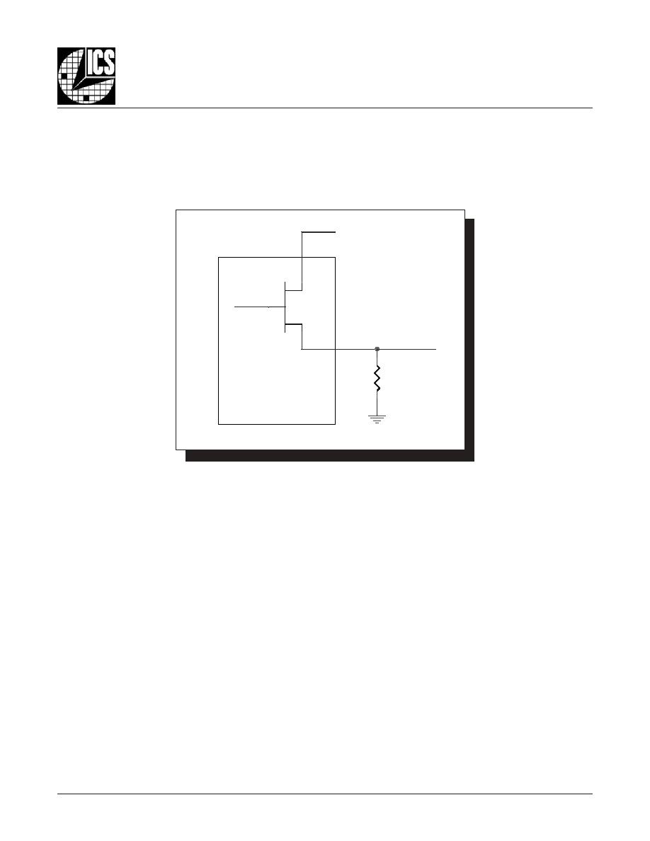
8427DY-02
www.icst.com/products/hiperclocks.html
REV. A FEBRUARY 17, 2006
16
Integrated
Circuit
Systems, Inc.
ICS8427-02
500MH
Z
, L
OW
J
ITTER
LVCMOS/C
RYSTAL
-
TO
-LVHSTL F
REQUENCY
S
YNTHESIZER
3. Calculations and Equations.
The purpose of this section is to derive the power dissipated into the load.
LVHSTL output driver circuit and termination are shown in
Figure 7.
T
o calculate worst case power dissipation into the load, use the following equations which assume a 50
load.
Pd_H is power dissipation when the output drives high.
Pd_L is the power dissipation when the output drives low.
Pd_H = (V
OH_MIN
/R
L
) * (V
DD_MAX
- V
OH_MIN
)
Pd_L = (V
OL_MAX
/R
L
) * (V
DD_MAX
- V
OL_MAX
)
Pd_H = (0.9V/50
) * (2V - 0.9V) = 19.8mW
Pd_L = (0.4V/50
) * (2V - 0.4V) = 12.8mW
Total Power Dissipation per output pair = Pd_H + Pd_L = 32.6mW
F
IGURE
7. LVHSTL D
RIVER
C
IRCUIT
AND
T
ERMINATION
V
DDO
V
OUT
RL
50
Q1

8427DY-02
www.icst.com/products/hiperclocks.html
REV. A FEBRUARY 17, 2006
17
Integrated
Circuit
Systems, Inc.
ICS8427-02
500MH
Z
, L
OW
J
ITTER
LVCMOS/C
RYSTAL
-
TO
-LVHSTL F
REQUENCY
S
YNTHESIZER
R
ELIABILITY
I
NFORMATION
T
RANSISTOR
C
OUNT
The transistor count for ICS8427-02 is: 4585
T
ABLE
9A.
JA
VS
. A
IR
F
LOW
T
ABLE
FOR
32 L
EAD
LQFP
JA
by Velocity (Linear Feet per Minute)
0
200
500
Single-Layer PCB, JEDEC Standard Test Boards
67.8�C/W
55.9�C/W
50.1�C/W
Multi-Layer PCB, JEDEC Standard Test Boards
47.9�C/W
42.1�C/W
39.4�C/W
NOTE: Most modern PCB designs use multi-layered boards. The data in the second row pertains to most designs.
T
ABLE
9B.
JA
VS
. A
IR
F
LOW
T
ABLE
FOR
A
32 L
EAD
VFQFN
JA
0 Air Flow (Linear Feet per Minute)
0
Multi-Layer PCB, JEDEC Standard Test Boards
34.8�C/W
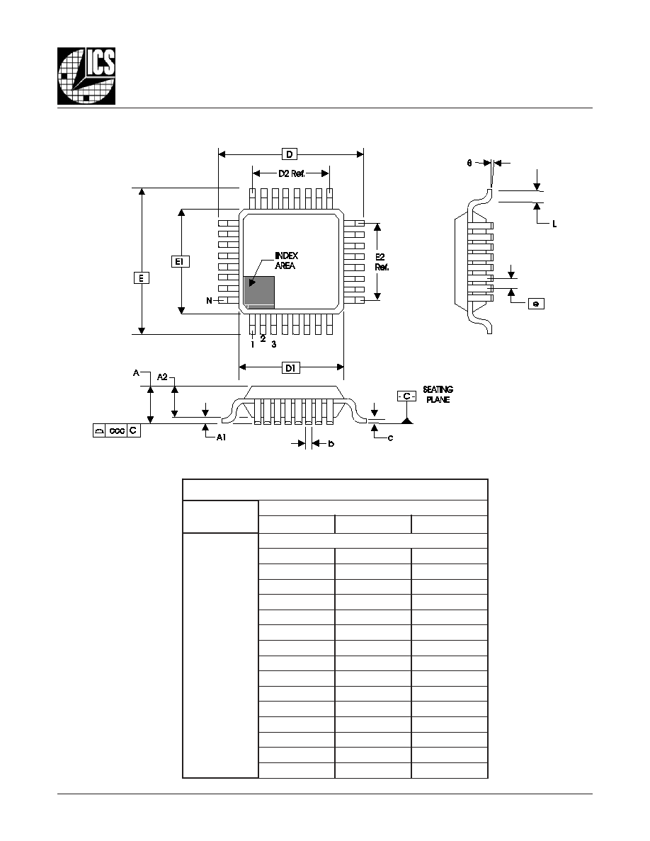
8427DY-02
www.icst.com/products/hiperclocks.html
REV. A FEBRUARY 17, 2006
18
Integrated
Circuit
Systems, Inc.
ICS8427-02
500MH
Z
, L
OW
J
ITTER
LVCMOS/C
RYSTAL
-
TO
-LVHSTL F
REQUENCY
S
YNTHESIZER
P
ACKAGE
O
UTLINE
- Y S
UFFIX
FOR
32 L
EAD
LQFP
T
ABLE
10A. P
ACKAGE
D
IMENSIONS
N
O
I
T
A
I
R
A
V
C
E
D
E
J
S
R
E
T
E
M
I
L
L
I
M
N
I
S
N
O
I
S
N
E
M
I
D
L
L
A
L
O
B
M
Y
S
A
B
B
M
U
M
I
N
I
M
L
A
N
I
M
O
N
M
U
M
I
X
A
M
N
2
3
A
0
6
.
1
1
A
5
0
.
0
5
1
.
0
2
A
5
3
.
1
0
4
.
1
5
4
.
1
b
0
3
.
0
7
3
.
0
5
4
.
0
c
9
0
.
0
0
2
.
0
D
C
I
S
A
B
0
0
.
9
1
D
C
I
S
A
B
0
0
.
7
2
D
0
6
.
5
E
C
I
S
A
B
0
0
.
9
1
E
C
I
S
A
B
0
0
.
7
2
E
0
6
.
5
e
C
I
S
A
B
0
8
.
0
L
5
4
.
0
0
6
.
0
5
7
.
0
q
�
0
�
7
c
c
c
0
1
.
0
Reference Document: JEDEC Publication 95, MS-026
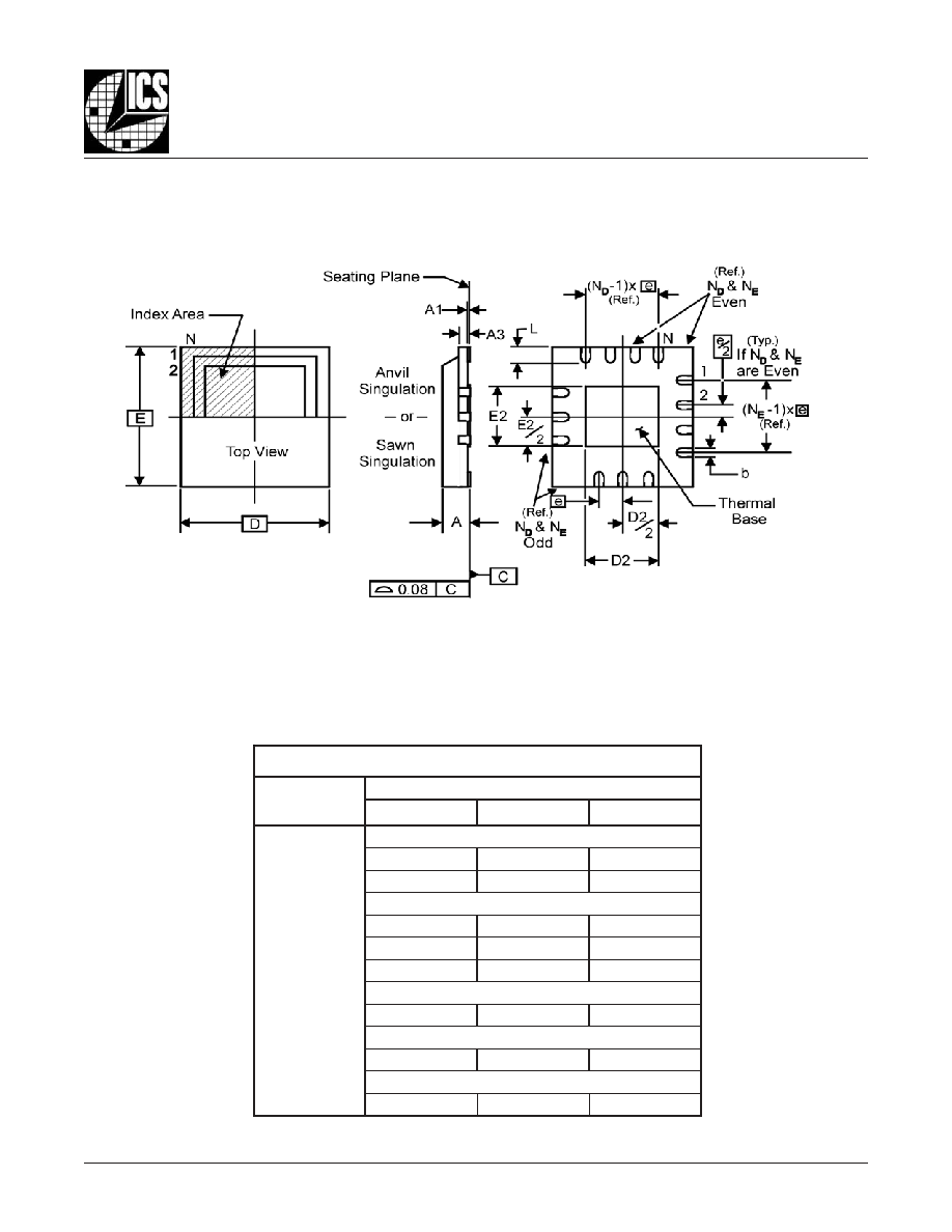
8427DY-02
www.icst.com/products/hiperclocks.html
REV. A FEBRUARY 17, 2006
19
Integrated
Circuit
Systems, Inc.
ICS8427-02
500MH
Z
, L
OW
J
ITTER
LVCMOS/C
RYSTAL
-
TO
-LVHSTL F
REQUENCY
S
YNTHESIZER
P
ACKAGE
O
UTLINE
- K S
UFFIX
FOR
A
32 L
EAD
VFQFN
T
ABLE
10B. P
ACKAGE
D
IMENSIONS
Reference Document: JEDEC Publication 95, MO-220
N
O
I
T
A
I
R
A
V
C
E
D
E
J
S
R
E
T
E
M
I
L
L
I
M
N
I
S
N
O
I
S
N
E
M
I
D
L
L
A
L
O
B
M
Y
S
2
-
D
H
H
V
M
U
M
I
N
I
M
L
A
N
I
M
O
N
M
U
M
I
X
A
M
N
2
3
A
0
8
.
0
-
-
0
0
.
1
1
A
0
-
-
5
0
.
0
3
A
.
f
e
R
5
2
.
0
b
8
1
.
0
5
2
.
0
0
3
.
0
N
D
8
N
E
8
D
C
I
S
A
B
0
0
.
5
2
D
5
2
.
1
5
2
.
2
5
2
.
3
E
C
I
S
A
B
0
0
.
5
2
E
5
2
.
1
5
2
.
2
5
2
.
3
e
C
I
S
A
B
0
5
.
0
L
0
3
.
0
0
4
.
0
0
5
.
0
8427DY-02
www.icst.com/products/hiperclocks.html
REV. A FEBRUARY 17, 2006
20
Integrated
Circuit
Systems, Inc.
ICS8427-02
500MH
Z
, L
OW
J
ITTER
LVCMOS/C
RYSTAL
-
TO
-LVHSTL F
REQUENCY
S
YNTHESIZER
T
ABLE
11. O
RDERING
I
NFORMATION
While the information presented herein has been checked for both accuracy and reliability, Integrated Circuit Systems, Incorporated (ICS) assumes no responsibility for either its use
or for infringement of any patents or other rights of third parties, which would result from its use. No other circuits, patents, or licenses are implied. This product is intended for use
in normal commercial applications. Any other applications such as those requiring extended temperature range, high reliability, or other extraordinary environmental requirements are
not recommended without additional processing by ICS. ICS reserves the right to change any circuitry or specifications without notice. ICS does not authorize or warrant any ICS
product for use in life support devices or critical medical instruments.
The aforementioned trademark, HiPerClockSTM is a trademark of Integrated Circuit Systems, Inc. or its subsidiaries in the United States and/or other countries.
r
e
b
m
u
N
r
e
d
r
O
/
t
r
a
P
g
n
i
k
r
a
M
e
g
a
k
c
a
P
g
n
i
g
a
k
c
a
P
g
n
i
p
p
i
h
S
e
r
u
t
a
r
e
p
m
e
T
2
0
-
Y
D
7
2
4
8
S
C
I
2
0
-
Y
D
7
2
4
8
S
C
I
P
F
Q
L
d
a
e
L
2
3
y
a
r
t
C
�
0
7
o
t
C
�
0
T
2
0
-
Y
D
7
2
4
8
S
C
I
2
0
-
Y
D
7
2
4
8
S
C
I
P
F
Q
L
d
a
e
L
2
3
l
e
e
r
&
e
p
a
t
0
0
0
1
C
�
0
7
o
t
C
�
0
F
L
2
0
-
Y
D
7
2
4
8
S
C
I
L
2
0
Y
D
7
2
4
8
S
C
I
P
F
Q
L
"
e
e
r
F
-
d
a
e
L
"
d
a
e
L
2
3
y
a
r
t
C
�
0
7
o
t
C
�
0
T
F
L
2
0
-
Y
D
7
2
4
8
S
C
I
L
2
0
Y
D
7
2
4
8
S
C
I
P
F
Q
L
"
e
e
r
F
-
d
a
e
L
"
d
a
e
L
2
3
l
e
e
r
&
e
p
a
t
0
0
0
1
C
�
0
7
o
t
C
�
0
2
0
-
K
D
7
2
4
8
S
C
I
2
0
-
K
D
7
2
4
8
S
C
I
N
F
Q
F
V
d
a
e
L
2
3
y
a
r
t
C
�
0
7
o
t
C
�
0
T
2
0
-
K
D
7
2
4
8
S
C
I
2
0
-
K
D
7
2
4
8
S
C
I
N
F
Q
F
V
d
a
e
L
2
3
l
e
e
r
&
e
p
a
t
0
0
5
2
C
�
0
7
o
t
C
�
0
F
L
2
0
-
K
D
7
2
4
8
S
C
I
D
B
T
N
F
Q
F
V
"
e
e
r
F
-
d
a
e
L
"
d
a
e
L
2
3
y
a
r
t
C
�
0
7
o
t
C
�
0
T
F
L
2
0
-
K
D
7
2
4
8
S
C
I
D
B
T
N
F
Q
F
V
"
e
e
r
F
-
d
a
e
L
"
d
a
e
L
2
3
l
e
e
r
&
e
p
a
t
0
0
5
2
C
�
0
7
o
t
C
�
0
.
t
n
a
il
p
m
o
c
S
H
o
R
e
r
a
d
n
a
n
o
i
t
a
r
u
g
i
f
n
o
c
e
e
r
F
-
b
P
e
h
t
e
r
a
r
e
b
m
u
n
t
r
a
p
e
h
t
o
t
x
i
f
f
u
s
"
F
L
"
n
a
h
t
i
w
d
e
r
e
d
r
o
e
r
a
t
a
h
t
s
t
r
a
P
:
E
T
O
N
8427DY-02
www.icst.com/products/hiperclocks.html
REV. A FEBRUARY 17, 2006
21
Integrated
Circuit
Systems, Inc.
ICS8427-02
500MH
Z
, L
OW
J
ITTER
LVCMOS/C
RYSTAL
-
TO
-LVHSTL F
REQUENCY
S
YNTHESIZER
T
E
E
H
S
Y
R
O
T
S
I
H
N
O
I
S
I
V
E
R
v
e
R
e
l
b
a
T
e
g
a
P
e
g
n
a
h
C
f
o
n
o
i
t
p
i
r
c
s
e
D
e
t
a
D
A
1
1
T
0
1
0
2
.
m
a
r
g
a
i
d
t
i
u
c
r
i
C
t
s
e
T
C
A
d
a
o
L
t
u
p
t
u
O
d
e
t
a
d
p
U
.
e
g
a
k
c
a
p
P
F
Q
L
r
o
f
g
n
i
k
r
a
m
e
e
r
f
-
d
a
e
l
d
e
d
d
a
-
e
l
b
a
T
n
o
i
t
a
m
r
o
f
n
I
g
n
i
r
e
d
r
O
6
0
/
7
1
/
2