Document Outline
- General Description
- Features
- Frequency Select Function Table
- Pin Assignment
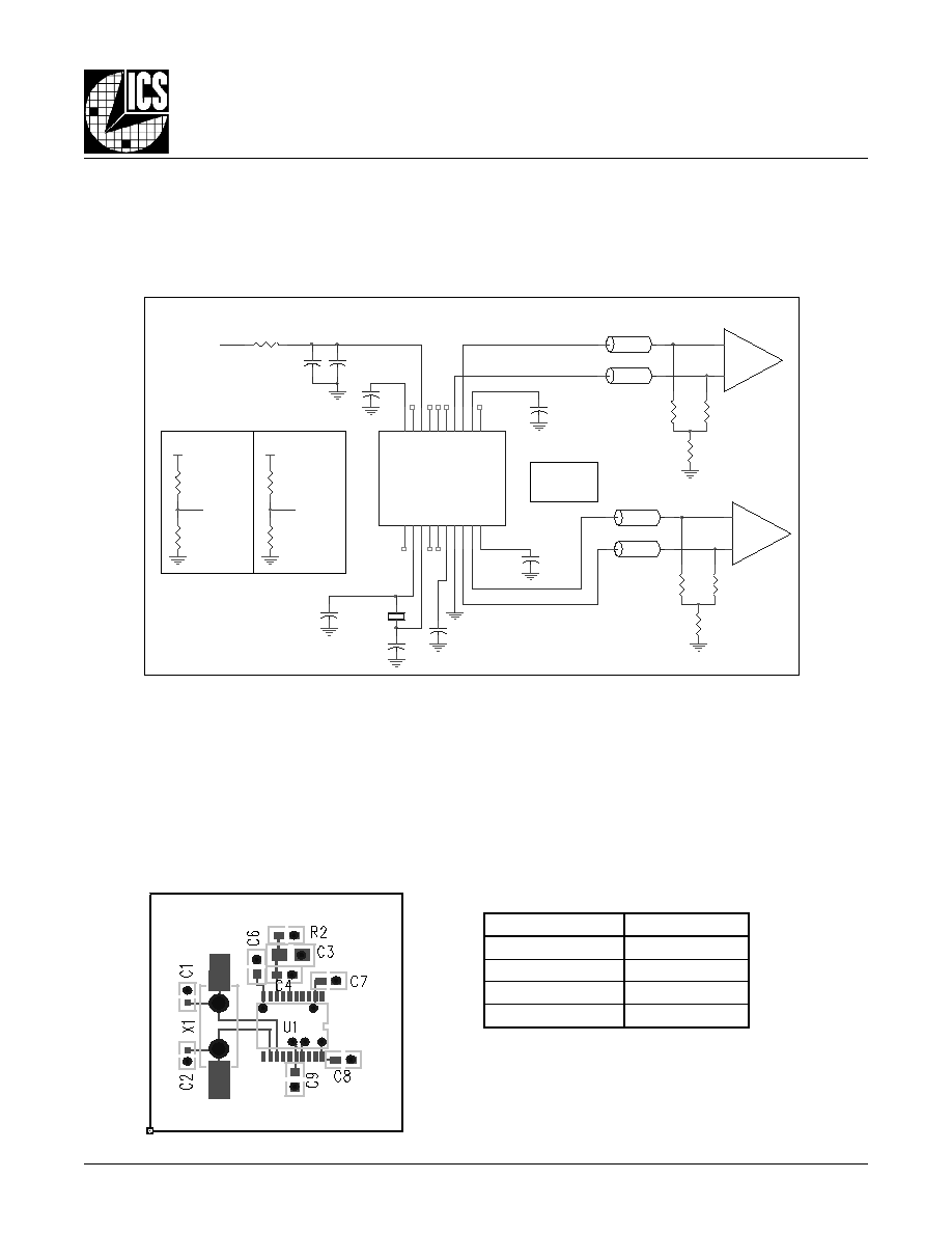
- Block Diagram
- Pin Descriptions
- Pin Characteristics
- Absolute Maximum Ratings
- Power Supply DC Characteristics
- LVCMOS DC Characteristics
- LVPECL DC Characteristics
- Crystal Characteristics
- AC Characteristics
- Typical Phase Noise at 53.125MHz
- Typical Phase Noise at 106.25MHz
- Typical Phase Noise at 159.375MHz
- Typical Phase Noise at 212.5MHz
- Parameter Measurement Information
- 3.3V Core/3.3V Output Load AC Test Circuit Diagram
- Output Skew Diagram
- RMS Phase Jitter Diagram
- Propagation Delay Diagram
- Output Duty Cycle Pulse Width/Period Diagram
- Output Rise/Fall Time Diagram
- Application Information
- Power Supply Filtering Techniques
- Termination for 3.3V LVPECL Output
- Crystal Input Interface
- Layout Guideline
- Schematic Example
- PC Board Layout Example
- Footprint Table
- Power Considerations
- Power Dissipation
- Junction Temperature
- Thermal Resistance
- Calculations & Equations
- LVPECL Driver Circuit & Termination
- Reliability Information
- Transistor Count
- Package Outline
- Package Dimensions
- Ordering Information
- Revision History Sheet
843002AG
www.icst.com/products/hiperclocks.html
REV. B MAY 6, 2005
1
Integrated
Circuit
Systems, Inc.
ICS843002
F
EMTO
C
LOCKS
TM C
RYSTAL
-
TO
-
3.3V LVPECL F
REQUENCY
S
YNTHESIZER
G
ENERAL
D
ESCRIPTION
The ICS843002 is a 2 output LVPECL synthesizer
optimized to generate Fibre Channel reference
clock frequencies and is a member of the
HiPerClocks
TM
family of high performance clock
solutions from ICS. Using a 26.5625MHz, 18pF
parallel resonant crystal, the following frequencies can be
generated based on the 2 frequency select pins (F_SEL[1:0]):
212.5MHz, 187.5MHz, 159.375MHz, 106.25MHz, and
53.125MHz. The ICS843002 uses ICS' 3
rd
generation low
phase noise VCO technology and can achieve 1ps or lower
typical rms phase jitter, easily meeting Fibre Channel jitter
requirements. The ICS843002 is packaged in a small 20-pin
TSSOP package.
F
EATURES
� Two 3.3V LVPECL outputs
� Selectable crystal oscillator interface
or LVCMOS/LVTTL single-ended input
� Supports the following output frequencies: 212.5MHz,
187.5MHz, 159.375MHz, 106.25MHz and 53.125MHz
� VCO range: 560MHz - 680MHz
� RMS phase jitter (637kHz - 10MHz): 0.72ps (typical)
� Typical phase noise at 212.5MHz
Phase noise:
Offset
Noise Power
100Hz ............... -87.7 dBc/Hz
1KHz .............. -111.6 dBc/Hz
10KHz .............. -124.3 dBc/Hz
100KHz .............. -124.3 dBc/Hz
� Full 3.3V supply mode
� Lead-Free package RoHS compliant
� -30�C to 85�C ambient operating temperature
HiPerClockSTM
ICS
P
IN
A
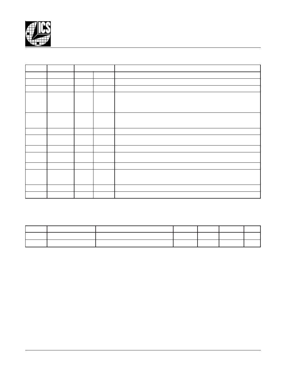
SSIGNMENT
1
1
0
1
0
Phase
Detector
VCO
637.5MHz
(w/26.5625MHz
Reference)
OSC
M = 24 (fixed)
F_SEL[1:0]
0 0 �3
0 1 �4
1 0 �6
1 1 �12
2
ICS843002
20-Lead TSSOP
6.5mm x 4.4mm x 0.92mm
package body
G Package
Top View
B
LOCK
D
IAGRAM
F
REQUENCY
S
ELECT
F
UNCTION
T
ABLE
F_SEL[1:0]
nPLL_SEL
TEST_CLK
XTAL_IN
XTAL_OUT
nXTAL_SEL
MR
Q0
nQ0
Q1
nQ1
Pulldown
Pulldown
26.5625MHz
nc
V
CCO
Q0
nQ0
MR
nPLL_SEL
nc
V
CCA
F_SEL0
V
CC
1
2
3
4
5
6
7
8
9
10
20
19
18
17
16
15
14
13
12
11
V
CCO
Q1
nQ1
V
EE
V
CC
nXTAL_SEL
TEST_CLK
XTAL_IN
XTAL_OUT
F_SEL1
Pulldown
Pulldown
Pulldown
s
t
u
p
n
I
t
u
p
t
u
O
y
c
n
e
u
q
e
r
F
)
z
H
M
(
t
u
p
n
I
y
c
n
e
u
q
e
r
F
)
z
H
M
(
1
L
E
S
_
F
0
L
E
S
_
F
r
e
d
i
v
i
D
M
e
u
l
a
V
r
e
d
i
v
i
D
N
e
u
l
a
V
N
/
M
e
u
l
a
V
r
e
d
i
v
i
D
5
2
6
5
.
6
2
0
0
4
2
3
8
5
.
2
1
2
5
2
6
5
.
6
2
0
1
4
2
4
6
5
7
3
.
9
5
1
5
2
6
5
.
6
2
1
0
4
2
6
4
5
2
.
6
0
1
5
2
6
5
.
6
2
1
1
4
2
2
1
2
5
2
1
.
3
5
5
7
3
4
.
3
2
0
0
4
2
3
8
5
.
7
8
1
843002AG
www.icst.com/products/hiperclocks.html
REV. B MAY 6, 2005
2
Integrated
Circuit
Systems, Inc.
ICS843002
F
EMTO
C
LOCKS
TM C
RYSTAL
-
TO
-
3.3V LVPECL F
REQUENCY
S
YNTHESIZER
T
ABLE
1. P
IN
D
ESCRIPTIONS
T
ABLE
2. P
IN
C
HARACTERISTICS
r
e
b
m
u
N
e
m
a
N
e
p
y
T
n
o
i
t
p
i
r
c
s
e
D
7
,
1
c
n
d
e
s
u
n
U
.
t
c
e
n
n
o
c
o
N
0
2
,
2
V
O
C
C
r
e
w
o
P
.
s
n
i
p
y
l
p
p
u
s
t
u
p
t
u
O
4
,
3
0
Q
n
,
0
Q
t
u
p
u
O
.
s
l
e
v
e
l
e
c
a
f
r
e
t
n
i
L
C
E
P
V
L
.
r
i
a
p
t
u
p
t
u
o
l
a
i
t
n
e
r
e
f
f
i
D
5
R
M
t
u
p
n
I
n
w
o
d
ll
u
P
e
r
a
s
r
e
d
i
v
i
d
l
a
n
r
e
t
n
i
e
h
t
,
H
G
I
H
c
i
g
o
l
n
e
h
W
.
t
e
s
e
R
r
e
t
s
a
M
H
G
I
H
e
v
i
t
c
A
x
Q
n
s
t
u
p
t
u
o
d
e
t
r
e
v
n
i
e
h
t
d
n
a
w
o
l
o
g
o
t
x
Q
s
t
u
p
t
u
o
e
u
r
t
e
h
t
g
n
i
s
u
a
c
t
e
s
e
r
e
r
a
s
t
u
p
t
u
o
e
h
t
d
n
a
s
r
e
d
i
v
i
d
l
a
n
r
e
t
n
i
e
h
t
,
W
O
L
c
i
g
o
l
n
e
h
W
.
h
g
i
h
o
g
o
t
.
s
l
e
v
e
l
e
c
a
f
r
e
t
n
i
L
T
T
V
L
/
S
O
M
C
V
L
.
d
e
l
b
a
n
e
6
L
E
S
_
L
L
P
n
t
u
p
n
I
n
w
o
d
ll
u
P
n
e
h
W
.
s
r
e
d
i
v
i
d
e
h
t
o
t
t
u
p
n
i
s
a
K
L
C
_
T
S
E
T
d
n
a
L
L
P
e
h
t
n
e
e
w
t
e
b
s
t
c
e
l
e
S
k
c
o
l
c
e
c
n
e
r
e
f
e
r
e
h
t
s
t
c
e
l
e
s
e
d
,
H
G
I
H
n
e
h
W
.
)
e
l
b
a
n
E
L
L
P
(
L
L
P
s
t
c
e
l
e
s
,
W
O
L
.
s
l
e
v
e
l
e
c
a
f
r
e
t
n
i
L
T
T
V
L
/
S
O
M
C
V
L
.
)
s
s
a
p
y
B
L
L
P
(
8
V
A
C
C
r
e
w
o
P
.
n
i
p
y
l
p
p
u
s
g
o
l
a
n
A
1
1
,
9
,
0
L
E
S
_
F
1
L
E
S
_
F
t
u
p
n
I
n
w
o
d
ll
u
P
.
s
l
e
v
e
l
e
c
a
f
r
e
t
n
i
L
T
T
V
L
/
S
O
M
C
V
L
.
s
n
i
p
t
c
e
l
e
s
y
c
n
e
u
q
e
r
F
6
1
,
0
1
V
C
C
r
e
w
o
P
.
n
i
p
y
l
p
p
u
s
e
r
o
C
3
1
,
2
1
,
T
U
O
_
L
A
T
X
N
I
_
L
A
T
X
t
u
p
n
I
,
t
u
p
t
u
o
e
h
t
s
i
T
U
O
_
L
A
T
X
.
e
c
a
f
r
e
t
n
i
l
a
t
s
y
r
c
t
n
a
n
o
s
e
r
l
e
ll
a
r
a
P
.
t
u
p
n
i
e
h
t
s
i
N
I
_
L
A
T
X
4
1
K
L
C
_
T
S
E
T
t
u
p
n
I
n
w
o
d
ll
u
P
.
t
u
p
n
i
k
c
o
l
c
L
T
T
V
L
/
S
O
M
C
V
L
5
1
L
E
S
_
L
A
T
X
n
t
u
p
n
I
n
w
o
d
ll
u
P
e
c
n
e
r
e
f
e
R
L
L
P
e
h
t
e
h
t
s
a
s
t
u
p
n
i
K
L
C
_
T
S
E
T
r
o
l
a
t
s
y
r
c
n
e
e
w
t
e
b
s
t
c
e
l
e
S
.
H
G
I
H
n
e
h
w
K
L
C
_
T
S
E
T
s
t
c
e
l
e
S
.
W
O
L
n
e
h
w
s
t
u
p
n
i
L
A
T
X
s
t
c
e
l
e
S
.
e
c
r
u
o
s
.
s
l
e
v
e
l
e
c
a
f
r
e
t
n
i
L
T
T
V
L
/
S
O
M
C
V
L
7
1
V
E
E
r
e
w
o
P
.
s
n
i
p
y
l
p
p
u
s
e
v
i
t
a
g
e
N
9
1
,
8
1
1
Q
,
1
Q
n
t
u
p
t
u
O
.
s
l
e
v
e
l
e
c
a
f
r
e
t
n
i
L
C
E
P
V
L
.
r
i
a
p
t
u
p
t
u
o
l
a
i
t
n
e
r
e
f
f
i
D
:
E
T
O
N
n
w
o
d
ll
u
P
.
s
e
u
l
a
v
l
a
c
i
p
y
t
r
o
f
,
s
c
i
t
s
i
r
e
t
c
a
r
a
h
C
n
i
P
,
2
e
l
b
a
T
e
e
S
.
s
r
o
t
s
i
s
e
r
t
u
p
n
i
l
a
n
r
e
t
n
i
o
t
r
e
f
e
r
l
o
b
m
y
S
r
e
t
e
m
a
r
a
P
s
n
o
i
t
i
d
n
o
C
t
s
e
T
m
u
m
i
n
i
M
l
a
c
i
p
y
T
m
u
m
i
x
a
M
s
t
i
n
U
C
N
I
e
c
n
a
t
i
c
a
p
a
C
t
u
p
n
I
4
F
p
R
N
W
O
D
L
L
U
P
r
o
t
s
i
s
e
R
n
w
o
d
ll
u
P
t
u
p
n
I
1
5
k
843002AG
www.icst.com/products/hiperclocks.html
REV. B MAY 6, 2005
3
Integrated
Circuit
Systems, Inc.
ICS843002
F
EMTO
C
LOCKS
TM C
RYSTAL
-
TO
-
3.3V LVPECL F
REQUENCY
S
YNTHESIZER
T
ABLE
3A. P
OWER
S
UPPLY
DC C
HARACTERISTICS
,
V
CC
= V
CCA
= V
CCO
= 3.3V�10%, TA = -30�C
TO
85�C
T
ABLE
3B. LVCMOS / LVTTL DC C
HARACTERISTICS
,
V
CC
= V
CCA
= V
CCO
= 3.3V�10%, TA = -30�C
TO
85�C
A
BSOLUTE
M
AXIMUM
R
ATINGS
Supply Voltage, V
CC
4.6V
Inputs, V
I
-0.5V to V
CC
+ 0.5V
Outputs, I
O
Continuous Current
50mA
Surge Current
100mA
Package Thermal Impedance,
JA
73.2�C/W (0 lfpm)
Storage Temperature, T
STG
-65�C to 150�C
NOTE: Stresses beyond those listed under Absolute
Maximum Ratings may cause permanent damage to the
device. These ratings are stress specifications only. Functional
operation of product at these conditions or any conditions be-
yond those listed in the
DC Characteristics or AC Character-
istics is not implied. Exposure to absolute maximum rating
conditions for extended periods may affect product reliability.
l
o
b
m
y
S
r
e
t
e
m
a
r
a
P
s
n
o
i
t
i
d
n
o
C
t
s
e
T
m
u
m
i
n
i
M
l
a
c
i
p
y
T
m
u
m
i
x
a
M
s
t
i
n
U
V
H
I
e
g
a
t
l
o
V
h
g
i
H
t
u
p
n
I
2
V
C
C
3
.
0
+
V
V
L
I
t
u
p
n
I
e
g
a
t
l
o
V
w
o
L
,
L
E
S
_
L
A
T
X
n
,
L
E
S
_
L
L
P
n
R
M
,
1
L
E
S
_
F
,
0
L
E
S
_
F
3
.
0
-
8
.
0
V
K
L
C
_
T
S
E
T
3
.
0
-
0
.
1
V
I
H
I
t
u
p
n
I
t
n
e
r
r
u
C
h
g
i
H
,
R
M
,
K
L
C
_
T
S
E
T
,
1
L
E
S
_
F
,
0
L
E
S
_
F
,
L
E
S
_
L
A
T
X
n
,
L
E
S
_
L
L
P
n
V
C
C
V
=
N
I
V
3
6
.
3
=
0
5
1
A
�
I
L
I
t
u
p
n
I
t
n
e
r
r
u
C
w
o
L
,
R
M
,
K
L
C
_
T
S
E
T
,
1
L
E
S
_
F
,
0
L
E
S
_
F
,
L
E
S
_
L
A
T
X
n
,
L
E
S
_
L
L
P
n
V
C
C
V
,
V
3
6
.
3
=
N
I
V
0
=
0
5
1
-
A
�
l
o
b
m
y
S
r
e
t
e
m
a
r
a
P
s
n
o
i
t
i
d
n
o
C
t
s
e
T
m
u
m
i
n
i
M
l
a
c
i
p
y
T
m
u
m
i
x
a
M
s
t
i
n
U
V
C
C
e
g
a
t
l
o
V
y
l
p
p
u
S
e
r
o
C
7
9
.
2
3
.
3
3
6
.
3
V
V
A
C
C
e
g
a
t
l
o
V
y
l
p
p
u
S
g
o
l
a
n
A
7
9
.
2
3
.
3
3
6
.
3
V
V
O
C
C
e
g
a
t
l
o
V
y
l
p
p
u
S
t
u
p
t
u
O
7
9
.
2
3
.
3
3
6
.
3
V
I
E
E
t
n
e
r
r
u
C
y
l
p
p
u
S
r
e
w
o
P
5
3
1
A
m
I
C
C
t
n
e
r
r
u
C
y
l
p
p
u
S
e
r
o
C
0
0
1
A
m
I
A
C
C
t
n
e
r
r
u
C
y
l
p
p
u
S
g
o
l
a
n
A
5
1
A
m
I
O
C
C
t
n
e
r
r
u
C
y
l
p
p
u
S
t
u
p
t
u
O
1
3
A
m
T
ABLE
3C. LVPECL DC C
HARACTERISTICS
,
V
CC
= V
CCA
= V
CCO
= 3.3V�10%, TA = -30�C
TO
85�C
l
o
b
m
y
S
r
e
t
e
m
a
r
a
P
s
n
o
i
t
i
d
n
o
C
t
s
e
T
m
u
m
i
n
i
M
l
a
c
i
p
y
T
m
u
m
i
x
a
M
s
t
i
n
U
V
H
O
1
E
T
O
N
;
e
g
a
t
l
o
V
h
g
i
H
t
u
p
t
u
O
V
O
C
C
4
.
1
-
V
O
C
C
9
.
0
-
V
V
L
O
1
E
T
O
N
;
e
g
a
t
l
o
V
w
o
L
t
u
p
t
u
O
V
O
C
C
0
.
2
-
V
O
C
C
7
.
1
-
V
V
G
N
I
W
S
g
n
i
w
S
e
g
a
t
l
o
V
t
u
p
t
u
O
k
a
e
P
-
o
t
-
k
a
e
P
6
.
0
0
.
1
V
0
5
h
t
i
w
d
e
t
a
n
i
m
r
e
t
s
t
u
p
t
u
O
:
1
E
T
O
N
V
o
t
O
C
C
.
V
2
-
843002AG
www.icst.com/products/hiperclocks.html
REV. B MAY 6, 2005
4
Integrated
Circuit
Systems, Inc.
ICS843002
F
EMTO
C
LOCKS
TM C
RYSTAL
-
TO
-
3.3V LVPECL F
REQUENCY
S
YNTHESIZER
T
ABLE
5. AC C
HARACTERISTICS
,
V
CC
= V
CCA
= V
CCO
= 3.3V�10%, TA = -30�C
TO
85�C
T
ABLE
4. C
RYSTAL
C
HARACTERISTICS
r
e
t
e
m
a
r
a
P
s
n
o
i
t
i
d
n
o
C
t
s
e
T
m
u
m
i
n
i
M
l
a
c
i
p
y
T
m
u
m
i
x
a
M
s
t
i
n
U
n
o
i
t
a
ll
i
c
s
O
f
o
e
d
o
M
l
a
t
n
e
m
a
d
n
u
F
y
c
n
e
u
q
e
r
F
3
3
.
3
2
5
2
6
5
.
6
2
3
3
.
8
2
z
H
M
)
R
S
E
(
e
c
n
a
t
s
i
s
e
R
s
e
i
r
e
S
t
n
e
l
a
v
i
u
q
E
0
5
e
c
n
a
t
i
c
a
p
a
C
t
n
u
h
S
7
F
p
.
l
a
t
s
y
r
c
t
n
a
n
o
s
e
r
l
e
ll
a
r
a
p
F
p
8
1
n
a
g
n
i
s
u
d
e
z
i
r
e
t
c
a
r
a
h
C
:
E
T
O
N
l
o
b
m
y
S
r
e
t
e
m
a
r
a
P
s
n
o
i
t
i
d
n
o
C
t
s
e
T
m
u
m
i
n
i
M
l
a
c
i
p
y
T
m
u
m
i
x
a
M
s
t
i
n
U
f
T
U
O
y
c
n
e
u
q
e
r
F
t
u
p
t
u
O
0
0
=
]
0
:
1
[
L
E
S
_
F
7
6
.
6
8
1
7
6
.
6
2
2
z
H
M
1
0
=
]
0
:
1
[
L
E
S
_
F
0
4
1
0
7
1
z
H
M
0
1
=
]
0
:
1
[
L
E
S
_
F
3
3
.
3
9
3
3
.
3
1
1
z
H
M
1
1
=
]
0
:
1
[
L
E
S
_
F
7
6
.
6
4
7
6
.
6
5
z
H
M
t
)
o
(
k
s
2
,
1
E
T
O
N
;
w
e
k
S
t
u
p
t
u
O
0
2
s
p
t
)
�
(
t
ij
;
)
m
o
d
n
a
R
(
r
e
t
t
i
J
e
s
a
h
P
S
M
R
3
E
T
O
N
)
z
H
M
0
1
-
z
H
K
7
3
6
(
,
z
H
M
5
.
2
1
2
2
7
.
0
s
p
)
z
H
M
0
1
-
z
H
K
7
3
6
(
,
z
H
M
5
7
3
.
9
5
1
6
7
.
0
s
p
)
z
H
M
0
1
-
z
H
K
7
3
6
(
,
z
H
M
5
2
.
6
0
1
4
8
.
0
s
p
)
z
H
M
0
1
-
z
H
K
7
3
6
(
,
z
H
M
5
2
1
.
3
5
7
9
.
0
s
p
t
R
t
/
F
e
m
i
T
ll
a
F
/
e
s
i
R
t
u
p
t
u
O
%
0
8
o
t
%
0
2
0
0
3
0
0
6
s
p
c
d
o
e
l
c
y
C
y
t
u
D
t
u
p
t
u
O
0
0
=
]
0
:
1
[
L
E
S
_
F
6
4
4
5
%
]
0
:
1
[
L
E
S
_
F
0
0
9
4
1
5
%
.
s
n
o
i
t
i
d
n
o
c
d
a
o
l
l
a
u
q
e
h
t
i
w
d
n
a
s
e
g
a
t
l
o
v
y
l
p
p
u
s
e
m
a
s
e
h
t
t
a
s
t
u
p
t
u
o
n
e
e
w
t
e
b
w
e
k
s
s
a
d
e
n
i
f
e
D
:
1
E
T
O
N
V
t
a
d
e
r
u
s
a
e
M
O
C
C
.
2
/
.
5
6
d
r
a
d
n
a
t
S
C
E
D
E
J
h
t
i
w
e
c
n
a
d
r
o
c
c
a
n
i
d
e
n
i
f
e
d
s
i
r
e
t
e
m
a
r
a
p
s
i
h
T
:
2
E
T
O
N
.
t
o
l
p
e
s
i
o
N
e
s
a
h
P
e
e
S
:
3
E
T
O
N
843002AG
www.icst.com/products/hiperclocks.html
REV. B MAY 6, 2005
5
Integrated
Circuit
Systems, Inc.
ICS843002
F
EMTO
C
LOCKS
TM C
RYSTAL
-
TO
-
3.3V LVPECL F
REQUENCY
S
YNTHESIZER
106.25MHz
RMS Phase Jitter (Random)
637Khz to 10MHz = 0.84ps (typical)
O
FFSET
F
REQUENCY
(H
Z
)
0
-10
-20
-30
-40
-50
-60
-70
-80
-90
-100
-110
-120
-130
-140
-150
-160
-170
-180
-190
10
100
1k
10k
100k
1M
10M
100M
Fibre Channel Jitter Filter
Phase Noise Result by adding
Fibre Channel Filter to raw data
Raw Phase Noise Data
dBc
Hz
N
OISE
P
O
WER
T
YPICAL
P
HASE
N
OISE
AT
106.25MH
Z
T
YPICAL
P
HASE
N
OISE
AT
53.125MH
Z
0
-10
-20
-30
-40
-50
-60
-70
-80
-90
-100
-110
-120
-130
-140
-150
-160
-170
-180
-190
53.125MHz
RMS Phase Jitter (Random)
637Khz to 10MHz = 0.97ps (typical)
O
FFSET
F
REQUENCY
(H
Z
)
10
100
1k
10k
100k
1M
10M
100M
Fibre Channel Jitter Filter
Phase Noise Result by adding
Fibre Channel Filter to raw data
Raw Phase Noise Data
dBc
Hz
N
OISE
P
O
WER
843002AG
www.icst.com/products/hiperclocks.html
REV. B MAY 6, 2005
6
Integrated
Circuit
Systems, Inc.
ICS843002
F
EMTO
C
LOCKS
TM C
RYSTAL
-
TO
-
3.3V LVPECL F
REQUENCY
S
YNTHESIZER
T
YPICAL
P
HASE
N
OISE
AT
212.5MH
Z
212.5MHz
RMS Phase Jitter (Random)
637Khz to 10MHz = 0.72ps (typical)
O
FFSET
F
REQUENCY
(H
Z
)
0
-10
-20
-30
-40
-50
-60
-70
-80
-90
-100
-110
-120
-130
-140
-150
-160
-170
-180
-190
10
100
1k
10k
100k
1M
10M
100M
Fibre Channel Jitter Filter
Phase Noise Result by adding
Fibre Channel Filter to raw data
Raw Phase Noise Data
dBc
Hz
N
OISE
P
O
WER
0
-10
-20
-30
-40
-50
-60
-70
-80
-90
-100
-110
-120
-130
-140
-150
-160
-170
-180
-190
10
100
1k
10k
100k
1M
10M
100M
159.375MHz
RMS Phase Jitter (Random)
637Khz to 10MHz = 0.76ps (typical)
O
FFSET
F
REQUENCY
(H
Z
)
dBc
Hz
Fibre Channel Jitter Filter
Phase Noise Result by adding
Fibre Channel Filter to raw data
Raw Phase Noise Data
N
OISE
P
O
WER
T
YPICAL
P
HASE
N
OISE
AT
159.375MH
Z

843002AG
www.icst.com/products/hiperclocks.html
REV. B MAY 6, 2005
7
Integrated
Circuit
Systems, Inc.
ICS843002
F
EMTO
C
LOCKS
TM C
RYSTAL
-
TO
-
3.3V LVPECL F
REQUENCY
S
YNTHESIZER
P
ARAMETER
M
EASUREMENT
I
NFORMATION
t
PW
t
PERIOD
t
PW
t
PERIOD
odc =
x 100%
Q0, Q1
RMS P
HASE
J
ITTER
O
UTPUT
S
KEW
3.3V C
ORE
/3.3V O
UTPUT
L
OAD
AC T
EST
C
IRCUIT
SCOPE
Qx
nQx
LVPECL
2V
-1.3V � 0.33V
O
UTPUT
R
ISE
/F
ALL
T
IME
Clock
Outputs
20%
80%
80%
20%
t
R
t
F
V
SW I N G
V
CC
,
V
CCA
, V
CCO
V
EE
nQ0, nQ1
O
UTPUT
D
UTY
C
YCLE
/P
ULSE
W
IDTH
/P
ERIOD
tsk(o)
Qy
Qx
nQy
nQx
Phase Noise Mask
Offset Frequency
f
1
f
2
Phase Noise Plot
RMS Jitter = Area Under the Masked Phase Noise Plot
Noise P
o
w
er
843002AG
www.icst.com/products/hiperclocks.html
REV. B MAY 6, 2005
8
Integrated
Circuit
Systems, Inc.
ICS843002
F
EMTO
C
LOCKS
TM C
RYSTAL
-
TO
-
3.3V LVPECL F
REQUENCY
S
YNTHESIZER
A
PPLICATION
I
NFORMATION
As in any high speed analog circuitry, the power supply pins
are vulnerable to random noise. The ICS843002 provides
separate power supplies to isolate any high switching
noise from the outputs to the internal PLL. V
CC
, V
CCA
, and V
CCO
should be individually connected to the power supply
plane through vias, and bypass capacitors should be
used for each pin. To achieve optimum jitter performance,
power supply isolation is required.
Figure 1 illustrates how
a 10
resistor along with a 10�F and a .01F bypass
capacitor should be connected to each V
CCA
.
P
OWER
S
UPPLY
F
ILTERING
T
ECHNIQUES
F
IGURE
1. P
OWER
S
UPPLY
F
ILTERING
10
V
CCA
10
F
.01
F
3.3V
.01
F
V
CC
T
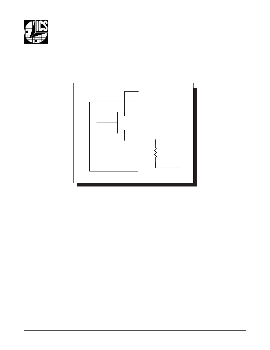
ERMINATION
FOR
3.3V LVPECL O
UTPUT
V
CC
- 2V
50
50
RTT
Z
o
= 50
Z
o
= 50
FOUT
FIN
RTT =
Z
o
1
((V
OH
+ V
OL
) / (V
CC
� 2)) � 2
3.3V
125
125
84
84
Z
o
= 50
Z
o
= 50
FOUT
FIN
The clock layout topology shown below is a typical termi-
nation for LVPECL outputs. The two different layouts men-
tioned are recommended only as guidelines.
FOUT and nFOUT are low impedance follower outputs that
generate ECL/LVPECL compatible outputs. Therefore, ter-
minating resistors (DC current path to ground) or current
sources must be used for functionality. These outputs are
F
IGURE
2B. LVPECL O
UTPUT
T
ERMINATION
F
IGURE
2A. LVPECL O
UTPUT
T
ERMINATION
designed to drive 50
transmission lines. Matched imped-
ance techniques should be used to maximize operating
frequency and minimize signal distortion.
Figures 2A and
2B show two different layouts which are recommended
only as guidelines. Other suitable clock layouts may exist
and it would be recommended that the board designers
simulate to guarantee compatibility across all printed cir-
cuit and clock component process variations.
843002AG
www.icst.com/products/hiperclocks.html
REV. B MAY 6, 2005
9
Integrated
Circuit
Systems, Inc.
ICS843002
F
EMTO
C
LOCKS
TM C
RYSTAL
-
TO
-
3.3V LVPECL F
REQUENCY
S
YNTHESIZER
C
RYSTAL
I
NPUT
I
NTERFACE
The ICS843002 has been characterized with 18pF parallel
resonant crystals. The capacitor values shown in
Figure 3
Figure 3. C
RYSTAL
I
NPU
t I
NTERFACE
below were determined using a 26.5625MHz 18pF parallel
resonant crystal and were chosen to minimize the ppm error.
ICS843002
C1
33p
X1
18pF Parallel Crystal
C2
27p
XTAL_OUT
XTAL_IN
843002AG
www.icst.com/products/hiperclocks.html
REV.
B MAY 6
, 2005
10
Integrated
Circuit
Systems, Inc.
ICS843002
F
EMTO
C
LOCKS
TM C
RYSTAL
-
TO
-
3.3V LVPECL F
REQUENCY
S
YNTHESIZER
L
AYOUT
G
UIDELINE
Figure 4A shows a schematic example of the ICS843002. An
example of LVEPCL termination is shown in this schematic.
Additional LVPECL termination approaches are shown in the
LVPECL Termination Application Note. In this example, an 18 pF
F
IGURE
4A. ICS843002 S
CHEMATIC
E
XAMPLE
parallel resonant 26.5625MHz crystal is used. The C1=27pF
and C2=33pF are recommended for frequency accuracy. For
different board layout, the C1 and C2 may be slightly adjusted
for optimizing frequency accuracy.
F
IGURE
4B. ICS843002 PC B
OARD
L
AYOUT
E
XAMPLE
C1
27pF
VCC
VCCO
Zo = 50 Ohm
R6
50
C6
0.1u
C4
0.01u
VC
C
X1
26.5625 MHz
VCC=3.3V
18pF
To Logic
Input
pins
C7
0.1u
Zo = 50 Ohm
RU1
1K
To Logic
Input
pins
C9
0.1u
Set Logic
Input to
'1'
VCCO=3.3V
VCC
VCC
R5
50
U1
ICS843002
2
3
4
5
6
7
8
9
10
11
12
13
14
15
16
17
18
19
20
1
VC
C
O
Q0
nQ0
MR
nP
LL_S
E
L
nc
VC
C
A
F_
S
E
L
0
VC
C
F
_
SEL
1
X
T
A
L_OU
T
X
T
A
L_I
N
T
E
S
T
_C
LK
nX
T
A
L_S
E
L
VC
C
VE
E
nQ1
Q1
VC
C
O
n
c
VCC
VCCO
RD2
1K
VCCA
R4
50
C3
10uF
Zo = 50 Ohm
RD1
Not Install
R2
10
Set Logic
Input to
'0'
Zo = 50 Ohm
+
-
C8
0.1u
R7
50
Logic Control Input Examples
R9
50
C2
33pF
R8
50
+
-
RU2
Not Install
PC B
OARD
L
AYOUT
E
XAMPLE
Figure 4B shows an example of ICS843002 P.C. board layout.
The crystal X1 footprint shown in this example allows installa-
tion of either surface mount HC49S or through-hole HC49 pack-
age. The footprints of other components in this example are listed
in the
Table 6. There should be at least one decoupling capacitor
per power pin. The decoupling capacitors should be located as
close as possible to the power pins. The layout assumes that
the board has clean analog power ground plane.
T
ABLE
6. F
OOTPRINT
T
ABLE
e
c
n
e
r
e
f
e
R
e
z
i
S
2
C
,
1
C
2
0
4
0
3
C
5
0
8
0
8
C
,
7
C
,
6
C
,
5
C
,
4
C
3
0
6
0
2
R
3
0
6
0
s
e
z
i
s
t
n
e
n
o
p
m
o
c
s
t
s
il
,
6
e
l
b
a
T
:
E
T
O
N
.
e
l
p
m
a
x
e
t
u
o
y
a
l
s
i
h
t
n
i
n
w
o
h
s

843002AG
www.icst.com/products/hiperclocks.html
REV. B MAY 6, 2005
11
Integrated
Circuit
Systems, Inc.
ICS843002
F
EMTO
C
LOCKS
TM C
RYSTAL
-
TO
-
3.3V LVPECL F
REQUENCY
S
YNTHESIZER
P
OWER
C
ONSIDERATIONS
This section provides information on power dissipation and junction temperature for the ICS843002.
Equations and example calculations are also provided.
1. Power Dissipation.
The total power dissipation for the ICS843002 is the sum of the core power plus the power dissipated in the load(s).
The following is the power dissipation for V
CC
= 3.3V + 10% = 3.63V, which gives worst case results.
NOTE: Please refer to Section 3 for details on calculating power dissipated in the load.
�
Power (core)
MAX
= V
CC_MAX
* I
EE_MAX
= 3.63V * 135mA = 490mW
�
Power (outputs)
MAX
= 30mW/Loaded Output pair
If all outputs are loaded, the total power is 2 * 30mW = 60mW
Total Power
_MAX
(3.63V, with all outputs switching) = 490mW + 60mW = 550mW
2. Junction Temperature.
Junction temperature, Tj, is the temperature at the junction of the bond wire and bond pad and directly affects the reliability of the
device. The maximum recommended junction temperature for HiPerClockS
TM
devices is 125�C.
The equation for Tj is as follows: Tj =
JA
* Pd_total + T
A
Tj = Junction Temperature
JA
= Junction-to-Ambient Thermal Resistance
Pd_total = Total Device Power Dissipation (example calculation is in section 1 above)
T
A
= Ambient Temperature
In order to calculate junction temperature, the appropriate junction-to-ambient thermal resistance
JA
must be used. Assuming a
moderate air flow of 200 linear feet per minute and a multi-layer board, the appropriate value is 66.6�C/W per Table 7 below.
Therefore, Tj for an ambient temperature of 85�C with all outputs switching is:
85�C + 0.550W * 66.6�C/W = 121.6�C. This is below the limit of 125�C.
This calculation is only an example. Tj will obviously vary depending on the number of loaded outputs, supply voltage, air flow,
and the type of board (single layer or multi-layer).
JA
by Velocity (Linear Feet per Minute)
0
200
500
Single-Layer PCB, JEDEC Standard Test Boards
114.5�C/W
98.0�C/W
88.0�C/W
Multi-Layer PCB, JEDEC Standard Test Boards
73.2�C/W
66.6�C/W
63.5�C/W
NOTE: Most modern PCB designs use multi-layered boards. The data in the second row pertains to most designs.
T
ABLE
7. T
HERMAL
R
ESISTANCE
JA
FOR
20-
PIN
TSSOP, F
ORCED
C
ONVECTION
843002AG
www.icst.com/products/hiperclocks.html
REV. B MAY 6, 2005
12
Integrated
Circuit
Systems, Inc.
ICS843002
F
EMTO
C
LOCKS
TM C
RYSTAL
-
TO
-
3.3V LVPECL F
REQUENCY
S
YNTHESIZER
3. Calculations and Equations.
The purpose of this section is to derive the power dissipated into the load.
LVPECL output driver circuit and termination are shown in
Figure 5.
T
o calculate worst case power dissipation into the load, use the following equations which assume a 50
load, and a termination
voltage of V
CCO
- 2V.
�
For logic high, V
OUT
= V
OH_MAX
= V
CCO_MAX
� 0.9V
(V
CCO_MAX
- V
OH_MAX
) = 0.9V
�
For logic low, V
OUT
= V
OL_MAX
= V
CCO_MAX
� 1.7V
(V
CCO_MAX
- V
OL_MAX
) = 1.7V
Pd_H is power dissipation when the output drives high.
Pd_L is the power dissipation when the output drives low.
Pd_H = [(V
OH_MAX
� (V
CCO_MAX
- 2V))/R
L
] * (V
CCO_MAX
- V
OH_MAX
) = [(2V - (V
CCO_MAX
- V
OH_MAX
))/R
L
] * (V
CCO_MAX
- V
OH_MAX
) =
[(2V - 0.9V)/50
] * 0.9V = 19.8mW
Pd_L = [(V
OL_MAX
� (V
CCO_MAX
- 2V))/R
L
] * (V
CCO_MAX
- V
OL_MAX
) = [(2V - (V
CCO_MAX
- V
OL_MAX
))/R
L
] * (V
CCO_MAX
- V
OL_MAX
) =
[(2V - 1.7V)/50
] * 1.7V = 10.2mW
Total Power Dissipation per output pair = Pd_H + Pd_L = 30mW
F
IGURE
5. LVPECL D
RIVER
C
IRCUIT
AND
T
ERMINATION
Q1
V
OUT
V
CCO
R L
50
V
CCO
- 2V

843002AG
www.icst.com/products/hiperclocks.html
REV. B MAY 6, 2005
13
Integrated
Circuit
Systems, Inc.
ICS843002
F
EMTO
C
LOCKS
TM C
RYSTAL
-
TO
-
3.3V LVPECL F
REQUENCY
S
YNTHESIZER
R
ELIABILITY
I
NFORMATION
T
RANSISTOR
C
OUNT
The transistor count for ICS843002 is: 2578
T
ABLE
8.
JA
VS
. A
IR
F
LOW
T
ABLE
FOR
20 L
EAD
TSSOP
JA
by Velocity (Linear Feet per Minute)
0
200
500
Single-Layer PCB, JEDEC Standard Test Boards
114.5�C/W
98.0�C/W
88.0�C/W
Multi-Layer PCB, JEDEC Standard Test Boards
73.2�C/W
66.6�C/W
63.5�C/W
NOTE: Most modern PCB designs use multi-layered boards. The data in the second row pertains to most designs.
843002AG
www.icst.com/products/hiperclocks.html
REV. B MAY 6, 2005
14
Integrated
Circuit
Systems, Inc.
ICS843002
F
EMTO
C
LOCKS
TM C
RYSTAL
-
TO
-
3.3V LVPECL F
REQUENCY
S
YNTHESIZER
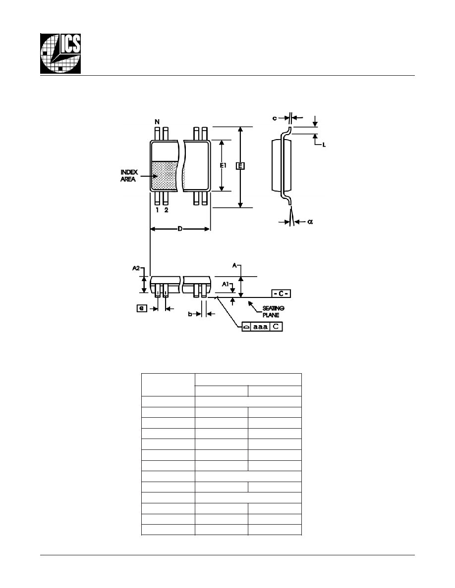
P
ACKAGE
O
UTLINE
- G S
UFFIX
FOR
20 L
EAD
TSSOP
T
ABLE
9. P
ACKAGE
D
IMENSIONS
Reference Document: JEDEC Publication 95, MO-153
L
O
B
M
Y
S
s
r
e
t
e
m
i
l
l
i
M
N
I
M
X
A
M
N
0
2
A
-
-
0
2
.
1
1
A
5
0
.
0
5
1
.
0
2
A
0
8
.
0
5
0
.
1
b
9
1
.
0
0
3
.
0
c
9
0
.
0
0
2
.
0
D
0
4
.
6
0
6
.
6
E
C
I
S
A
B
0
4
.
6
1
E
0
3
.
4
0
5
.
4
e
C
I
S
A
B
5
6
.
0
L
5
4
.
0
5
7
.
0
�
0
�
8
a
a
a
-
-
0
1
.
0
843002AG
www.icst.com/products/hiperclocks.html
REV. B MAY 6, 2005
15
Integrated
Circuit
Systems, Inc.
ICS843002
F
EMTO
C
LOCKS
TM C
RYSTAL
-
TO
-
3.3V LVPECL F
REQUENCY
S
YNTHESIZER
T
ABLE
10. O
RDERING
I
NFORMATION
While the information presented herein has been checked for both accuracy and reliability, Integrated Circuit Systems, Incorporated (ICS) assumes no responsibility for either its use
or for infringement of any patents or other rights of third parties, which would result from its use. No other circuits, patents, or licenses are implied. This product is intended for use
in normal commercial and industrial applications. Any other applications such as those requiring extended temperature range, high reliability, or other extraordinary environmental
requirements are not recommended without additional processing by ICS. ICS reserves the right to change any circuitry or specifications without notice. ICS does not authorize or
warrant any ICS product for use in life support devices or critical medical instruments.
r
e
b
m
u
N
r
e
d
r
O
/
t
r
a
P
g
n
i
k
r
a
M
e
g
a
k
c
a
P
g
n
i
g
a
k
c
a
P
g
n
i
p
p
i
h
S
e
r
u
t
a
r
e
p
m
e
T
G
A
2
0
0
3
4
8
S
C
I
G
A
2
0
0
3
4
8
S
C
I
P
O
S
S
T
d
a
e
L
0
2
e
b
u
t
C
�
5
8
o
t
C
�
0
3
-
T
G
A
2
0
0
3
4
8
S
C
I
G
A
2
0
0
3
4
8
S
C
I
P
O
S
S
T
d
a
e
L
0
2
l
e
e
r
&
e
p
a
t
0
0
5
2
C
�
5
8
o
t
C
�
0
3
-
F
L
G
A
2
0
0
3
4
8
S
C
I
F
L
A
2
0
0
3
4
8
S
C
I
P
O
S
S
T
"
e
e
r
F
-
d
a
e
L
"
d
a
e
L
0
2
e
b
u
t
C
�
5
8
o
t
C
�
0
3
-
T
F
L
G
A
2
0
0
3
4
8
S
C
I
F
L
A
2
0
0
3
4
8
S
C
I
P
O
S
S
T
"
e
e
r
F
-
d
a
e
L
"
d
a
e
L
0
2
l
e
e
r
&
e
p
a
t
0
0
5
2
C
�
5
8
o
t
C
�
0
3
-
.
t
n
a
il
p
m
o
c
S
H
o
R
e
r
a
d
n
a
n
o
i
t
a
r
u
g
i
f
n
o
c
e
e
r
F
-
b
P
e
h
t
e
r
a
r
e
b
m
u
n
t
r
a
p
e
h
t
o
t
"
F
L
"
n
a
h
t
i
w
d
e
r
e
d
r
o
e
r
a
t
a
h
t
s
t
r
a
P
:
E
T
O
N
The aforementioned trademark, HiPerClockSTM and F
EMTO
C
LOCKS
TM is a trademark of Integrated Circuit Systems, Inc. or its subsidiaries in the United States and/or other countries.

843002AG
www.icst.com/products/hiperclocks.html
REV. B MAY 6, 2005
16
Integrated
Circuit
Systems, Inc.
ICS843002
F
EMTO
C
LOCKS
TM C
RYSTAL
-
TO
-
3.3V LVPECL F
REQUENCY
S
YNTHESIZER
T
E
E
H
S
Y
R
O
T
S
I
H
N
O
I
S
I
V
E
R
v
e
R
e
l
b
a
T
e
g
a
P
e
g
n
a
h
C
f
o
n
o
i
t
p
i
r
c
s
e
D
e
t
a
D
A
1
.
e
l
b
a
T
n
o
i
t
c
n
u
F
n
o
i
t
c
e
l
e
S
y
c
n
e
u
q
e
r
F
e
h
t
o
t
z
H
M
5
.
7
8
1
d
e
d
d
A
4
0
/
6
2
/
8
A
0
1
T
5
1
.
r
e
b
m
u
n
t
r
a
p
e
e
r
F
d
a
e
L
d
e
d
d
a
-
e
l
b
a
T
n
o
i
t
a
m
r
o
f
n
I
g
n
i
r
e
d
r
O
4
0
/
0
3
/
9
A
5
T
4
f
,
o
p
y
t
d
e
t
c
e
r
r
o
c
-
e
l
b
a
T
s
c
i
t
s
i
r
e
t
c
a
r
a
h
C
C
A
T
U
O
.
n
i
m
7
6
.
6
8
1
o
t
.
n
i
m
7
6
.
0
8
1
4
0
/
7
2
/
2
1
A
0
1
T
1
5
1
t
u
p
t
u
o
.
.
.
s
t
r
o
p
p
u
S
"
d
a
e
r
o
t
t
e
ll
u
b
y
c
n
e
u
q
e
r
f
d
e
t
c
e
r
r
o
c
-
n
o
i
t
c
e
s
s
e
r
u
t
a
e
F
.
"
.
.
.
s
e
i
c
n
e
u
q
e
r
f
t
u
p
n
i
.
.
.
"
m
o
r
f
"
.
.
.
s
e
i
c
n
e
u
q
e
r
f
.
e
l
b
a
t
d
e
t
a
d
p
u
-
e
l
b
a
T
n
o
i
t
a
m
r
o
f
n
I
g
n
i
r
e
d
r
O
5
0
/
7
/
2
B
5
T
4
.
y
a
l
e
D
n
o
i
t
a
g
a
p
o
r
P
d
e
t
e
l
e
d
-
e
l
b
a
T
s
c
i
t
s
i
r
e
t
c
a
r
a
h
C
C
A
5
0
/
6
/
5