Document Outline
- General Description
- Features
- Pin Assignment
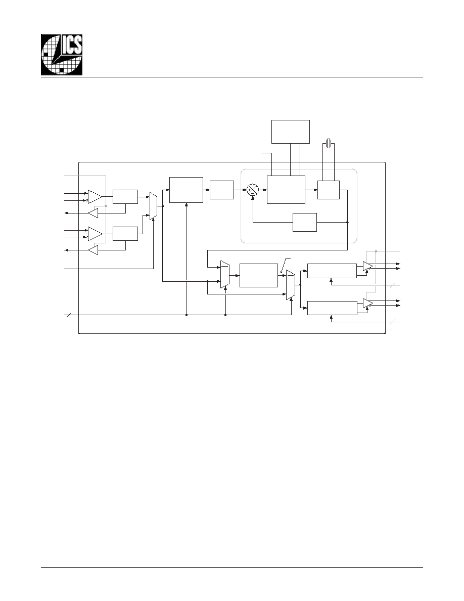
- Block Diagram
- Pin Descriptions
- Pin Characteristics
- Input Reference Selection Function Table
- Input Reference Divider Selection Function Table
- Output Divider Selection Function Table
- Absolute Maximum Ratings
- Power Supply DC Characteristics
- LVCMOS DC Characteristics
- Differential DC Characteristics
- LVPECL DC Characteristics
- Crystal Characteristics
- 3.3V AC Characteristics
- 3.3V/2.5V AC Characteristics
- Typical Phase Noise Plot
- Parameter Measurement Information
- Application Information
- Description of the PLL Stages
- VCXO PLL Loop Response Considerations
- Setting the VCXO PLL Loop Response
- External VCXO PLL Components
- Loss of Reference Indicator Output Pins
- Notes on Setting Charge Pump Current
- Power Supply Filtering Techniques
- Termination for 2.5V LVPECL Output
- Termination for 3.3V LVPECL Output
- Differential Clock Input Interface
- Single Ended Clock Input Interface
- Power Considerations
- Power Dissipation
- Junction Temperature
- Thermal Resistance
- Calculations & Equations
- LVPECL Driver Circuit & Termination Diagram
- Reliability Information
- Transistor Count
- Package Outline
- Package Dimensions
- Ordering Information
843002AKI-40
www.icst.com/products/hiperclocks.html
REV. A JUNE 22, 2005
1
Integrated
Circuit
Systems, Inc.
ICS843002I-40
175MH
Z
, F
EMTO
C
LOCKS
TM VCXO B
ASED
SONET/SDH J
ITTER
A
TTENUATOR
PRELIMINARY
G
ENERAL
D
ESCRIPTION
T h e I C S 8 4 3 0 0 2 I - 4 0 i s a m e m b e r o f t h e
HiperClockSTM family of high performance clock
solutions from ICS. The ICS843002I-40 is a PLL
based synchronous clock generator that is
optimized for SONET/SDH line card applications
where jitter attenuation and frequency translation is needed.
The device contains two internal PLL stages that are cascaded
in series. The first PLL stage uses a VCXO which is optimized
to provide reference clock jitter attenuation and to be jitter
tolerant, and to provide a stable reference clock for the 2nd
PLL stage (typically 19.44MHz). The second PLL stage
provides additional frequency multiplication (x32), and it
maintains low output jitter by using a low phase noise
FemtoClock VCO. PLL multiplication ratios are selected
from internal lookup tables using device input selection pins.
The device performance and the PLL multiplication ratios are
optimized to support non-FEC (non-Forward Error Correction)
SONET/SDH applications with rates up to OC-48 (SONET)
or STM-16 (SDH). The VCXO requires the use of an external,
inexpensive pullable crystal. VCXO PLL uses external passive
loop filter components which are used to optimize the PLL
loop bandwidth and damping characteristics for the given
line card application.
The ICS843002I-40 includes two clock input ports. Each one
can accept either a single-ended or differential input. Each
input port also includes an activity detector circuit, which
reports input clock activity through the LOR0 and LOR1 logic
output pins. The two input ports feed an input selection mux.
"Hitless switching" is accomplished through proper filter
tuning. Jitter transfer and wander characteristics are
influenced by loop filter tuning, and phase transient
performance is influenced by both loop filter tuning and
alignment error between the two reference clocks.
Typical ICS843002I-40 configuration in SONET/SDH Systems:
∑
VCXO 19.44MHz crystal
∑
Loop bandwidth: 50Hz - 250Hz
∑
Input Reference clock frequency selections:
19.44MHz, 38.88MHz, 77.76MHz, 155.52MHz,
311.04MHz, 622.08MHz
∑
Output clock frequency selections:
19.44MHz, 77.76MHz, 155.52MHz, Hi-Z
P
IN
A
SSIGNMENT
F
EATURES
∑ (2) Differential LVPECL outputs
∑ Selectable CLKx, nCLKx differential input pairs
∑ CLKx, nCLKx pairs can accept the following differential
input levels: LVPECL, LVDS, LVHSTL, SSTL, HCSL or
single-ended LVCMOS or LVTTL levels
∑ Maximum output frequency: 175MHz
∑ FemtoClock VCO frequency range: 560MHz - 700MHz
∑ RMS phase jitter @ 155.52MHz, using a 19.44MHz crystal
(12kHz to 20MHz): 0.81ps (typical)
∑ Full 3.3V or mixed 3.3V core/2.5V output supply voltage
∑ -40∞C to 85∞C ambient operating temperature
HiPerClockSTM
ICS
24
23
22
21
20
19
18
17
LOR0
LOR1
nc
V
CCO
_
LVCMOS
V
CCO
_
LVPECL
nQB
QB
V
EE
LF1
LF0
ISET
V
CC
CLK0
nCLK0
CLK_SEL
nc
QA_SEL1
QA_SEL0
nc
QB_SEL1
QB_SEL0
V
CCA
QA
nQA
nCLK1
CLK1
V
EE
R_SEL0
R_SEL1
R_SEL2
X
T
AL_OUT
X
T
AL_IN
ICS843002I-40
32-Lead VFQFN
5mm x 5mm x 0.75mm package body
K Package
Top View
The Preliminary Information presented herein represents a product in prototyping or pre-production. The noted characteristics are based on initial
product characterization. Integrated Circuit Systems, Incorporated (ICS) reserves the right to change any circuitry or specifications without notice.
32 31 30 29 28 27 26 25
9 10 11 12 13 14 15 16
1
2
3
4
5
6
7
8
843002AKI-40
www.icst.com/products/hiperclocks.html
REV. A JUNE 22, 2005
2
Integrated
Circuit
Systems, Inc.
ICS843002I-40
175MH
Z
, F
EMTO
C
LOCKS
TM VCXO B
ASED
SONET/SDH J
ITTER
A
TTENUATOR
PRELIMINARY
B
LOCK
D
IAGRAM
NOTE 1: 19.44MHz VCXO crystal shown is typical for SONET/SDH device applications.
R Divider =
1, 2, 4, 8,
16 or 32
CLK1
nCLK1
Activity
Detector
CLK0
nCLK0
Activity
Detector
LOR1
LOR0
R_SEL2:0
3
ISET
CLK_SEL
FemtoClock
PLL
x32
622.08 MHz
V
CCO_LVPECL
QA
nQA
C0 Divider =
4, 8, 32, or HiZ
QB
nQB
C1 Divider =
QB_SEL1:0
QA_SEL1:0
2
2
VCXO
Charge
Pump
and Loop
Filter
External
Loop
Components
19.44 MHz
Pullable
xtal
19.44 MHz
XT
AL_IN
XT
AL_OUT
LF1
LF0
Divide
by 32
Divide
by 32
VCXO Jitter Attenuation PLL
Phase
Detector
ICS843002-40
110
110
111
111
V
CCO_LVCMOS
1
0
4, 8, 32, or HiZ
843002AKI-40
www.icst.com/products/hiperclocks.html
REV. A JUNE 22, 2005
3
Integrated
Circuit
Systems, Inc.
ICS843002I-40
175MH
Z
, F
EMTO
C
LOCKS
TM VCXO B
ASED
SONET/SDH J
ITTER
A
TTENUATOR
PRELIMINARY
T
ABLE
1. P
IN
D
ESCRIPTIONS
r
e
b
m
u
N
e
m
a
N
e
p
y
T
n
o
i
t
p
i
r
c
s
e
D
2
,
1
0
F
L
,
1
F
L
g
o
l
a
n
A
t
u
p
t
u
O
/
t
u
p
n
I
.
s
n
i
p
e
d
o
n
n
o
i
t
c
e
n
n
o
c
r
e
t
li
f
p
o
o
L
3
T
E
S
I
g
o
l
a
n
A
t
u
p
t
u
O
/
t
u
p
n
I
.
n
i
p
g
n
i
t
t
e
s
t
n
e
r
r
u
c
p
m
u
p
e
g
r
a
h
C
4
V
C
C
r
e
w
o
P
.
n
i
p
y
l
p
p
u
s
r
e
w
o
p
e
r
o
C
5
0
K
L
C
t
u
p
n
I
n
w
o
d
ll
u
P
.
t
u
p
n
i
k
c
o
l
c
l
a
i
t
n
e
r
e
f
f
i
d
g
n
i
t
r
e
v
n
i
-
n
o
N
6
0
K
L
C
n
t
u
p
n
I
/
p
u
ll
u
P
n
w
o
d
ll
u
P
.
t
u
p
n
i
k
c
o
l
c
l
a
i
t
n
e
r
e
f
f
i
d
g
n
i
t
r
e
v
n
I
V
C
C
.
g
n
i
t
a
o
l
f
t
f
e
l
n
e
h
w
e
g
a
t
l
o
v
s
a
i
b
2
/
7
L
E
S
_
K
L
C
t
u
p
n
I
n
w
o
d
ll
u
P
.
A
3
e
l
b
a
T
e
e
S
.
s
l
e
v
e
l
e
c
a
f
r
e
t
n
i
L
T
T
V
L
/
S
O
M
C
V
L
.
t
c
e
l
e
s
k
c
o
l
c
t
u
p
n
I
,
9
0
1
,
1
L
E
S
_
A
Q
0
L
E
S
_
A
Q
t
u
p
n
I
p
u
ll
u
P
.
C
3
e
l
b
a
T
e
e
S
.
s
t
u
p
t
u
o
A
Q
n
/
A
Q
r
o
f
l
o
r
t
n
o
c
r
e
d
i
v
i
d
t
u
p
t
u
o
L
C
E
P
V
L
,
2
1
3
1
,
1
L
E
S
_
B
Q
0
L
E
S
_
B
Q
t
u
p
n
I
p
u
ll
u
P
.
C
3
e
l
b
a
T
e
e
S
.
s
t
u
p
t
u
o
B
Q
n
/
B
Q
r
o
f
l
o
r
t
n
o
c
r
e
d
i
v
i
d
t
u
p
t
u
o
L
C
E
P
V
L
4
1
V
A
C
C
r
e
w
o
P
.
n
i
p
y
l
p
p
u
s
g
o
l
a
n
A
6
1
,
5
1
A
Q
n
,
A
Q
t
u
p
t
u
O
.
s
l
e
v
e
l
e
c
a
f
r
e
t
n
i
L
C
E
P
V
L
.
r
i
a
p
t
u
p
t
u
o
k
c
o
l
c
l
a
i
t
n
e
r
e
f
f
i
D
7
2
,
7
1
V
E
E
r
e
w
o
P
.
s
n
i
p
y
l
p
p
u
s
e
v
i
t
a
g
e
N
9
1
,
8
1
B
Q
n
,
B
Q
t
u
p
t
u
O
.
s
l
e
v
e
l
e
c
a
f
r
e
t
n
i
L
C
E
P
V
L
.
r
i
a
p
t
u
p
t
u
o
k
c
o
l
c
l
a
i
t
n
e
r
e
f
f
i
D
0
2
V
L
C
E
P
V
L
_
O
C
C
r
e
w
o
P
.
B
Q
n
,
B
Q
d
n
a
A
Q
n
,
A
Q
r
o
f
n
i
p
y
l
p
p
u
s
r
e
w
o
p
t
u
p
t
u
O
1
2
V
S
O
M
C
V
L
_
O
C
C
r
e
w
o
P
.
1
R
O
L
d
n
a
0
R
O
L
r
o
f
n
i
p
y
l
p
p
u
s
r
e
w
o
P
2
2
,
1
1
,
8
c
n
d
e
s
u
n
U
.
t
c
e
n
n
o
c
o
N
3
2
1
R
O
L
t
u
p
t
u
O
.
1
K
L
C
r
o
f
e
c
n
e
r
e
f
e
r
f
o
s
s
o
l
,
t
u
p
t
u
o
m
r
a
l
A
.
s
l
e
v
e
l
e
c
a
f
r
e
t
n
i
L
T
T
V
L
/
S
O
M
C
V
L
4
2
0
R
O
L
t
u
p
t
u
O
.
0
K
L
C
r
o
f
e
c
n
e
r
e
f
e
r
f
o
s
s
o
l
,
t
u
p
t
u
o
m
r
a
l
A
.
s
l
e
v
e
l
e
c
a
f
r
e
t
n
i
L
T
T
V
L
/
S
O
M
C
V
L
5
2
1
K
L
C
n
t
u
p
n
I
/
p
u
ll
u
P
n
w
o
d
ll
u
P
.
t
u
p
n
i
k
c
o
l
c
l
a
i
t
n
e
r
e
f
f
i
d
g
n
i
t
r
e
v
n
I
V
C
C
.
g
n
i
t
a
o
l
f
t
f
e
l
n
e
h
w
e
g
a
t
l
o
v
s
a
i
b
2
/
6
2
1
K
L
C
t
u
p
n
I
n
w
o
d
ll
u
P
.
t
u
p
n
i
k
c
o
l
c
l
a
i
t
n
e
r
e
f
f
i
d
g
n
i
t
r
e
v
n
i
-
n
o
N
,
8
2
,
9
2
0
3
,
0
L
E
S
_
R
,
1
L
E
S
_
R
2
L
E
S
_
R
t
u
p
n
I
n
w
o
d
ll
u
P
.
B
3
e
l
b
a
T
e
e
S
.
e
c
a
f
r
e
t
n
i
L
T
T
V
L
/
S
O
M
C
V
L
.
n
o
i
t
c
e
l
e
s
r
e
d
i
v
i
d
t
u
p
n
I
,
1
3
2
3
,
T
U
O
_
L
A
T
X
N
I
_
L
A
T
X
t
u
p
n
I
.
t
u
p
t
u
o
e
h
t
s
i
T
U
O
_
L
A
T
X
.
e
c
a
f
r
e
t
n
i
r
o
t
a
ll
i
c
s
o
l
a
t
s
y
r
C
.
t
u
p
n
i
e
h
t
s
i
N
I
_
L
A
T
X
:
E
T
O
N
p
u
ll
u
P
d
n
a
n
w
o
d
ll
u
P
.
s
e
u
l
a
v
l
a
c
i
p
y
t
r
o
f
,
s
c
i
t
s
i
r
e
t
c
a
r
a
h
C
n
i
P
,
2
e
l
b
a
T
e
e
S
.
s
r
o
t
s
i
s
e
r
t
u
p
n
i
l
a
n
r
e
t
n
i
o
t
r
e
f
e
r
T
ABLE
2. P
IN
C
HARACTERISTICS
l
o
b
m
y
S
r
e
t
e
m
a
r
a
P
s
n
o
i
t
i
d
n
o
C
t
s
e
T
m
u
m
i
n
i
M
l
a
c
i
p
y
T
m
u
m
i
x
a
M
s
t
i
n
U
C
N
I
e
c
n
a
t
i
c
a
p
a
C
t
u
p
n
I
4
F
p
R
P
U
L
L
U
P
r
o
t
s
i
s
e
R
p
u
ll
u
P
t
u
p
n
I
0
5
k
R
N
W
O
D
L
L
U
P
r
o
t
s
i
s
e
R
n
w
o
d
ll
u
P
t
u
p
n
I
0
5
k

843002AKI-40
www.icst.com/products/hiperclocks.html
REV. A JUNE 22, 2005
4
Integrated
Circuit
Systems, Inc.
ICS843002I-40
175MH
Z
, F
EMTO
C
LOCKS
TM VCXO B
ASED
SONET/SDH J
ITTER
A
TTENUATOR
PRELIMINARY
T
ABLE
3A. I
NPUT
R
EFERENCE
S
ELECTION
F
UNCTION
T
ABLE
s
t
u
p
n
I
L
E
S
_
K
L
C
d
e
t
c
e
l
e
S
t
u
p
n
I
0
0
K
L
C
1
1
K
L
C
T
ABLE
3B. I
NPUT
R
EFERENCE
D
IVIDER
S
ELECTION
F
UNCTION
T
ABLE
s
t
u
p
n
I
0
:
2
L
E
S
_
R
e
t
a
t
S
r
o
e
u
l
a
V
r
e
d
i
v
i
D
R
0
0
0
1
˜
1
0
0
2
˜
0
1
0
4
˜
1
1
0
8
˜
0
0
1
6
1
˜
1
0
1
2
3
˜
0
1
1
L
L
P
O
X
C
V
s
s
a
p
y
b
1
1
1
s
'
L
L
P
TM
k
c
o
l
C
o
t
m
e
F
d
n
a
O
X
C
V
s
s
a
p
y
b
T
ABLE
3C. O
UTPUT
D
IVIDER
S
ELECTION
F
UNCTION
T
ABLE
s
t
u
p
n
I
0
:
1
L
E
S
_
x
Q
e
t
a
t
S
r
o
e
u
l
a
V
r
e
d
i
v
i
D
t
u
p
t
u
O
0
0
Z
-
i
H
Q
n
d
n
a
Q
t
u
p
t
u
O
1
0
2
3
˜
0
1
8
˜
1
1
4
˜

843002AKI-40
www.icst.com/products/hiperclocks.html
REV. A JUNE 22, 2005
5
Integrated
Circuit
Systems, Inc.
ICS843002I-40
175MH
Z
, F
EMTO
C
LOCKS
TM VCXO B
ASED
SONET/SDH J
ITTER
A
TTENUATOR
PRELIMINARY
T
ABLE
4A. P
OWER
S
UPPLY
DC C
HARACTERISTICS
,
V
CC
= V
CCA
= 3.3V±5%, V
CCO_LVCMOS
, V
CCO_LVPECL
= 3.3V±5%
OR
2.5V±5%,
T
A
= -40∞C
TO
85∞C
A
BSOLUTE
M
AXIMUM
R
ATINGS
Supply Voltage, V
CC
4.6V
Inputs, V
I
-0.5V to V
CC
+ 0.5V
Outputs, V
O
(LVCMOS)
-0.5V to V
CCO
+ 0.5V
Outputs, I
O
(LVPECL)
Continuous Current
50mA
Surge Current
100mA
Package Thermal Impedance,
JA
34.8∞C/W (0 lfpm)
Storage Temperature, T
STG
-65∞C to 150∞C
NOTE: Stresses beyond those listed under Absolute
Maximum Ratings may cause permanent damage to the
device. These ratings are stress specifications only. Functional
operation of product at these conditions or any conditions be-
yond those listed in the
DC Characteristics or AC Character-
istics is not implied. Exposure to absolute maximum rating
conditions for extended periods may affect product reliability.
l
o
b
m
y
S
r
e
t
e
m
a
r
a
P
s
n
o
i
t
i
d
n
o
C
t
s
e
T
m
u
m
i
n
i
M
l
a
c
i
p
y
T
m
u
m
i
x
a
M
s
t
i
n
U
V
C
C
e
g
a
t
l
o
V
y
l
p
p
u
S
e
r
o
C
5
3
1
.
3
3
.
3
5
6
4
.
3
V
V
A
C
C
e
g
a
t
l
o
V
y
l
p
p
u
S
g
o
l
a
n
A
5
3
1
.
3
3
.
3
5
6
4
.
3
V
V
,
S
O
M
C
V
L
_
O
C
C
V
L
C
E
P
V
L
_
O
C
C
e
g
a
t
l
o
V
y
l
p
p
u
S
t
u
p
t
u
O
5
3
1
.
3
3
.
3
5
6
4
.
3
V
5
7
3
.
2
5
.
2
5
2
6
.
2
V
I
E
E
t
n
e
r
r
u
C
y
l
p
p
u
S
r
e
w
o
P
5
7
1
A
m
I
A
C
C
t
n
e
r
r
u
C
y
l
p
p
u
S
g
o
l
a
n
A
0
1
A
m
T
ABLE
4B. LVCMOS / LVTTL DC C
HARACTERISTICS
,
V
CC
= V
CCA
= 3.3V±5%, V
CCO_LVCMOS
= 3.3V±5%
OR
2.5V±5%,
T
A
= -40∞C
TO
85∞C
l
o
b
m
y
S
r
e
t
e
m
a
r
a
P
s
n
o
i
t
i
d
n
o
C
t
s
e
T
m
u
m
i
n
i
M
l
a
c
i
p
y
T
m
u
m
i
x
a
M
s
t
i
n
U
V
H
I
t
u
p
n
I
e
g
a
t
l
o
V
h
g
i
H
2
V
C
C
3
.
0
+
V
V
L
I
e
g
a
t
l
o
V
w
o
L
t
u
p
n
I
3
.
0
-
8
.
0
V
I
H
I
t
u
p
n
I
t
n
e
r
r
u
C
h
g
i
H
2
:
0
L
E
S
_
R
,
L
E
S
_
K
L
C
V
C
C
V
=
N
I
V
5
6
4
.
3
=
0
5
1
A
µ
1
:
0
L
E
S
_
B
Q
,
1
:
0
L
E
S
_
A
Q
V
C
C
V
=
N
I
V
5
6
4
.
3
=
5
A
µ
I
L
I
t
u
p
n
I
t
n
e
r
r
u
C
w
o
L
2
:
0
L
E
S
_
R
,
L
E
S
_
K
L
C
V
C
C
,
V
5
6
4
.
3
=
V
N
I
V
0
=
5
-
A
µ
1
:
0
L
E
S
_
B
Q
,
1
:
0
L
E
S
_
A
Q
V
C
C
,
V
5
6
4
.
3
=
V
N
I
V
0
=
0
5
1
-
A
µ
V
H
O
t
u
p
t
u
O
e
g
a
t
l
o
V
h
g
i
H
1
E
T
O
N
;
1
R
O
L
,
0
R
O
L
V
S
O
M
C
V
L
_
O
C
C
V
3
.
3
=
6
.
2
V
V
S
O
M
C
V
L
_
O
C
C
V
5
.
2
=
8
.
1
V
V
L
O
t
u
p
t
u
O
e
g
a
t
l
o
V
w
o
L
1
E
T
O
N
;
1
R
O
L
,
0
R
O
L
V
S
O
M
C
V
L
_
O
C
C
V
5
.
2
r
o
V
3
.
3
=
5
.
0
V
NOTE 1: Outputs terminated with 50
to V
CCO_LVCMOS
/2 .See Parameter Measurement Information Section,
"Output Load Test Circuit".

843002AKI-40
www.icst.com/products/hiperclocks.html
REV. A JUNE 22, 2005
6
Integrated
Circuit
Systems, Inc.
ICS843002I-40
175MH
Z
, F
EMTO
C
LOCKS
TM VCXO B
ASED
SONET/SDH J
ITTER
A
TTENUATOR
PRELIMINARY
T
ABLE
4D. LVPECL DC C
HARACTERISTICS
,
V
CC
= V
CCA
= 3.3V±5%, V
CCO_LVPECL
= 3.3V±5%
OR
2.5V±5%, T
A
= -40∞C
TO
85∞C
l
o
b
m
y
S
r
e
t
e
m
a
r
a
P
s
n
o
i
t
i
d
n
o
C
t
s
e
T
m
u
m
i
n
i
M
l
a
c
i
p
y
T
m
u
m
i
x
a
M
s
t
i
n
U
V
H
O
1
E
T
O
N
;
e
g
a
t
l
o
V
h
g
i
H
t
u
p
t
u
O
V
O
C
C
4
.
1
-
V
O
C
C
9
.
0
-
V
V
L
O
1
E
T
O
N
;
e
g
a
t
l
o
V
w
o
L
t
u
p
t
u
O
V
O
C
C
0
.
2
-
V
O
C
C
7
.
1
-
V
V
G
N
I
W
S
g
n
i
w
S
e
g
a
t
l
o
V
t
u
p
t
u
O
k
a
e
P
-
o
t
-
k
a
e
P
6
.
0
0
.
1
V
0
5
h
t
i
w
d
e
t
a
n
i
m
r
e
t
s
t
u
p
t
u
O
:
1
E
T
O
N
V
o
t
L
C
E
P
V
L
_
O
C
C
,
n
o
i
t
c
e
s
"
n
o
i
t
a
m
r
o
f
n
I
t
n
e
m
e
r
u
s
a
e
M
r
e
t
e
m
a
r
a
P
"
e
e
S
.
V
2
-
.
"
t
i
u
c
r
i
C
t
s
e
T
d
a
o
L
t
u
p
t
u
O
"
T
ABLE
5. C
RYSTAL
C
HARACTERISTICS
l
o
b
m
y
S
r
e
t
e
m
a
r
a
P
s
n
o
i
t
i
d
n
o
C
t
s
e
T
m
u
m
i
n
i
M
l
a
c
i
p
y
T
m
u
m
i
x
a
M
s
t
i
n
U
f
N
y
c
n
e
u
q
e
r
F
l
a
n
i
m
o
N
4
4
.
9
1
z
H
M
f
T
e
c
n
a
r
e
l
o
T
y
c
n
e
u
q
e
r
F
D
B
T
±
m
p
p
f
S
y
t
il
i
b
a
t
S
y
c
n
e
u
q
e
r
F
D
B
T
±
m
p
p
e
g
n
a
R
e
r
u
t
a
r
e
p
m
e
T
g
n
i
t
a
r
e
p
O
0
0
7
C
∞
C
L
e
c
n
a
t
i
c
a
p
a
C
d
a
o
L
2
1
F
p
C
O
e
c
n
a
t
i
c
a
p
a
C
t
n
u
h
S
4
F
p
C
O
C
/
1
o
i
t
a
R
y
t
il
i
b
a
ll
u
P
0
2
2
0
4
2
R
S
E
e
c
n
a
t
s
i
s
e
R
s
e
i
r
e
S
t
n
e
l
a
v
i
u
q
E
0
5
l
e
v
e
L
e
v
i
r
D
1
W
m
n
o
i
t
a
r
e
p
O
f
o
e
d
o
M
l
a
t
n
e
m
a
d
n
u
F
T
ABLE
4C. D
IFFERENTIAL
DC C
HARACTERISTICS
,
V
CC
= V
CCA
= 3.3V±5%, V
CCO_LVPECL
= 3.3V±5%
OR
2.5V±5%,
T
A
= -40∞C
TO
85∞C
l
o
b
m
y
S
r
e
t
e
m
a
r
a
P
s
n
o
i
t
i
d
n
o
C
t
s
e
T
m
u
m
i
n
i
M
l
a
c
i
p
y
T
m
u
m
i
x
a
M
s
t
i
n
U
I
H
I
t
n
e
r
r
u
C
h
g
i
H
t
u
p
n
I
1
K
L
C
,
0
K
L
C
V
N
I
V
=
C
C
V
5
6
4
.
3
=
0
5
1
A
µ
1
K
L
C
n
,
0
K
L
C
n
0
5
1
A
µ
I
L
I
t
n
e
r
r
u
C
w
o
L
t
u
p
n
I
1
K
L
C
,
0
K
L
C
V
N
I
V
,
V
0
=
C
C
V
5
6
4
.
3
=
5
-
A
µ
1
K
L
C
n
,
0
K
L
C
n
V
N
I
V
,
V
0
=
C
C
V
5
6
4
.
3
=
0
5
1
-
A
µ
V
P
P
e
g
a
t
l
o
V
t
u
p
n
I
k
a
e
P
-
o
t
-
k
a
e
P
5
1
.
0
3
.
1
V
V
R
M
C
2
,
1
E
T
O
N
;
e
g
a
t
l
o
V
t
u
p
n
I
e
d
o
M
n
o
m
m
o
C
V
E
E
5
.
0
+
V
C
C
5
8
.
0
-
V
V
s
a
d
e
n
i
f
e
d
s
i
e
g
a
t
l
o
v
e
d
o
m
n
o
m
m
o
C
:
1
E
T
O
N
H
I
.
V
s
i
x
K
L
C
n
,
x
K
L
C
r
o
f
e
g
a
t
l
o
v
t
u
p
n
i
m
u
m
i
x
a
m
e
h
t
,
s
n
o
i
t
a
c
il
p
p
a
d
e
d
n
e
e
l
g
n
i
s
r
o
F
:
2
E
T
O
N
C
C
.
V
3
.
0
+

843002AKI-40
www.icst.com/products/hiperclocks.html
REV. A JUNE 22, 2005
7
Integrated
Circuit
Systems, Inc.
ICS843002I-40
175MH
Z
, F
EMTO
C
LOCKS
TM VCXO B
ASED
SONET/SDH J
ITTER
A
TTENUATOR
PRELIMINARY
T
ABLE
6A. AC C
HARACTERISTICS
,
V
CC
= V
CCA
= V
CCO_LVCMOS
, V
CCO_LVPECL
= 3.3V±5%, T
A
= -40∞C
TO
85∞C
l
o
b
m
y
S
r
e
t
e
m
a
r
a
P
s
n
o
i
t
i
d
n
o
C
t
s
e
T
m
u
m
i
n
i
M
l
a
c
i
p
y
T
m
u
m
i
x
a
M
s
t
i
n
U
F
T
U
O
y
c
n
e
u
q
e
r
F
t
u
p
t
u
O
4
4
.
9
1
5
7
1
z
H
M
t
)
¯
(
t
ij
;
)
m
o
d
n
a
R
(
,
r
e
t
t
i
J
e
s
a
h
P
S
M
R
1
E
T
O
N
:
e
g
n
a
r
n
o
i
t
a
r
g
e
t
n
I
,
z
H
M
2
5
.
5
5
1
z
H
M
0
2
-
z
H
k
2
1
1
8
.
0
s
p
t
)
o
(
k
s
3
,
2
E
T
O
N
;
w
e
k
S
t
u
p
t
u
O
5
0
1
s
p
t
R
t
/
F
e
m
i
T
ll
a
F
/
e
s
i
R
t
u
p
t
u
O
%
0
8
o
t
%
0
2
0
9
8
s
p
c
d
o
e
l
c
y
C
y
t
u
D
t
u
p
t
u
O
0
5
%
.
n
o
i
t
c
e
s
n
o
i
t
a
m
r
o
f
n
I
t
n
e
m
e
r
u
s
a
e
M
r
e
t
e
m
a
r
a
P
e
e
S
.
t
o
l
P
e
s
i
o
N
e
s
a
h
P
e
h
t
o
t
r
e
f
e
r
e
s
a
e
l
P
:
1
E
T
O
N
.
s
n
o
i
t
i
d
n
o
c
d
a
o
l
l
a
u
q
e
h
t
i
w
d
n
a
e
g
a
t
l
o
v
y
l
p
p
u
s
e
m
a
s
e
h
t
t
a
s
t
u
p
t
u
o
n
e
e
w
t
e
b
w
e
k
s
s
a
d
e
n
i
f
e
D
:
2
E
T
O
N
.
s
t
n
i
o
p
s
s
o
r
c
l
a
i
t
n
e
r
e
f
f
i
d
t
u
p
t
u
o
e
h
t
t
a
d
e
r
u
s
a
e
M
.
5
6
d
r
a
d
n
a
t
S
C
E
D
E
J
h
t
i
w
e
c
n
a
d
r
o
c
c
a
n
i
d
e
n
i
f
e
d
s
i
r
e
t
e
m
a
r
a
p
s
i
h
T
:
3
E
T
O
N
T
ABLE
6B. AC C
HARACTERISTICS
,
V
CC
= V
CCA
= 3.3V±5%, V
CCO_LVCMOS
, V
CCO_LVPECL
= 2.5V±5%, T
A
= -40∞C
TO
85∞C
l
o
b
m
y
S
r
e
t
e
m
a
r
a
P
s
n
o
i
t
i
d
n
o
C
t
s
e
T
m
u
m
i
n
i
M
l
a
c
i
p
y
T
m
u
m
i
x
a
M
s
t
i
n
U
F
T
U
O
y
c
n
e
u
q
e
r
F
t
u
p
t
u
O
4
4
.
9
1
5
7
1
z
H
M
t
)
¯
(
t
ij
;
)
m
o
d
n
a
R
(
,
r
e
t
t
i
J
e
s
a
h
P
S
M
R
1
E
T
O
N
:
e
g
n
a
r
n
o
i
t
a
r
g
e
t
n
I
,
z
H
M
2
5
.
5
5
1
z
H
M
0
2
-
z
H
k
2
1
3
8
.
0
s
p
t
)
o
(
k
s
3
,
2
E
T
O
N
;
w
e
k
S
t
u
p
t
u
O
5
9
s
p
t
R
t
/
F
e
m
i
T
ll
a
F
/
e
s
i
R
t
u
p
t
u
O
%
0
8
o
t
%
0
2
0
0
9
s
p
c
d
o
e
l
c
y
C
y
t
u
D
t
u
p
t
u
O
0
5
%
.
n
o
i
t
c
e
s
n
o
i
t
a
m
r
o
f
n
I
t
n
e
m
e
r
u
s
a
e
M
r
e
t
e
m
a
r
a
P
e
e
S
.
t
o
l
P
e
s
i
o
N
e
s
a
h
P
e
h
t
o
t
r
e
f
e
r
e
s
a
e
l
P
:
1
E
T
O
N
.
s
n
o
i
t
i
d
n
o
c
d
a
o
l
l
a
u
q
e
h
t
i
w
d
n
a
e
g
a
t
l
o
v
y
l
p
p
u
s
e
m
a
s
e
h
t
t
a
s
t
u
p
t
u
o
n
e
e
w
t
e
b
w
e
k
s
s
a
d
e
n
i
f
e
D
:
2
E
T
O
N
.
s
t
n
i
o
p
s
s
o
r
c
l
a
i
t
n
e
r
e
f
f
i
d
t
u
p
t
u
o
e
h
t
t
a
d
e
r
u
s
a
e
M
.
5
6
d
r
a
d
n
a
t
S
C
E
D
E
J
h
t
i
w
e
c
n
a
d
r
o
c
c
a
n
i
d
e
n
i
f
e
d
s
i
r
e
t
e
m
a
r
a
p
s
i
h
T
:
3
E
T
O
N

843002AKI-40
www.icst.com/products/hiperclocks.html
REV. A JUNE 22, 2005
8
Integrated
Circuit
Systems, Inc.
ICS843002I-40
175MH
Z
, F
EMTO
C
LOCKS
TM VCXO B
ASED
SONET/SDH J
ITTER
A
TTENUATOR
PRELIMINARY
T
YPICAL
P
HASE
N
OISE
AT
155.52MH
Z
155.52MHz
RMS Phase Jitter (Random)
12kHz to 20MHz = 0.81ps (typical)
O
FFSET
F
REQUENCY
(H
Z
)
N
OISE
P
O
WER
dBc
Hz
0
-10
-20
-30
-40
-50
-60
-70
-80
-90
-100
-110
-120
-130
-140
-150
-160
-170
-180
-190
1k
10k
100k
1M
10M
100M
Filter
Raw Phase Noise Data
Phase Noise Result by adding
Filter to raw data

843002AKI-40
www.icst.com/products/hiperclocks.html
REV. A JUNE 22, 2005
9
Integrated
Circuit
Systems, Inc.
ICS843002I-40
175MH
Z
, F
EMTO
C
LOCKS
TM VCXO B
ASED
SONET/SDH J
ITTER
A
TTENUATOR
PRELIMINARY
P
ARAMETER
M
EASUREMENT
I
NFORMATION
O
UTPUT
S
KEW
3.3V C
ORE
/2.5V LVPECL O
UTPUT
L
OAD
AC T
EST
C
IRCUIT
3.3V C
ORE
/3.3V LVPECL O
UTPUT
L
OAD
AC T
EST
C
IRCUIT
SCOPE
Qx
nQx
LVPECL
2.8V±0.04V
O
UTPUT
R
ISE
/F
ALL
T
IME
-0.5V ± 0.125V
tsk(o)
nQx
Qx
nQy
Qy
Clock
Outputs
20%
80%
80%
20%
t
R
t
F
V
SW I N G
t
PW
t
PERIOD
t
PW
t
PERIOD
odc =
x 100%
QA, QB
nQA, nQB
V
EE
Phase Noise Mask
Offset Frequency
f
1
f
2
Phase Noise Plot
RMS Jitter = Area Under the Masked Phase Noise Plot
Noise P
o
w
er
2V
O
UTPUT
D
UTY
C
YCLE
/P
ULSE
W
IDTH
/tP
ERIOD
V
CMR
Cross Points
V
PP
V
EE
nCLK0,
nCLK1
nCLK0,
nCLK1
V
CC
D
IFFERENTIAL
I
NPUT
L
EVEL
P
HASE
J
ITTER
SCOPE
Qx
nQx
LVPECL
-1.3V ± 0.165V
V
EE
V
CC
,
V
CCA,
V
CCO_LVPECL
2V
V
CCO_LVPECL
V
CC
,
V
CCA
843002AKI-40
www.icst.com/products/hiperclocks.html
REV. A JUNE 22, 2005
10
Integrated
Circuit
Systems, Inc.
ICS843002I-40
175MH
Z
, F
EMTO
C
LOCKS
TM VCXO B
ASED
SONET/SDH J
ITTER
A
TTENUATOR
PRELIMINARY
A
PPLICATION
I
NFORMATION
D
ESCRIPTION
OF
THE
PLL S
TAGES
The ICS843002I-40 is a two stage device, a VCXO PLL
followed by a low phase noise FemtoClock PLL. The VCXO
uses an external pullable crystal which can be pulled
±100ppm by the VCXO PLL circuitry to phase lock it to
the input reference frequency. The FemtoClock PLL is a
wide bandwidth PLL (about 800kHz) which means it will
phase track the VCXO PLL. Most of the reference clock
jitter attenuation needs to be accomplished by VCXO PLL.
By using the bypass FemtoClock PLL mode (Table 3B),
the selected input reference clock can be passed directly
to the FemtoClock PLL which will multiply it up by 32 to a
higher frequency. A second mode, VCXO and FemtoClock
bypass, routes the selected input refrence directly to the
LVPECL output dividers.
VCXO PLL L
OOP
R
ESPONSE
C
ONSIDERATIONS
Loop response characteristics of the VCXO PLL is affected
by the VCXO feedback divider value (bandwidth and damp-
ing factor), and by the external loop filter components
(bandwidth, damping factor, and 2
nd
frequency response).
A practical range of VCXO PLL bandwidth is from about
10Hz to about 1kHz. The setting of VCXO PLL bandwidth
and damping factor is covered later in this document. A
PC based PLL bandwidth calculator is also under devel-
opment. For assistance with loop bandwidth suggestions
or value calculation, please contact ICS applications.
S
ETTING
THE
VCXO PLL L
OOP
R
ESPONSE
The VCXO PLL loop response is determined both by fixed
device characteristics and by other characteristics set by the
user. This includes the values of R
S
, C
S
, C
P
and R
SET
as shown
in the External VCXO PLL Components figure on this page.
The VCXO PLL loop bandwidth is approximated by:
W
HERE
:
R
S
= Value of resistor R
S
in loop filter in Ohms
I
CP
= Charge pump current in amps (see table on page 12)
K
O
= VCXO Gain in Hz/V
The above equation calculates the "normalized" loop bandwidth
(denoted as "NBW") which is approximately equal to the - 3dB
bandwidth. NBW does not take into account the effects of
damping factor or the second pole imposed by C
P
. It does,
however, provide a useful approximation of filter performance.
To prevent jitter on the clock output due to modulation of the
VCXO PLL by the phase detector frequency, the following general
rule should be observed:
(Phase Detector) = Input Frequency ˜ (R Divider x 32)
The PLL loop damping factor is determined by:
W
HERE
:
C
S
= Value of capacitor C
S
in loop filter in Farads
NBW (VCXO PLL) =
R
S
x I
CP
x K
O
32
NBW (VCXO PLL)
(Phase Detector)
20
DF (VCLK) = x
R
S
2
I
CP
x C
S
x K
O
32

843002AKI-40
www.icst.com/products/hiperclocks.html
REV. A JUNE 22, 2005
11
Integrated
Circuit
Systems, Inc.
ICS843002I-40
175MH
Z
, F
EMTO
C
LOCKS
TM VCXO B
ASED
SONET/SDH J
ITTER
A
TTENUATOR
PRELIMINARY
N
OTES
ON
S
ETTING
THE
V
ALUE
OF
C
P
As another general rule, the following relationship should be
maintained between components C
S
and C
P
in the loop filter:
C
P
establishes a second pole in the VCXO PLL loop filter. For
higher damping factors (> 1), calculate the value of C
P
based on
a C
S
value that would be used for a damping factor of 1. This will
minimize baseband peaking and loop instability that can lead to
output jitter.
C
P
also dampens VCXO PLL input voltage modulation by the
charge pump correction pulses. A C
P
value that is too low will
result in increased output phase noise at the phase detector
frequency due to this. In extreme cases where input jitter is high,
charge pump current is high, and C
P
is too small, the VCXO PLL
input voltage can hit the supply or ground rail resulting in non-
linear loop response.
The best way to set the value of C
P
is to use the filter response
software under development from ICS (please refer to the
following section). C
P
should be increased in value until it just
starts affecting the passband peak.
L
OOP
F
ILTER
R
ESPONSE
S
OFTWARE
Online tools to calculate loop filter response (coming soon) at
www.icst.com. Contact your local sales representative if a tool
cannot be found for this product.
N
OTES
ON
E
XTERNAL
C
RYSTAL
L
OAD
C
APACITORS
In the loop filter schematic diagram, capacitors are shown be-
tween pins 32 to ground and between pins 31 to ground. These
are optional crystal load capacitors which can be used to cen-
ter tune the external pullable crystal (the crystal frequency can
only be lowered by adding capacitance, it cannot be raised).
Note that the addition of external load capacitors will decrease
the crystal pull range and the Kvco value.
C
P
=
C
S
20
1
2
3
32 31
LF1
LF0
ISET
C
S
R
S
C
P
R
SET
The external crystal devices and loop filter components should
be kept close to the device. Loop filter and crystal PCB
connection traces should be kept short and well separated from
each other and from other signal traces. Other signal traces
should not run underneath the device, the loop filter or crystal
components.
E
XTERNAL
VCXO PLL C
OMPONENTS
In general, the loop damping factor should be 0.7 or greater to
ensure output stability. A higher damping factor will create less
peaking in the passband. A higher damping factor may also
increase lock time and output clock jitter when there is excess
digital noise in the system application, due to the reduced ability
of the PLL to respond to and therefore compensate for phase
noise ingress.
The LOR0 and LOR1 pins are controlled by the internal clock
activity monitor circuits. The clock activity monitor circuits are
clocked by the VCXO PLL phase detector feedback clock.
The LOR output is asserted high if there are three consecutive
feedback clock edges without any reference clock edges (in
both cases, either a negative or positive transition is counted
L
OSS
OF
R
EFERENCE
I
NDICATOR
(LOR0
AND
LOR1) O
UTPUT
P
INS
.
as an "edge"). The LOR output will otherwise be low. The
activity monitor does not flag excessive reference transitions in
an phase detector observation interval as an error. The monitor
only distinguishes between transitions occurring and no transi-
tions occurring.

843002AKI-40
www.icst.com/products/hiperclocks.html
REV. A JUNE 22, 2005
12
Integrated
Circuit
Systems, Inc.
ICS843002I-40
175MH
Z
, F
EMTO
C
LOCKS
TM VCXO B
ASED
SONET/SDH J
ITTER
A
TTENUATOR
PRELIMINARY
N
OTES
ON
S
ETTING
C
HARGE
P
UMP
C
URRENT
The recommended range for the charge pump current is 50
A
to 300
A. Below 50A, loop filter charge leakage, due to PCB or
capacitor leakage, can become a problem. This loop filter leakage
can cause locking problems, output clock cycle slips, or low
frequency phase noise.
1E-3
100E-6
10E-6
1k
10k
100k
R
SET
,
I
CP
, Amps
R
T
E
S
I
(
t
n
e
r
r
u
C
p
m
u
P
e
g
r
a
h
C
P
C
)
k
6
.
7
1
A
µ
5
.
2
6
k
8
.
8
A
µ
5
2
1
k
4
.
4
A
µ
0
5
2
k
2
.
2
A
µ
0
0
5
F
IGURE
1. C
HARGE
P
UMP
C
URRENT
VS
. V
ALUE
OF
R
SET
(
EXTERNAL
RESISTOR
) G
RAPH
As can be seen in the loop bandwidth and damping factor
equations or by using the filter response software available from
ICS, increasing charge pump current (I
CP
) increases both
bandwidth and damping factor.
C
HARGE
P
UMP
C
URRENT
, E
XAMPLE
S
ETTINGS

843002AKI-40
www.icst.com/products/hiperclocks.html
REV. A JUNE 22, 2005
13
Integrated
Circuit
Systems, Inc.
ICS843002I-40
175MH
Z
, F
EMTO
C
LOCKS
TM VCXO B
ASED
SONET/SDH J
ITTER
A
TTENUATOR
PRELIMINARY
T
ERMINATION
FOR
2.5V LVPECL O
UTPUT
Figure 3A and Figure 3B show examples of termination for 2.5V
LVPECL driver. These terminations are equivalent to terminat-
ing 50
to V
CC
- 2V. For V
CC
= 2.5V, the V
CC
- 2V is very close to
ground level. The R3 in Figure 3B can be eliminated and the
termination is shown in
Figure 3C.
F
IGURE
3C. 2.5V LVPECL T
ERMINATION
E
XAMPLE
F
IGURE
3B. 2.5V LVPECL D
RIVER
T
ERMINATION
E
XAMPLE
F
IGURE
3A. 2.5V LVPECL D
RIVER
T
ERMINATION
E
XAMPLE
R2
62.5
Zo = 50 Ohm
R1
250
+
-
2.5V
2,5V LVPECL
Driv er
R4
62.5
R3
250
Zo = 50 Ohm
2.5V
VCC=2.5V
R1
50
R3
18
Zo = 50 Ohm
Zo = 50 Ohm
+
-
2,5V LVPECL
Driv er
VCC=2.5V
2.5V
R2
50
2,5V LVPECL
Driv er
VCC=2.5V
R1
50
R2
50
2.5V
Zo = 50 Ohm
Zo = 50 Ohm
+
-
As in any high speed analog circuitry, the power supply pins
are vulnerable to random noise. The ICS843002I-40 provides
separate power supplies to isolate any high switching
noise from the outputs to the internal PLL. V
CC
, V
CCA
, and V
CCO_X
should be individually connected to the power supply
plane through vias, and bypass capacitors should be
used for each pin. To achieve optimum jitter performance,
power supply isolation is required.
Figure 2 illustrates how
a 10
resistor along with a 10F and a .01F bypass
capacitor should be connected to each V
CCA
pin.
P
OWER
S
UPPLY
F
ILTERING
T
ECHNIQUES
F
IGURE
2. P
OWER
S
UPPLY
F
ILTERING
10
V
CCA
10
F
.01
F
3.3V
.01
F
V
CC

843002AKI-40
www.icst.com/products/hiperclocks.html
REV. A JUNE 22, 2005
14
Integrated
Circuit
Systems, Inc.
ICS843002I-40
175MH
Z
, F
EMTO
C
LOCKS
TM VCXO B
ASED
SONET/SDH J
ITTER
A
TTENUATOR
PRELIMINARY
V
CC
- 2V
50
50
RTT
Z
o
= 50
Z
o
= 50
FOUT
FIN
RTT =
Z
o
1
((V
OH
+ V
OL
) / (V
CC
≠ 2)) ≠ 2
3.3V
125
125
84
84
Z
o
= 50
Z
o
= 50
FOUT
FIN
The clock layout topology shown below is a typical termina-
tion for LVPECL outputs. The two different layouts mentioned
are recommended only as guidelines.
FOUT and nFOUT are low impedance follower outputs that
generate ECL/LVPECL compatible outputs. Therefore, terminat-
ing resistors (DC current path to ground) or current sources
must be used for functionality. These outputs are designed to
F
IGURE
4B. LVPECL O
UTPUT
T
ERMINATION
F
IGURE
4A. LVPECL O
UTPUT
T
ERMINATION
drive 50
transmission lines. Matched impedance techniques
should be used to maximize operating frequency and minimize
signal distortion.
Figures 4A and 4B show two different layouts
which are recommended only as guidelines. Other suitable clock
layouts may exist and it would be recommended that the board
designers simulate to guarantee compatibility across all printed
circuit and clock component process variations.
T
ERMINATION
FOR
3.3V LVPECL O
UTPUTS
843002AKI-40
www.icst.com/products/hiperclocks.html
REV. A JUNE 22, 2005
15
Integrated
Circuit
Systems, Inc.
ICS843002I-40
175MH
Z
, F
EMTO
C
LOCKS
TM VCXO B
ASED
SONET/SDH J
ITTER
A
TTENUATOR
PRELIMINARY
F
IGURE
5C. H
I
P
ER
C
LOCK
S CLK/nCLK I
NPUT
D
RIVEN
BY
3.3V LVPECL D
RIVER
F
IGURE
5B. H
I
P
ER
C
LOCK
S CLK/nCLK I
NPUT
D
RIVEN
BY
3.3V LVPECL D
RIVER
F
IGURE
5D. H
I
P
ER
C
LOCK
S CLK/nCLK I
NPUT
D
RIVEN
BY
3.3V LVDS D
RIVER
3.3V
R1
50
R3
50
Zo = 50 Ohm
LVPECL
Zo = 50 Ohm
HiPerClockS
CLK
nCLK
3.3V
Input
R2
50
Zo = 50 Ohm
Input
HiPerClockS
CLK
nCLK
3.3V
R3
125
R2
84
Zo = 50 Ohm
3.3V
R4
125
LVPECL
R1
84
3.3V
D
IFFERENTIAL
C
LOCK
I
NPUT
I
NTERFACE
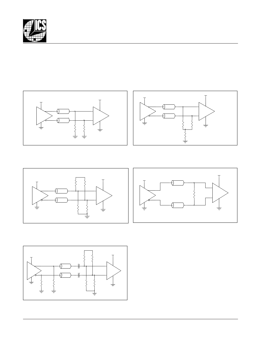
The CLK /nCLK accepts LVDS, LVPECL, LVHSTL, SSTL, HCSL
and other differential signals. Both V
SWING
and V
OH
must meet the
V
PP
and V
CMR
input requirements. Figures 5A to 5E show inter-
face examples for the HiPerClockS CLK/nCLK input driven by
the most common driver types. The input interfaces suggested
F
IGURE
5A. H
I
P
ER
C
LOCK
S CLK/nCLK I
NPUT
D
RIVEN
BY
ICS H
I
P
ER
C
LOCK
S LVHSTL D
RIVER
here are examples only. Please consult with the vendor of the
driver component to confirm the driver termination requirements.
For example in
Figure 5A, the input termination applies for ICS
HiPerClockS LVHSTL drivers. If you are using an LVHSTL driver
from another vendor, use their termination recommendation.
1.8V
R2
50
Input
LVHSTL Driver
ICS
HiPerClockS
R1
50
LVHSTL
3.3V
Zo = 50 Ohm
Zo = 50 Ohm
HiPerClockS
CLK
nCLK
Zo = 50 Ohm
R1
100
3.3V
LVDS_Driv er
Zo = 50 Ohm
Receiv er
CLK
nCLK
3.3V
F
IGURE
5E. H
I
P
ER
C
LOCK
S CLK/nCLK I
NPUT
D
RIVEN
BY
3.3V LVPECL D
RIVER
WITH
AC C
OUPLE
Zo = 50 Ohm
R3
125
HiPerClockS
CLK
nCLK
3.3V
R5
100 - 200
3.3V
R2
84
3.3V
R6
100 - 200
Input
R5,R6 locate near the driver pin.
Zo = 50 Ohm
R1
84
R4
125
C2
LVPECL
C1

843002AKI-40
www.icst.com/products/hiperclocks.html
REV. A JUNE 22, 2005
16
Integrated
Circuit
Systems, Inc.
ICS843002I-40
175MH
Z
, F
EMTO
C
LOCKS
TM VCXO B
ASED
SONET/SDH J
ITTER
A
TTENUATOR
PRELIMINARY
S
INGLE
E
NDED
C
LOCK
I
NPUT
I
NTERFACE
When using a LVCMOS or LVTTL clock driver, the clock
input is connected to the CLKx (CLK0 or CLK1) input pin. The
nCLKx (nCLK0 or nCLK1) pin is left unconnected. To help
reduce interference with the internal VCO circuits, an external
resistor can be placed in series with the clock signal right
near the CLKx input pin. Combined with the input pin
capacitance, this resistor acts as a low pass signal filter.
The typical value for this optional series filter resistor is 100
.
This will lower both the amplitude and edge rate of the clock
input signal. In the case of a very short clock trace a series
termination resistor may not be needed.
F
IGURE
6. S
INGLE
-E
NDED
C
LOCK
I
NPUT
I
NTERFACE
3.3V
CLK
nCLK
3.3V
(no connection)
Differential
Input Stage
LVTTL or
LVCMOS
Series
Termination
Optional
Series
Filter
Resistor
nCLKx
CLKx
Internal Device Circuitry
External Circuitry
50k
50k
50k

843002AKI-40
www.icst.com/products/hiperclocks.html
REV. A JUNE 22, 2005
17
Integrated
Circuit
Systems, Inc.
ICS843002I-40
175MH
Z
, F
EMTO
C
LOCKS
TM VCXO B
ASED
SONET/SDH J
ITTER
A
TTENUATOR
PRELIMINARY
P
OWER
C
ONSIDERATIONS
This section provides information on power dissipation and junction temperature for the ICS843002I-40.
Equations and example calculations are also provided.
1. Power Dissipation.
The total power dissipation for the ICS843002I-40 is the sum of the core power plus the power dissipated in the load(s).
The following is the power dissipation for V
CC
= 3.3V + 5% = 3.465V, which gives worst case results.
NOTE: Please refer to Section 3 for details on calculating power dissipated in the load.
∑
Power (core)
MAX
= V
CC_MAX
* I
EE_MAX
= 3.465V * 175mA = 606.375mW
∑
Power (outputs)
MAX
= 30mW/Loaded Output pair
If all outputs are loaded, the total power is 2 * 30mW = 120mW
Total Power
_MAX
(3.465V, with all outputs switching) = 606.375mW + 60mW = 666.38mW
2. Junction Temperature.
Junction temperature, Tj, is the temperature at the junction of the bond wire and bond pad and directly affects the reliability of the
device. The maximum recommended junction temperature for HiPerClockS
TM
devices is 125∞C.
The equation for Tj is as follows: Tj =
JA
* Pd_total + T
A
Tj = Junction Temperature
JA
= Junction-to-Ambient Thermal Resistance
Pd_total = Total Device Power Dissipation (example calculation is in section 1 above)
T
A
= Ambient Temperature
In order to calculate junction temperature, the appropriate junction-to-ambient thermal resistance
JA
must be used. Assuming an
air flow of 0 linear feet per minute and a multi-layer board, the appropriate value is 34.8∞C/W per Table 7 below.
Therefore, Tj for an ambient temperature of 85∞C with all outputs switching is:
85∞C + 0.666W * 34.8∞C/W = 108.2∞C. This is well below the limit of 125∞C.
This calculation is only an example. Tj will obviously vary depending on the number of loaded outputs, supply voltage, air flow,
and the type of board (single layer or multi-layer).
T
ABLE
7. T
HERMAL
R
ESISTANCE
JA
FOR
32-
PIN
VFQFN, F
ORCED
C
ONVECTION
JA
vs. Air Flow (Linear Feet per Minute)
0
Multi-Layer PCB, JEDEC Standard Test Boards
34.8∞C/W
843002AKI-40
www.icst.com/products/hiperclocks.html
REV. A JUNE 22, 2005
18
Integrated
Circuit
Systems, Inc.
ICS843002I-40
175MH
Z
, F
EMTO
C
LOCKS
TM VCXO B
ASED
SONET/SDH J
ITTER
A
TTENUATOR
PRELIMINARY
3. Calculations and Equations.
The purpose of this section is to derive the power dissipated into the load.
LVPECL output driver circuit and termination are shown in
Figure 7.
T
o calculate worst case power dissipation into the load, use the following equations which assume a 50
load, and a termination
voltage of V
CCO
- 2V.
∑
For logic high, V
OUT
= V
OH_MAX
= V
CCO_MAX
≠ 0.9V
(V
CCO_MAX
- V
OH_MAX
) = 0.9V
∑
For logic low, V
OUT
= V
OL_MAX
= V
CCO_MAX
≠ 1.7V
(V
CCO_MAX
- V
OL_MAX
) = 1.7V
Pd_H is power dissipation when the output drives high.
Pd_L is the power dissipation when the output drives low.
Pd_H = [(V
OH_MAX
≠ (V
CCO_MAX
- 2V))/R
L
] * (V
CCO_MAX
- V
OH_MAX
) = [(2V - (V
CCO_MAX
- V
OH_MAX
))/R
L
] * (V
CCO_MAX
- V
OH_MAX
) =
[(2V - 0.9V)/50
) * 0.9V = 19.8mW
Pd_L = [(V
OL_MAX
≠ (V
CCO_MAX
- 2V))/R
L
] * (V
CCO_MAX
- V
OL_MAX
) = [(2V - (V
CCO_MAX
- V
OL_MAX
))/R
L
] * (V
CCO_MAX
- V
OL_MAX
) =
[(2V - 1.7V)/50
) * 1.7V = 10.2mW
Total Power Dissipation per output pair = Pd_H + Pd_L = 30mW
F
IGURE
7. LVPECL D
RIVER
C
IRCUIT
AND
T
ERMINATION
Q1
V
OUT
V
CCO
R L
50
V
CCO
- 2V

843002AKI-40
www.icst.com/products/hiperclocks.html
REV. A JUNE 22, 2005
19
Integrated
Circuit
Systems, Inc.
ICS843002I-40
175MH
Z
, F
EMTO
C
LOCKS
TM VCXO B
ASED
SONET/SDH J
ITTER
A
TTENUATOR
PRELIMINARY
R
ELIABILITY
I
NFORMATION
T
RANSISTOR
C
OUNT
The transistor count for ICS843002I-40 is: 5536
T
ABLE
8.
JA
VS
. A
IR
F
LOW
T
ABLE
FOR
A
32 L
EAD
VFQFN
JA
vs. Air Flow (Linear Feet per Minute)
0
Multi-Layer PCB, JEDEC Standard Test Boards
34.8∞C/W
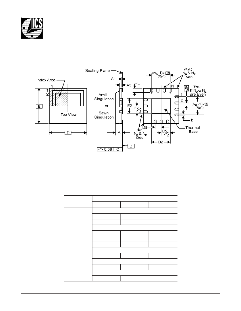
843002AKI-40
www.icst.com/products/hiperclocks.html
REV. A JUNE 22, 2005
20
Integrated
Circuit
Systems, Inc.
ICS843002I-40
175MH
Z
, F
EMTO
C
LOCKS
TM VCXO B
ASED
SONET/SDH J
ITTER
A
TTENUATOR
PRELIMINARY
P
ACKAGE
O
UTLINE
- K S
UFFIX
FOR
A
32 L
EAD
VFQFN
T
ABLE
9. P
ACKAGE
D
IMENSIONS
Reference Document: JEDEC Publication 95, MO-220
N
O
I
T
A
I
R
A
V
C
E
D
E
J
S
R
E
T
E
M
I
L
L
I
M
N
I
S
N
O
I
S
N
E
M
I
D
L
L
A
L
O
B
M
Y
S
2
-
D
H
H
V
M
U
M
I
N
I
M
L
A
N
I
M
O
N
M
U
M
I
X
A
M
N
2
3
A
0
8
.
0
-
-
0
0
.
1
1
A
0
-
-
5
0
.
0
3
A
.
f
e
R
5
2
.
0
b
8
1
.
0
5
2
.
0
0
3
.
0
N
D
8
N
E
8
D
C
I
S
A
B
0
0
.
5
2
D
5
2
.
1
5
2
.
2
5
2
.
3
E
C
I
S
A
B
0
0
.
5
2
E
5
2
.
1
5
2
.
2
5
2
.
3
e
C
I
S
A
B
0
5
.
0
L
0
3
.
0
0
4
.
0
0
5
.
0

843002AKI-40
www.icst.com/products/hiperclocks.html
REV. A JUNE 22, 2005
21
Integrated
Circuit
Systems, Inc.
ICS843002I-40
175MH
Z
, F
EMTO
C
LOCKS
TM VCXO B
ASED
SONET/SDH J
ITTER
A
TTENUATOR
PRELIMINARY
T
ABLE
10. O
RDERING
I
NFORMATION
While the information presented herein has been checked for both accuracy and reliability, Integrated Circuit Systems, Incorporated (ICS) assumes no responsibility for either its use
or for infringement of any patents or other rights of third parties, which would result from its use. No other circuits, patents, or licenses are implied. This product is intended for use
in normal commercial and industrial applications. Any other applications such as those requiring high reliability or other extraordinary environmental requirements are not
recommended without additional processing by ICS. ICS reserves the right to change any circuitry or specifications without notice. ICS does not authorize or warrant any ICS product
for use in life support devices or critical medical instruments.
The aforementioned trademarks, HiPerClockS and F
EMTO
C
LOCKS
are trademarks of Integrated Circuit Systems, Inc. or its subsidiaries in the United States and/or other countries.
r
e
b
m
u
N
r
e
d
r
O
/
t
r
a
P
g
n
i
k
r
a
M
e
g
a
k
c
a
P
g
n
i
g
a
k
c
a
P
g
n
i
p
p
i
h
S
e
r
u
t
a
r
e
p
m
e
T
0
4
-
I
K
A
2
0
0
3
4
8
S
C
I
0
4
A
2
0
0
3
4
S
C
I
N
F
Q
F
V
d
a
e
L
2
3
y
a
r
t
C
∞
5
8
o
t
C
∞
0
4
-
T
0
4
-
I
K
A
2
0
0
3
4
8
S
C
I
0
4
A
2
0
0
3
4
S
C
I
N
F
Q
F
V
d
a
e
L
2
3
l
e
e
r
&
e
p
a
t
0
0
5
2
C
∞
5
8
o
t
C
∞
0
4
-