Document Outline
- General Description
- Features
- Pin Assignment
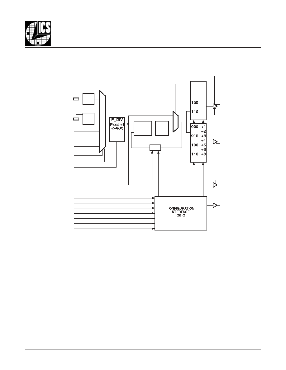
- Block Diagram
- Functional Description
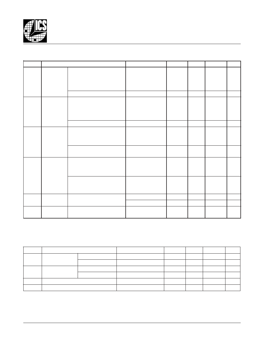
- Parallel & Serial Load Operations Diagram
- Pin Descriptions
- Pin Descriptions continued
- Pin Characteristics
- Parallel & Serial Mode Function Table
- Programmable VCO Frequency Function Table
- Programmable Output Divider Function Table
- Absolute Maximum Ratings
- Power Supply DC Characteristics
- LVCMOS DC Characteristics
- Differential DC Characteristics
- LVPECL DC Characteristics
- Input Frequency Characteristics
- Crystal Characteristics
- 3.3V AC Characteristics
- 3.3V/2.5V AC Characteristics
- 3.3V/3.3V/2.5V or 3.3V/2.5V/3.3V AC Characteristics
- Typical Phase Noise Plot
- Parameter Measurement Information
- Application Information
- Power Supply Filtering Techniques
- Wiring the Differential Input to Accept Single Ended LVCMOS/LVTTL Levels
- Crystal Input Interface
- Differential Clock Input Interface
- Termination for 3.3V LVPECL Output
- Recommendations for Unused Input and Output Pins
- Termination for 2.5V LVPECL Output
- Power Considerations
- Power Dissipation
- Junction Temperature
- Thermal Resistance
- Calculations & Equations
- LVPECL Driver Circuit & Termination
- Reliability Information
- Transistor Count
- Package Outline
- Package Dimensions
- Ordering Information
843034AY-01
www.icst.com/products/hiperclocks.html
REV. C NOVEMBER 28, 2005
1
Integrated
Circuit
Systems, Inc.
ICS843034-01
F
EMTO
C
LOCKS
TM
M
ULTI
-R
ATE
LVPECL F
REQUENCY
S
YNTHESIZER
PRELIMINARY
G
ENERAL
D
ESCRIPTION
The ICS843034-01 is a general purpose, low
phase noise LVPECL synthesizer which can
generate frequencies for a wide variety of
applications. The ICS843034-01 has a 4:1
input Multiplexer from which the following
inputs can be selected: 1 differential input, 1
single-ended input, or one of two crystal oscillators,
thus making the device ideal for frequency translation or
generation. Each differential LVPECL output pair has an
output divider which can be independently set so that two
different frequencies can be generated. Additionally, each
LVPECL output pair has a dedicated power supply pin so
the outputs can run at 3.3V or 2.5V. The ICS843034-01
also supplies a buffered copy of the reference clock or
crystal frequency on the single-ended REF_CLK pin which
can be enabled or disabled (disabled by default). The output
frequency can be programmed using either a serial or
parallel programming interface.
The ICS843034-01 has excellent <1ps phase jitter
performance over the 637kHz - 5MHz integration range, thus
making it suitable for use in Fibre Channel, SONET, and
Ethernet/1Gb Ethernet applications.
Example applications include systems which must support
both FEC and non FEC rates. In 10Gb Fibre Channel, for
example, you can use a 25.5MHz crystal to generate a
159.375MHz reference clock, and then switch to a
20.544MHz crystal to generate 164.355MHz for 66/64 FEC.
Other applications could include supporting both Ethernet
frequencies and SONET frequencies in an application. When
Ethernet frequencies are needed, a 25MHz crystal can be
used and when SONET frequencies are needed, the input
MUX can be switched to select a 38.88MHz Crystal.
F
EATURES
� Dual differential 3.3V LVPECL outputs which can be set
independently for either 3.3V or 2.5V
� 4:1 Input Mux:
1 differential input
1 single-ended input
2 crystal oscillator interfaces
� CLK, nCLK pair can accept the following differential
input levels: LVPECL, LVDS, LVHSTL, HCSL, SSTL
� TEST_CLK accepts LVCMOS or LVTTL input levels
� Output frequency range: 30.625MHz to 640MHz
� Crystal input frequency range: 12MHz to 40MHz
� VCO range: 490MHz to 640MHz
� Parallel or serial interface for programming feedback divider
and output dividers
� RMS phase jitter at 106.25MHz, using a 25.5MHz crystal
(637kHz to 5MHz): 0.61ps (typical)
� Supply voltage modes:
LVPECL outputs (core/outputs):
3.3V/3.3V
3.3V/2.5V
REF_CLK output (core/outputs):
3.3V/3.3V
3.3V/2.5V
� 0�C to 70�C ambient operating temperature
� Available in both standard and lead-free RoHS-compliant
packages
HiPerClockSTM
ICS
P
IN
A
SSIGNMENT
48 47 46 45 44 43 42 41 40 39 38 37
13 14 15 16 17 18 19 20 21 22 23 24
1
2
3
4
5
6
7
8
9
10
11
12
36
35
34
33
32
31
30
29
28
27
26
25
M8
NB0
NB1
NB2
OE_REF
OE_A
OE_B
V
CC
NA0
NA1
NA2
V
EE
XTAL_OUT1
XTAL_IN1
XTAL_OUT0
XTAL_IN0
TEST_CLK
SEL1
SEL0
V
CCA
S_LOAD
S_DATA
S_CLOCK
MR
CLK
nCLK
nP_LOAD
VCO_SEL
M0
M1
M2
M3
M4
M5
M6
M7
ICS843034-01
48-Pin LQFP
7mm x 7mm x 1.4mm
package body
Y Package
Top View
V
EE
P_DIV
V
CCO
_
REF
REF_CLK
V
CCO
_
B
nFOUTB0
FOUTB0
V
CCO
_
A
nFOUT
A0
FOUT
A
0
V
CC
TEST
The Preliminary Information presented herein represents a product in prototyping or pre-production. The noted characteristics are based on initial
product characterization. Integrated Circuit Systems, Incorporated (ICS) reserves the right to change any circuitry or specifications without notice.
843034AY-01
www.icst.com/products/hiperclocks.html
REV. C NOVEMBER 28, 2005
2
Integrated
Circuit
Systems, Inc.
ICS843034-01
F
EMTO
C
LOCKS
TM
M
ULTI
-R
ATE
LVPECL F
REQUENCY
S
YNTHESIZER
PRELIMINARY
OSC
C
I
L
�M
0
0
1
001
011
101
111
�16
�
000
�1
001
�2
010
�3
011
�4
�5
101
�6
�8
111
�16
�
OSC
P
HASE
D
ETECTOR
VCO
0 0
0 1
1 0
1 1
1
� 4
0
�8
FOUTA0
nFOUTA0
FOUTB0
nFOUTB0
REF_CLK
TEST
V
CCO_REF
V
CCO_A
V
CCO_B
OE_A
VCO_SEL
XTAL_IN0
XTAL_OUT0
XTAL_IN1
XTAL_OUT1
CLK
nCLK
TEST_CLK
SEL1
SEL0
P_DIV
OE_B
MR
OE_REF
S_LOAD
S_DATA
S_CLOCK
nP_LOAD
M8:M0
NA2:NA0
NB2:NB0
B
LOCK
D
IAGRAM

843034AY-01
www.icst.com/products/hiperclocks.html
REV. C NOVEMBER 28, 2005
3
Integrated
Circuit
Systems, Inc.
ICS843034-01
F
EMTO
C
LOCKS
TM
M
ULTI
-R
ATE
LVPECL F
REQUENCY
S
YNTHESIZER
PRELIMINARY
Nx bits can be hardwired to set the M divider and Nx output
divider to a specific default state that will automatically occur
during power-up. The TEST output is LOW when operating in
the parallel input mode. The relationship between the VCO fre-
quency, the crystal frequency and the M divider is defined as
follows:
The M value and the required values of M0 through M5 are shown
in Table 3B to program the VCO Frequency Function Table.
Valid M values for which the PLL will achieve lock for a 25MHz
reference are defined as 20
M 25. The frequency out is de-
fined as follows:
Serial operation occurs when nP_LOAD is HIGH and S_LOAD
is LOW. The shift register is loaded by sampling the S_DATA
bits with the rising edge of S_CLOCK. The contents of the
shift register are loaded into the M divider and Nx output di-
vider when S_LOAD transitions from LOW-to-HIGH. The M
divide and Nx output divide values are latched on the HIGH-
to-LOW transition of S_LOAD. If S_LOAD is held HIGH, data
at the S_DATA input is passed directly to the M divider and Nx
output divider on each rising edge of S_CLOCK. The serial
mode can be used to program the M and Nx bits and test bits
T1 and T0. The internal registers T0 and T1 determine the state
of the TEST output as follows:
F
UNCTIONAL
D
ESCRIPTION
NOTE: The functional description that follows describes op-
eration using a 25MHz crystal. Valid PLL loop divider values
for different crystal or input frequencies are defined in the In-
put Frequency Characteristics, Table 5, NOTE 1.
The ICS843034-01 features a fully integrated PLL and there-
fore requires no external components for setting the loop band-
width. A fundamental crystal is used as the input to the on-
chip oscillator. The output of the oscillator is fed into the phase
detector. A 25MHz crystal provides a 25MHz phase detector
reference frequency. The VCO of the PLL operates over a
range of 490MHz to 640MHz. The output of the M divider is
also applied to the phase detector.
The phase detector and the M divider force the VCO output fre-
quency to be M times the reference frequency by adjusting the
VCO control voltage. Note that for some values of M (either too
high or too low), the PLL will not achieve lock. The output of the
VCO is scaled by a divider prior to being sent to each of the LVPECL
output buffers. The divider provides a 50% output duty cycle.
The ICS843034-01 supports either serial or parallel program-
ming modes to program the M feedback divider and N output
divider. The input divider P can only be changed using the P_DIV
pin. It cannot be changed from the default
�1 setting using the
serial interface.
Figure 1
shows the timing diagram for each mode.
In parallel mode, the nP_LOAD input is initially LOW. The data
on the M, NA, and NB inputs are passed directly to the M di-
vider and both N output dividers. On the LOW-to-HIGH transi-
tion of the nP_LOAD input, the data is latched and the M and N
dividers remain loaded until the next LOW transition on
nP_LOAD or until a serial event occurs. As a result, the M and
T1
T0
TEST Output
0
0
LOW
0
1
S_Data, Shift Register Output
1
0
Output of M divider
1
1
CMOS Fout A0
F
IGURE
1. P
ARALLEL
& S
ERIAL
L
OAD
O
PERATIONS
T 1
T0
NB2
NB1 NB0
NA2
NA1
NA0
M8
M7
M6
M5
M4
M3
M2
M1
M 0
S_CLOCK
S_DATA
S_LOAD
nP_LOAD
M0:M8, P_DIV,
NA0:NA2, NB0:NB2
nP_LOAD
fVCO = fxtal x M
P
FOUT = fVCO = fxtal x M
N
N x P
S
ERIAL
L
OADING
P
ARALLEL
L
OADING
M, N, P
t
S
t
S
t
H
t
S
t
H
Time
S_LOAD
843034AY-01
www.icst.com/products/hiperclocks.html
REV. C NOVEMBER 28, 2005
4
Integrated
Circuit
Systems, Inc.
ICS843034-01
F
EMTO
C
LOCKS
TM
M
ULTI
-R
ATE
LVPECL F
REQUENCY
S
YNTHESIZER
PRELIMINARY
T
ABLE
1. P
IN
D
ESCRIPTIONS
r
e
b
m
u
N
e
m
a
N
e
p
y
T
n
o
i
t
p
i
r
c
s
e
D
1
8
M
t
u
p
n
I
n
w
o
d
ll
u
P
D
A
O
L
_
P
n
f
o
n
o
i
t
i
s
n
r
t
H
G
I
H
-
o
t
-
W
O
L
n
o
d
e
h
c
t
a
l
a
t
a
D
.
t
u
p
n
i
r
e
d
i
v
i
d
M
.
s
l
e
v
e
l
c
a
f
r
e
t
n
i
L
T
T
V
L
/
S
O
M
C
V
L
.
t
u
p
n
i
3
,
2
1
B
N
,
0
B
N
t
u
p
n
I
p
u
ll
u
P
,
C
3
e
l
b
a
T
n
i
d
e
n
i
f
e
d
s
a
e
u
l
a
v
r
e
d
i
v
i
d
t
u
p
t
u
o
s
e
n
i
m
r
e
t
e
D
.
s
l
e
v
e
l
e
c
a
f
r
e
t
n
i
L
T
T
V
L
/
S
O
M
C
V
L
.
e
l
b
a
T
n
o
i
t
c
n
u
F
4
2
B
N
t
u
p
n
I
n
w
o
d
ll
u
P
5
F
E
R
_
E
O
t
u
p
n
I
n
w
o
d
ll
u
P
.
t
u
p
t
u
o
K
L
C
_
F
E
R
f
o
g
n
il
b
a
s
i
d
d
n
a
g
n
il
b
a
n
e
s
l
o
r
t
n
o
C
.
e
l
b
a
n
e
t
u
p
t
u
O
.
s
l
e
v
e
l
e
c
a
f
r
e
t
n
i
L
T
T
V
L
/
S
O
M
C
V
L
6
A
_
E
O
t
u
p
n
I
p
u
ll
u
P
,
0
A
T
U
O
F
f
o
g
n
il
b
a
s
i
d
d
n
a
g
n
il
b
a
n
e
s
l
o
r
t
n
o
C
.
e
l
b
a
n
e
t
u
p
t
u
O
.
s
l
e
v
e
l
e
c
a
f
r
e
t
n
i
L
T
T
V
L
/
S
O
M
C
V
L
.
s
t
u
p
t
u
o
0
A
T
U
O
F
n
7
B
_
E
O
t
u
p
n
I
p
u
ll
u
P
,
0
B
T
U
O
F
f
o
g
n
il
b
a
s
i
d
d
n
a
g
n
il
b
a
n
e
s
l
o
r
t
n
o
C
.
e
l
b
a
n
e
t
u
p
t
u
O
.
s
l
e
v
e
l
e
c
a
f
r
e
t
n
i
L
T
T
V
L
/
S
O
M
C
V
L
.
s
t
u
p
t
u
o
0
B
T
U
O
F
n
4
1
,
8
V
C
C
r
e
w
o
P
.
s
n
i
p
y
l
p
p
u
s
e
r
o
C
0
1
,
9
1
A
N
,
0
A
N
t
u
p
n
I
p
u
ll
u
P
,
C
3
e
l
b
a
T
n
i
d
e
n
i
f
e
d
s
a
e
u
l
a
v
r
e
d
i
v
i
d
t
u
p
t
u
o
s
e
n
i
m
r
e
t
e
D
.
s
l
e
v
e
l
e
c
a
f
r
e
t
n
i
L
T
T
V
L
/
S
O
M
C
V
L
.
e
l
b
a
T
n
o
i
t
c
n
u
F
1
1
2
A
N
t
u
p
n
I
n
w
o
d
ll
u
P
4
2
,
2
1
V
E
E
r
e
w
o
P
.
s
n
i
p
y
l
p
p
u
s
e
v
i
t
a
g
e
N
3
1
T
S
E
T
t
u
p
t
u
O
.
n
o
i
t
a
r
e
p
o
f
o
e
d
o
m
l
a
i
r
e
s
e
h
t
n
i
E
V
I
T
C
A
s
i
h
c
i
h
w
t
u
p
t
u
o
t
s
e
T
.
e
d
o
m
l
e
ll
a
r
a
p
n
i
W
O
L
n
e
v
i
r
d
t
u
p
t
u
O
.
s
l
e
v
e
l
e
c
a
f
r
e
t
n
i
L
T
T
V
L
/
S
O
M
C
V
L
6
1
,
5
1
,
0
A
T
U
O
F
0
A
T
U
O
F
n
t
u
p
t
u
O
.
s
l
e
v
e
l
e
c
a
f
r
e
t
n
i
L
C
E
P
V
L
.
r
e
z
i
s
e
h
t
n
y
s
e
h
t
r
o
f
t
u
p
t
u
o
l
a
i
t
n
e
r
e
f
f
i
D
7
1
V
A
_
O
C
C
r
e
w
o
P
.
0
A
T
U
O
F
n
,
0
A
T
U
O
F
r
o
f
n
i
p
y
l
p
p
u
s
t
u
p
t
u
O
9
1
,
8
1
,
0
B
T
U
O
F
0
B
T
U
O
F
n
t
u
p
t
u
O
.
s
l
e
v
e
l
e
c
a
f
r
e
t
n
i
L
C
E
P
V
L
.
r
e
z
i
s
e
h
t
n
y
s
e
h
t
r
o
f
t
u
p
t
u
o
l
a
i
t
n
e
r
e
f
f
i
D
0
2
V
B
_
O
C
C
r
e
w
o
P
.
0
B
T
U
O
F
n
,
0
B
T
U
O
F
r
o
f
n
i
p
y
l
p
p
u
s
t
u
p
t
u
O
1
2
K
L
C
_
F
E
R
t
u
p
t
u
O
.
s
l
e
v
e
l
e
c
a
f
r
e
t
n
i
L
T
T
V
L
/
S
O
M
C
V
L
.
t
u
p
t
u
o
k
c
o
l
c
e
c
n
e
r
e
f
e
R
2
2
V
F
E
R
_
O
C
C
r
e
w
o
P
.
K
L
C
_
F
E
R
r
o
f
n
i
p
y
l
p
p
u
s
t
u
p
t
u
O
3
2
V
I
D
_
P
t
u
p
n
I
/
p
u
ll
u
P
n
w
o
d
ll
u
P
=
1
,
)
t
l
u
a
f
e
d
(
1
�
=
t
a
o
l
F
.
t
c
e
l
e
s
e
d
i
v
i
d
t
u
p
n
I
�
.
8
�
=
0
,
4
.
s
l
e
v
e
l
e
c
a
f
r
e
t
n
i
L
T
T
V
L
/
S
O
M
C
V
L
5
2
R
M
t
u
p
n
I
n
w
o
d
ll
u
P
l
a
n
r
e
t
n
i
e
h
t
s
e
c
r
o
f
,
H
G
I
H
c
i
g
o
l
n
e
h
W
.
t
e
s
e
R
r
e
t
s
a
M
h
g
i
H
e
v
i
t
c
A
e
h
t
d
n
a
w
o
l
o
g
o
t
x
T
U
O
F
s
t
u
p
t
u
o
e
u
r
t
e
h
t
g
n
i
s
u
a
c
t
e
s
e
r
e
r
a
s
r
e
d
i
v
i
d
l
a
n
r
e
t
n
i
e
h
t
,
W
O
L
c
i
g
o
l
n
e
h
W
.
h
g
i
h
o
g
o
t
x
T
U
O
F
n
s
t
u
p
t
u
o
d
e
t
r
e
v
n
i
t
o
n
s
e
o
d
R
M
f
o
n
o
i
t
r
e
s
s
A
.
d
e
l
b
a
n
e
e
r
a
s
t
u
p
t
u
o
e
h
t
d
n
a
s
r
e
d
i
v
i
d
.
s
l
e
v
e
l
e
c
a
f
r
e
t
n
i
L
T
T
V
L
/
S
O
M
C
V
L
.
s
e
u
l
a
v
T
d
n
a
,
N
,
M
d
e
d
a
o
l
t
c
e
f
f
a
6
2
K
C
O
L
C
_
S
t
u
p
n
I
n
w
o
d
ll
u
P
r
e
t
s
i
g
e
r
t
f
i
h
s
e
h
t
o
t
n
i
t
u
p
n
i
A
T
A
D
_
S
t
a
t
n
e
s
e
r
p
a
t
a
d
l
a
i
r
e
s
n
i
s
k
c
o
l
C
.
s
l
e
v
e
l
e
c
a
f
r
e
t
n
i
L
T
T
V
L
/
S
O
M
C
V
L
.
K
C
O
L
C
_
S
f
o
e
g
d
e
g
n
i
s
i
r
e
h
t
n
o
7
2
A
T
A
D
_
S
t
u
p
n
I
n
w
o
d
ll
u
P
e
g
d
e
g
n
i
s
i
r
e
h
t
n
o
d
e
l
p
m
a
s
a
t
a
D
.
t
u
p
n
i
l
a
i
r
e
s
r
e
t
s
i
g
e
r
t
f
i
h
S
.
s
l
e
v
e
l
e
c
a
f
r
e
t
n
i
L
T
T
V
L
/
S
O
M
C
V
L
.
K
C
O
L
C
_
S
f
o
8
2
D
A
O
L
_
S
t
u
p
n
I
n
w
o
d
ll
u
P
.
s
r
e
d
i
v
i
d
e
h
t
o
t
n
i
r
e
t
s
i
g
e
r
t
f
i
h
s
m
o
r
f
a
t
a
d
f
o
n
o
i
t
i
s
n
a
r
t
s
l
o
r
t
n
o
C
.
s
l
e
v
e
l
e
c
a
f
r
e
t
n
i
L
T
T
V
L
/
S
O
M
C
V
L
9
2
V
A
C
C
r
e
w
o
P
.
n
i
p
y
l
p
p
u
s
g
o
l
a
n
A
1
3
,
0
3
1
L
E
S
,
0
L
E
S
t
u
p
n
I
n
w
o
d
ll
u
P
.
s
l
e
v
e
l
e
c
a
f
r
e
t
n
i
L
T
T
V
L
/
S
O
M
C
V
L
.
s
t
u
p
n
i
t
c
e
l
e
s
k
c
o
l
C
2
3
K
L
C
_
T
S
E
T
t
u
p
n
I
n
w
o
d
ll
u
P
.
s
l
e
v
e
l
e
c
a
f
r
e
t
n
i
L
T
T
V
L
/
S
O
M
C
V
L
.
t
u
p
n
i
k
c
o
l
c
t
s
e
T
4
3
,
3
3
,
0
N
I
_
L
A
T
X
0
T
U
O
_
L
A
T
X
t
u
p
n
I
.
e
c
a
f
r
e
t
n
i
r
o
t
a
ll
i
c
s
o
l
a
t
s
y
r
C
6
3
,
5
3
,
1
N
I
_
L
A
T
X
1
T
U
O
_
L
A
T
X
t
u
p
n
I
.
e
c
a
f
r
e
t
n
i
r
o
t
a
ll
i
c
s
o
l
a
t
s
y
r
C
7
3
K
L
C
t
u
p
n
I
n
w
o
d
ll
u
P
.
t
u
p
n
i
k
c
o
l
c
l
a
i
t
n
e
r
e
f
f
i
d
g
n
i
t
r
e
v
n
i
-
n
o
N
8
3
K
L
C
n
t
u
p
n
I
/
p
u
ll
u
P
n
w
o
d
ll
u
P
V
.
t
u
p
n
i
k
c
o
l
c
l
a
i
t
n
e
r
e
f
f
i
d
g
n
i
t
r
e
v
n
I
C
C
.
g
n
i
t
a
o
l
f
t
f
e
l
n
e
h
w
t
l
u
a
f
e
d
2
/
.
.
.
e
g
a
p
t
x
e
n
n
o
d
e
u
n
i
t
n
o
C

843034AY-01
www.icst.com/products/hiperclocks.html
REV. C NOVEMBER 28, 2005
5
Integrated
Circuit
Systems, Inc.
ICS843034-01
F
EMTO
C
LOCKS
TM
M
ULTI
-R
ATE
LVPECL F
REQUENCY
S
YNTHESIZER
PRELIMINARY
T
ABLE
2. P
IN
C
HARACTERISTICS
l
o
b
m
y
S
r
e
t
e
m
a
r
a
P
s
n
o
i
t
i
d
n
o
C
t
s
e
T
m
u
m
i
n
i
M
l
a
c
i
p
y
T
m
u
m
i
x
a
M
s
t
i
n
U
C
N
I
e
c
n
a
t
i
c
a
p
a
C
t
u
p
n
I
4
F
p
R
P
U
L
L
U
P
r
o
t
s
i
s
e
R
p
u
ll
u
P
t
u
p
n
I
1
5
k
R
N
W
O
D
L
L
U
P
r
o
t
s
i
s
e
R
n
w
o
d
ll
u
P
t
u
p
n
I
1
5
k
R
T
U
O
e
c
n
a
d
e
p
m
I
t
u
p
t
u
O
5
7
2
1
r
e
b
m
u
N
e
m
a
N
e
p
y
T
n
o
i
t
p
i
r
c
s
e
D
9
3
D
A
O
L
_
P
n
t
u
p
n
I
n
w
o
d
ll
u
P
s
i
0
M
:
5
M
t
a
t
n
e
s
e
r
p
a
t
a
d
n
e
h
w
s
e
n
i
m
r
e
t
e
D
.
t
u
p
n
i
d
a
o
l
l
e
ll
a
r
a
P
d
n
a
0
A
N
:
2
A
N
t
a
t
n
e
s
e
r
p
a
t
a
d
n
e
h
w
d
n
a
,
r
e
d
i
v
i
d
M
o
t
n
i
d
e
d
a
o
l
.
s
r
e
d
i
v
i
d
t
u
p
t
u
o
N
e
h
t
o
t
n
i
d
e
d
a
o
l
s
i
0
B
N
:
2
B
N
.
s
l
e
v
e
l
e
c
a
f
r
e
t
n
i
L
T
T
V
L
/
S
O
M
C
V
L
0
4
L
E
S
_
O
C
V
t
u
p
n
I
p
u
ll
u
P
.
e
d
o
m
s
s
a
p
y
b
r
o
L
L
P
n
i
s
i
r
e
z
i
s
e
h
t
n
y
s
r
e
h
t
e
h
w
s
e
n
i
m
r
e
t
e
D
.
s
l
e
v
e
l
e
c
a
f
r
e
t
n
i
L
T
T
V
L
/
S
O
M
C
V
L
,
3
4
,
2
4
,
1
4
8
4
,
7
4
,
5
4
,
4
4
,
2
M
,
1
M
,
0
M
7
M
,
6
M
,
4
M
,
3
M
t
u
p
n
I
n
w
o
d
ll
u
P
n
o
i
t
i
s
n
a
r
t
H
G
I
H
-
o
t
-
W
O
L
n
o
d
e
h
c
t
a
l
a
t
a
D
.
s
t
u
p
n
i
r
e
d
i
v
i
d
M
.
s
l
e
v
e
l
e
c
a
f
r
e
t
n
i
L
T
T
V
L
/
S
O
M
C
V
L
.
t
u
p
n
i
D
A
O
L
_
P
n
f
o
6
4
5
M
t
u
p
n
I
p
u
ll
u
P
:
E
T
O
N
p
u
ll
u
P
d
n
a
n
w
o
d
ll
u
P
.
s
e
u
l
a
v
l
a
c
i
p
y
t
r
o
f
,
s
c
i
t
s
i
r
e
t
c
a
r
a
h
C
n
i
P
,
2
e
l
b
a
T
e
e
S
.
s
r
o
t
s
i
s
e
r
t
u
p
n
i
l
a
n
r
e
t
n
i
o
t
r
e
f
e
r
843034AY-01
www.icst.com/products/hiperclocks.html
REV. C NOVEMBER 28, 2005
6
Integrated
Circuit
Systems, Inc.
ICS843034-01
F
EMTO
C
LOCKS
TM
M
ULTI
-R
ATE
LVPECL F
REQUENCY
S
YNTHESIZER
PRELIMINARY
T
ABLE
3A. P
ARALLEL
AND
S
ERIAL
M
ODE
F
UNCTION
T
ABLE
s
t
u
p
n
I
s
n
o
i
t
i
d
n
o
C
R
M
D
A
O
L
_
P
n
M
N
D
A
O
L
_
S
K
C
O
L
C
_
S
A
T
A
D
_
S
H
X
X
X
X
X
X
.
W
O
L
s
t
u
p
t
u
o
s
e
c
r
o
F
.
t
e
s
e
R
L
L
a
t
a
D
a
t
a
D
X
X
X
M
e
h
t
o
t
y
l
t
c
e
r
i
d
d
e
s
s
a
p
s
t
u
p
n
i
N
d
n
a
M
n
o
a
t
a
D
.
W
O
L
d
e
c
r
o
f
t
u
p
t
u
o
T
S
E
T
.
r
e
d
i
v
i
d
t
u
p
t
u
o
N
d
n
a
r
e
d
i
v
i
d
L
a
t
a
D
a
t
a
D
L
X
X
d
e
d
a
o
l
s
n
i
a
m
e
r
d
n
a
s
r
e
t
s
i
g
e
r
t
u
p
n
i
o
t
n
i
d
e
h
c
t
a
l
s
i
a
t
a
D
.
s
r
u
c
c
o
t
n
e
v
e
l
a
i
r
e
s
a
li
t
n
u
r
o
n
o
i
t
i
s
n
a
r
t
W
O
L
t
x
e
n
li
t
n
u
L
H
X
X
L
a
t
a
D
n
o
a
t
a
d
h
t
i
w
d
e
d
a
o
l
s
i
r
e
t
s
i
g
e
r
t
f
i
h
S
.
e
d
o
m
t
u
p
n
i
l
a
i
r
e
S
.
K
C
O
L
C
_
S
f
o
e
g
d
e
g
n
i
s
i
r
h
c
a
e
n
o
A
T
A
D
_
S
L
H
X
X
L
a
t
a
D
e
h
t
o
t
d
e
s
s
a
p
e
r
a
r
e
t
s
i
g
e
r
t
f
i
h
s
e
h
t
f
o
s
t
n
e
t
n
o
C
.
r
e
d
i
v
i
d
t
u
p
t
u
o
N
d
n
a
r
e
d
i
v
i
d
M
L
H
X
X
L
a
t
a
D
.
d
e
h
c
t
a
l
e
r
a
s
e
u
l
a
v
r
e
d
i
v
i
d
t
u
p
t
u
o
N
d
n
a
r
e
d
i
v
i
d
M
L
H
X
X
L
X
X
.
s
r
e
t
s
i
g
e
r
t
f
i
h
s
t
c
e
f
f
a
t
o
n
o
d
t
u
p
n
i
l
a
i
r
e
s
r
o
l
e
ll
a
r
a
P
L
H
X
X
H
a
t
a
D
.
d
e
k
c
o
l
c
s
i
t
i
s
a
r
e
d
i
v
i
d
M
o
t
y
l
t
c
e
r
i
d
d
e
s
s
a
p
A
T
A
D
_
S
W
O
L
=
L
:
E
T
O
N
H
G
I
H
=
H
e
r
a
c
t
'
n
o
D
=
X
n
o
i
t
i
s
n
a
r
t
e
g
d
e
g
n
i
s
i
R
=
n
o
i
t
i
s
n
a
r
t
e
g
d
e
g
n
il
l
a
F
=
T
ABLE
3B. P
ROGRAMMABLE
VCO F
REQUENCY
F
UNCTION
T
ABLE
P =
��
��
�1 (P_DIV = F
LOAT
)
T
ABLE
3C. P
ROGRAMMABLE
O
UTPUT
D
IVIDER
F
UNCTION
T
ABLE
y
c
n
e
u
q
e
r
F
O
C
V
)
z
H
M
(
e
d
i
v
i
D
M
2
3
6
1
8
4
2
1
5
M
4
M
3
M
2
M
1
M
0
M
0
0
5
0
2
0
1
0
1
0
0
�
�
�
�
�
�
�
�
0
5
5
2
2
0
1
0
1
1
0
�
�
�
�
�
�
�
�
5
2
6
5
2
0
1
1
0
0
1
r
o
l
a
t
s
y
r
c
o
t
d
n
o
p
s
e
r
r
o
c
s
e
i
c
n
e
u
q
e
r
f
g
n
i
t
l
u
s
e
r
e
h
t
d
n
a
s
e
u
l
a
v
e
d
i
v
i
d
M
e
s
e
h
T
:
1
E
T
O
N
.
z
H
M
5
2
f
o
y
c
n
e
u
q
e
r
f
t
u
p
n
i
K
L
C
_
T
S
E
T
s
t
u
p
n
I
e
u
l
a
V
r
e
d
i
v
i
D
N
)
z
H
M
(
y
c
n
e
u
q
e
r
F
t
u
p
t
u
O
2
X
N
*
1
X
N
*
0
X
N
*
m
u
m
i
n
i
M
m
u
m
i
x
a
M
0
0
0
1
0
9
4
0
4
6
0
0
1
2
5
4
2
0
2
3
0
1
0
3
3
3
.
3
6
1
3
3
.
3
1
2
0
1
1
4
5
.
2
2
1
0
6
1
1
0
0
5
8
9
8
2
1
1
0
1
6
7
6
.
1
8
7
6
.
6
0
1
1
1
0
8
5
2
.
1
6
0
8
1
1
1
6
1
5
2
6
.
0
3
0
4
B
k
n
a
B
r
o
A
k
n
a
B
s
e
t
o
n
e
d
X
:
E
T
O
N
*

843034AY-01
www.icst.com/products/hiperclocks.html
REV. C NOVEMBER 28, 2005
7
Integrated
Circuit
Systems, Inc.
ICS843034-01
F
EMTO
C
LOCKS
TM
M
ULTI
-R
ATE
LVPECL F
REQUENCY
S
YNTHESIZER
PRELIMINARY
T
ABLE
4A. P
OWER
S
UPPLY
DC C
HARACTERISTICS
,
V
CC
= V
CCA
= 3.3V�5%, V
CCO_A
= V
CCO_B
= 3.3V�5%
OR
2.5V�5%, T
A
= 0�C
TO
70�C
NOTE: Stresses beyond those listed under Absolute
Maximum Ratings may cause permanent damage to the
device. These ratings are stress specifications only. Functional
operation of product at these conditions or any conditions be-
yond those listed in the
DC Characteristics
or
AC Character-
istics
is not implied. Exposure to absolute maximum rating
conditions for extended periods may affect product reliability.
A
BSOLUTE
M
AXIMUM
R
ATINGS
Supply Voltage, V
CC
4.6V
Inputs, V
I
-0.5V to V
CC
+ 0.5V
Outputs, V
O
(LVCMOS)
-0.5V to V
CCO
+ 0.5V
Outputs, I
O
(LVPECL)
Continuous Current
50mA
Surge Current
100mA
Package Thermal Impedance,
JA
47.9�C/W (0 lfpm)
Storage Temperature, T
STG
-65�C to 150�C
l
o
b
m
y
S
r
e
t
e
m
a
r
a
P
s
n
o
i
t
i
d
n
o
C
t
s
e
T
m
u
m
i
n
i
M
l
a
c
i
p
y
T
m
u
m
i
x
a
M
s
t
i
n
U
V
C
C
e
g
a
t
l
o
V
y
l
p
p
u
S
e
r
o
C
5
7
3
.
2
3
.
3
5
6
4
.
3
V
V
A
C
C
e
g
a
t
l
o
V
y
l
p
p
u
S
g
o
l
a
n
A
5
7
3
.
2
3
.
3
5
6
4
.
3
V
V
,
A
_
O
C
C
V
B
_
O
C
C
y
l
p
p
u
S
t
u
p
t
u
O
e
g
a
t
l
o
V
5
3
1
.
3
3
.
3
5
6
4
.
3
V
5
7
3
.
2
5
.
2
5
2
6
.
2
V
I
E
E
t
n
e
r
r
u
C
y
l
p
p
u
S
r
e
w
o
P
5
8
1
A
m
I
A
C
C
t
n
e
r
r
u
C
y
l
p
p
u
S
g
o
l
a
n
A
0
2
A
m
V
F
E
R
_
O
C
C
y
l
p
p
u
S
t
u
p
t
u
O
K
L
C
_
F
E
R
5
3
1
.
3
3
.
3
5
6
4
.
3
V
5
7
3
.
2
5
.
2
5
2
6
.
2
V
843034AY-01
www.icst.com/products/hiperclocks.html
REV. C NOVEMBER 28, 2005
8
Integrated
Circuit
Systems, Inc.
ICS843034-01
F
EMTO
C
LOCKS
TM
M
ULTI
-R
ATE
LVPECL F
REQUENCY
S
YNTHESIZER
PRELIMINARY
T
ABLE
4B. LVCMOS/LVTTL DC C
HARACTERISTICS
,
V
CC
= V
CCA
= 3.3V�5%, V
CCO_A
= V
CCO_B
= 3.3V�5%
OR
2.5V�5%, T
A
= 0�C
TO
70�C)
NOTE 1: Output terminated with 50
to V
CCO_REF
/2.
l
o
b
m
y
S
r
e
t
e
m
a
r
a
P
s
n
o
i
t
i
d
n
o
C
t
s
e
T
m
u
m
i
n
i
M
l
a
c
i
p
y
T
m
u
m
i
x
a
M
s
t
i
n
U
I
H
I
t
n
e
r
r
u
C
h
g
i
H
t
u
p
n
I
K
L
C
n
V
N
I
V
=
C
C
V
5
6
4
.
3
=
0
5
1
A
�
K
L
C
V
N
I
V
=
C
C
V
5
6
4
.
3
=
0
5
1
A
�
I
L
I
t
n
e
r
r
u
C
w
o
L
t
u
p
n
I
K
L
C
n
V
N
I
V
,
V
0
=
C
C
V
5
6
4
.
3
=
0
5
1
-
A
�
K
L
C
V
N
I
V
,
V
0
=
C
C
V
5
6
4
.
3
=
5
-
A
�
V
P
P
e
g
a
t
l
o
V
t
u
p
n
I
k
a
e
P
-
o
t
-
k
a
e
P
5
1
.
0
3
.
1
V
V
R
M
C
2
,
1
E
T
O
N
;
e
g
a
t
l
o
V
t
u
p
n
I
e
d
o
M
n
o
m
m
o
C
V
E
E
5
.
0
+
V
C
C
5
8
.
0
-
V
s
n
o
i
t
a
c
il
p
p
a
d
e
d
n
e
e
l
g
n
i
s
r
o
F
:
1
E
T
O
N
,
V
s
i
K
L
C
n
,
K
L
C
r
o
f
e
g
a
t
l
o
v
t
u
p
n
i
m
u
m
i
x
a
m
e
h
t
C
C
.
V
3
.
0
+
s
i
e
g
a
t
l
o
v
e
d
o
m
n
o
m
m
o
C
:
2
E
T
O
N
V
s
a
d
e
n
i
f
e
d
H
I
.
T
ABLE
4C. D
IFFERENTIAL
DC C
HARACTERISTICS
,
V
CC
= V
CCA
= 3.3V�5%, V
CCO_A
= V
CCO_B
= 3.3V�5%
OR
2.5V�5%, T
A
= 0�C
TO
70�C
l
o
b
m
y
S
r
e
t
e
m
a
r
a
P
s
n
o
i
t
i
d
n
o
C
t
s
e
T
m
u
m
i
n
i
M
l
a
c
i
p
y
T
m
u
m
i
x
a
M
s
t
i
n
U
V
H
I
t
u
p
n
I
e
g
a
t
l
o
V
h
g
i
H
,
R
M
,
1
L
E
S
,
0
L
E
S
,
L
E
S
_
O
C
V
,
B
_
E
O
,
A
_
E
O
,
F
E
R
_
E
O
,
A
T
A
D
_
S
,
D
A
O
L
_
P
n
,
D
A
O
L
_
S
,
K
L
C
_
T
S
E
T
,
K
C
O
L
C
_
S
2
X
N
:
0
X
N
,
5
M
:
0
M
2
V
C
C
3
.
0
+
V
V
I
D
_
P
V
C
C
4
.
0
-
V
V
L
I
t
u
p
n
I
e
g
a
t
l
o
V
w
o
L
,
R
M
,
1
L
E
S
,
0
L
E
S
,
L
E
S
_
O
C
V
,
B
_
E
O
,
A
_
E
O
,
F
E
R
_
E
O
,
A
T
A
D
_
S
,
D
A
O
L
_
P
n
,
D
A
O
L
_
S
,
K
L
C
_
T
S
E
T
,
K
C
O
L
C
_
S
2
X
N
:
0
X
N
,
5
M
:
0
M
3
.
0
-
8
.
0
V
V
I
D
_
P
3
.
0
V
I
H
I
t
u
p
n
I
t
n
e
r
r
u
C
h
g
i
H
,
R
M
,
V
I
D
_
P
,
K
L
C
_
T
S
E
T
,
A
T
A
D
_
S
,
K
C
O
L
C
_
S
,
]
0
:
1
[
L
E
S
F
E
R
_
E
O
,
D
A
O
L
_
P
n
,
D
A
O
L
_
S
8
M
:
6
M
,
4
M
:
1
M
,
2
B
N
,
2
A
N
V
C
C
V
=
N
I
V
5
6
4
.
3
=
0
5
1
A
�
,
5
M
,
1
A
N
,
0
A
N
,
1
B
N
,
0
B
N
L
E
S
_
O
C
V
,
B
_
E
O
,
A
_
E
O
V
C
C
V
=
N
I
V
5
6
4
.
3
=
5
A
�
I
L
I
t
u
p
n
I
t
n
e
r
r
u
C
w
o
L
,
R
M
,
V
I
D
_
P
,
K
L
C
_
T
S
E
T
,
A
T
A
D
_
S
,
K
C
O
L
C
_
S
,
]
0
:
1
[
L
E
S
F
E
R
_
E
O
,
D
A
O
L
_
P
n
,
D
A
O
L
_
S
8
M
:
6
M
,
4
M
:
1
M
,
2
B
N
,
2
A
N
V
C
C
,
V
5
6
4
.
3
=
V
N
I
V
0
=
5
-
A
�
,
5
M
,
1
A
N
,
0
A
N
,
1
B
N
,
0
B
N
L
E
S
_
O
C
V
,
B
_
E
O
,
A
_
E
O
V
C
C
,
V
5
6
4
.
3
=
V
N
I
V
0
=
0
5
1
-
A
�
V
H
O
t
u
p
t
u
O
e
g
a
t
l
o
V
h
g
i
H
1
E
T
O
N
;
T
S
E
T
V
O
C
C
%
5
�
V
3
.
3
=
6
.
2
V
V
O
C
C
%
5
�
V
5
.
2
=
8
.
1
V
V
L
O
w
o
L
t
u
p
t
u
O
e
g
a
t
l
o
V
1
E
T
O
N
;
T
S
E
T
V
O
C
C
,
%
5
�
V
3
.
3
=
V
O
C
C
%
5
�
V
5
.
2
=
5
.
0
V

843034AY-01
www.icst.com/products/hiperclocks.html
REV. C NOVEMBER 28, 2005
9
Integrated
Circuit
Systems, Inc.
ICS843034-01
F
EMTO
C
LOCKS
TM
M
ULTI
-R
ATE
LVPECL F
REQUENCY
S
YNTHESIZER
PRELIMINARY
T
ABLE
5. I
NPUT
F
REQUENCY
C
HARACTERISTICS
,
V
CC
= V
CCA
= 3.3V�5%, T
A
= 0�C
TO
70�C
l
o
b
m
y
S
r
e
t
e
m
a
r
a
P
s
n
o
i
t
i
d
n
o
C
t
s
e
T
m
u
m
i
n
i
M
l
a
c
i
p
y
T
m
u
m
i
x
a
M
s
t
i
n
U
f
N
I
t
u
p
n
I
y
c
n
e
u
q
e
r
F
0
T
U
O
_
L
A
T
X
,
0
N
I
_
L
A
T
X
2
1
0
4
z
H
M
1
T
U
O
_
L
A
T
X
,
1
N
I
_
L
A
T
X
2
1
0
4
z
H
M
K
C
O
L
C
_
S
0
5
z
H
M
t
R
t
/
F
e
m
i
T
e
s
i
R
D
A
O
L
_
S
,
A
T
A
D
_
S
,
K
C
O
L
C
_
S
6
s
n
e
t
a
r
e
p
o
o
t
O
C
V
e
h
t
r
o
f
t
e
s
e
b
t
s
u
m
e
u
l
a
v
M
e
h
t
,
e
g
n
a
r
y
c
n
e
u
q
e
r
f
K
L
C
_
T
S
E
T
d
n
a
K
L
C
n
/
K
L
C
,
l
a
t
s
y
r
c
t
u
p
n
i
e
h
t
r
o
F
:
E
T
O
N
1
4
e
r
a
M
f
o
s
e
u
l
a
v
d
il
a
v
,
z
H
M
2
1
f
o
y
c
n
e
u
q
e
r
f
t
u
p
n
i
m
u
m
i
n
i
m
e
h
t
g
n
i
s
U
.
e
g
n
a
r
z
H
M
0
4
6
o
t
z
H
M
0
9
4
e
h
t
n
i
h
t
i
w
M 3
5
.
=
P
r
e
d
i
v
i
d
t
u
p
n
i
h
t
i
w
�
3
1
e
r
a
M
f
o
s
e
u
l
a
v
d
il
a
v
,
z
H
M
0
4
f
o
y
c
n
e
u
q
e
r
f
m
u
m
i
x
a
m
e
h
t
g
n
i
s
U
.
)
0
0
=
V
I
D
_
P
(
1
M
.
6
1
T
ABLE
6. C
RYSTAL
C
HARACTERISTICS
r
e
t
e
m
a
r
a
P
s
n
o
i
t
i
d
n
o
C
t
s
e
T
m
u
m
i
n
i
M
l
a
c
i
p
y
T
m
u
m
i
x
a
M
s
t
i
n
U
n
o
i
t
a
ll
i
c
s
O
f
o
e
d
o
M
l
a
t
n
e
m
a
d
n
u
F
y
c
n
e
u
q
e
r
F
2
1
0
4
z
H
M
)
R
S
E
(
e
c
n
a
t
s
i
s
e
R
s
e
i
r
e
S
t
n
e
l
a
v
i
u
q
E
0
5
e
c
n
a
t
i
c
a
p
a
C
t
n
u
h
S
7
F
p
l
e
v
e
L
e
v
i
r
D
1
W
m
l
o
b
m
y
S
r
e
t
e
m
a
r
a
P
s
n
o
i
t
i
d
n
o
C
t
s
e
T
m
u
m
i
n
i
M
l
a
c
i
p
y
T
m
u
m
i
x
a
M
s
t
i
n
U
F
T
U
O
y
c
n
e
u
q
e
r
F
t
u
p
t
u
O
5
2
6
.
0
3
0
4
6
z
H
M
t
)
�
(
t
ij
;
)
m
o
d
n
a
R
(
S
M
R
,
r
e
t
t
i
J
e
s
a
h
P
1
E
T
O
N
:
e
g
n
a
R
n
o
i
t
a
r
g
e
t
n
I
z
H
M
5
-
z
H
k
7
3
6
1
6
.
0
s
p
t
)
o
(
k
s
3
,
2
E
T
O
N
;
w
e
k
S
t
u
p
t
u
O
e
m
a
s
e
h
t
@
d
e
r
u
s
a
e
M
y
c
n
e
u
q
e
r
F
t
u
p
t
u
O
0
5
s
p
t
R
t
/
F
e
m
i
T
ll
a
F
/
e
s
i
R
t
u
p
t
u
O
%
0
8
o
t
%
0
2
0
0
2
0
0
7
s
p
t
S
e
m
i
T
p
u
t
e
S
D
A
O
L
_
P
n
o
t
N
,
M
5
s
n
K
C
O
L
C
_
S
o
t
A
T
A
D
_
S
5
s
n
D
A
O
L
_
S
o
t
K
C
O
L
C
_
S
5
s
n
t
H
e
m
i
T
d
l
o
H
D
A
O
L
_
P
n
o
t
N
,
M
5
s
n
K
C
O
L
C
_
S
o
t
A
T
A
D
_
S
5
s
n
D
A
O
L
_
S
o
t
K
C
O
L
C
_
S
5
s
n
c
d
o
e
l
c
y
C
y
t
u
D
t
u
p
t
u
O
0
5
%
t
K
C
O
L
e
m
i
T
k
c
o
L
L
L
P
1
s
m
.
n
o
i
t
c
e
s
n
o
i
t
a
m
r
o
f
n
I
t
n
e
m
e
r
u
s
a
e
M
r
e
t
e
m
a
r
a
P
e
e
S
.
t
o
l
P
e
s
i
o
N
e
s
a
h
P
e
h
t
o
t
r
e
f
e
r
e
s
a
e
l
P
:
1
E
T
O
N
.
s
n
o
i
t
i
d
n
o
c
d
a
o
l
l
a
u
q
e
h
t
i
w
d
n
a
e
g
a
t
l
o
v
y
l
p
p
u
s
e
m
a
s
e
h
t
t
a
s
t
u
p
t
u
o
n
e
e
w
t
e
b
w
e
k
s
s
a
d
e
n
i
f
e
D
:
2
E
T
O
N
.
s
t
n
i
o
p
s
s
o
r
c
l
a
i
t
n
e
r
e
f
f
i
d
t
u
p
t
u
o
e
h
t
t
a
d
e
r
u
s
a
e
M
.
5
6
d
r
a
d
n
a
t
S
C
E
D
E
J
h
t
i
w
e
c
n
a
d
r
o
c
c
a
n
i
d
e
n
i
f
e
d
s
i
r
e
t
e
m
a
r
a
p
s
i
h
T
:
3
E
T
O
N
T
ABLE
7A. AC C
HARACTERISTICS
,
V
CC
= V
CCA
=
V
CCO_A
= V
CCO_B
=
3.3V�5%, T
A
= 0�C
TO
70�C
T
ABLE
4D. LVPECL DC C
HARACTERISTICS
,
V
CCO_A
= V
CCO_B
=
2.375V
TO
3.465V, T
A
= 0�C
TO
70�C
l
o
b
m
y
S
r
e
t
e
m
a
r
a
P
s
n
o
i
t
i
d
n
o
C
t
s
e
T
m
u
m
i
n
i
M
l
a
c
i
p
y
T
m
u
m
i
x
a
M
s
t
i
n
U
V
H
O
1
E
T
O
N
;
e
g
a
t
l
o
V
h
g
i
H
t
u
p
t
u
O
V
O
C
C
4
.
1
-
V
O
C
C
9
.
0
-
V
V
L
O
1
E
T
O
N
;
e
g
a
t
l
o
V
w
o
L
t
u
p
t
u
O
V
O
C
C
0
.
2
-
V
O
C
C
7
.
1
-
V
V
G
N
I
W
S
g
n
i
w
S
e
g
a
t
l
o
V
t
u
p
t
u
O
k
a
e
P
-
o
t
-
k
a
e
P
6
.
0
0
.
1
V
0
5
h
t
i
w
d
e
t
a
n
i
m
r
e
t
s
t
u
p
t
u
O
:
1
E
T
O
N
V
o
t
x
_
O
C
C
.
V
2
-
843034AY-01
www.icst.com/products/hiperclocks.html
REV. C NOVEMBER 28, 2005
10
Integrated
Circuit
Systems, Inc.
ICS843034-01
F
EMTO
C
LOCKS
TM
M
ULTI
-R
ATE
LVPECL F
REQUENCY
S
YNTHESIZER
PRELIMINARY
T
ABLE
7B. AC C
HARACTERISTICS
,
V
CC
= V
CCA
= 3.3V�5%,
V
CCO_A
= V
CCO_B
=
2.5V�5%, T
A
= 0�C
TO
70�C
T
ABLE
7C. AC C
HARACTERISTICS
,
V
CC
= V
CCA
= 3.3V�5%, V
CCO_A
= 3.3V�5%, V
CCO_B
= 2.5V�5%,T
A
= 0�C
TO
70�C
OR
V
CC
= V
CCA
= 3.3V�5%, V
CCO_A
= 2.5V�5%, V
CCO_B
= 3.3V�5%,T
A
= 0�C
TO
70�C
l
o
b
m
y
S
r
e
t
e
m
a
r
a
P
s
n
o
i
t
i
d
n
o
C
t
s
e
T
m
u
m
i
n
i
M
l
a
c
i
p
y
T
m
u
m
i
x
a
M
s
t
i
n
U
F
T
U
O
y
c
n
e
u
q
e
r
F
t
u
p
t
u
O
5
3
0
0
7
z
H
M
t
)
�
(
t
ij
;
)
m
o
d
n
a
R
(
S
M
R
,
r
e
t
t
i
J
e
s
a
h
P
1
E
T
O
N
:
e
g
n
a
R
n
o
i
t
a
r
g
e
t
n
I
z
H
M
5
-
z
H
k
7
3
6
1
7
.
0
s
p
t
)
o
(
k
s
3
,
2
E
T
O
N
;
w
e
k
S
t
u
p
t
u
O
0
5
s
p
t
R
t
/
F
e
m
i
T
ll
a
F
/
e
s
i
R
t
u
p
t
u
O
%
0
8
o
t
%
0
2
0
0
2
0
0
7
s
p
t
S
e
m
i
T
p
u
t
e
S
D
A
O
L
_
P
n
o
t
N
,
M
5
s
n
K
C
O
L
C
_
S
o
t
A
T
A
D
_
S
5
s
n
D
A
O
L
_
S
o
t
K
C
O
L
C
_
S
5
s
n
t
H
e
m
i
T
d
l
o
H
D
A
O
L
_
P
n
o
t
N
,
M
5
s
n
K
C
O
L
C
_
S
o
t
A
T
A
D
_
S
5
s
n
D
A
O
L
_
S
o
t
K
C
O
L
C
_
S
5
s
n
c
d
o
e
l
c
y
C
y
t
u
D
t
u
p
t
u
O
0
5
%
t
K
C
O
L
e
m
i
T
k
c
o
L
L
L
P
1
s
m
.
n
o
i
t
c
e
s
n
o
i
t
a
m
r
o
f
n
I
t
n
e
m
e
r
u
s
a
e
M
r
e
t
e
m
a
r
a
P
e
e
S
.
t
o
l
P
e
s
i
o
N
e
s
a
h
P
e
h
t
o
t
r
e
f
e
r
e
s
a
e
l
P
:
1
E
T
O
N
.
s
n
o
i
t
i
d
n
o
c
d
a
o
l
l
a
u
q
e
h
t
i
w
d
n
a
e
g
a
t
l
o
v
y
l
p
p
u
s
e
m
a
s
e
h
t
t
a
s
t
u
p
t
u
o
n
e
e
w
t
e
b
w
e
k
s
s
a
d
e
n
i
f
e
D
:
2
E
T
O
N
.
s
t
n
i
o
p
s
s
o
r
c
l
a
i
t
n
e
r
e
f
f
i
d
t
u
p
t
u
o
e
h
t
t
a
d
e
r
u
s
a
e
M
.
5
6
d
r
a
d
n
a
t
S
C
E
D
E
J
h
t
i
w
e
c
n
a
d
r
o
c
c
a
n
i
d
e
n
i
f
e
d
s
i
r
e
t
e
m
a
r
a
p
s
i
h
T
:
3
E
T
O
N
l
o
b
m
y
S
r
e
t
e
m
a
r
a
P
s
n
o
i
t
i
d
n
o
C
t
s
e
T
m
u
m
i
n
i
M
l
a
c
i
p
y
T
m
u
m
i
x
a
M
s
t
i
n
U
F
T
U
O
y
c
n
e
u
q
e
r
F
t
u
p
t
u
O
5
2
6
.
0
3
0
4
6
z
H
M
t
)
�
(
t
ij
;
)
m
o
d
n
a
R
(
S
M
R
,
r
e
t
t
i
J
e
s
a
h
P
1
E
T
O
N
:
e
g
n
a
R
n
o
i
t
a
r
g
e
t
n
I
z
H
M
5
-
z
H
k
7
3
6
1
7
.
0
s
p
t
)
o
(
k
s
3
,
2
E
T
O
N
;
w
e
k
S
t
u
p
t
u
O
0
5
s
p
t
R
t
/
F
e
m
i
T
ll
a
F
/
e
s
i
R
t
u
p
t
u
O
%
0
8
o
t
%
0
2
0
0
2
0
0
7
s
p
t
S
e
m
i
T
p
u
t
e
S
D
A
O
L
_
P
n
o
t
N
,
M
5
s
n
K
C
O
L
C
_
S
o
t
A
T
A
D
_
S
5
s
n
D
A
O
L
_
S
o
t
K
C
O
L
C
_
S
5
s
n
t
H
e
m
i
T
d
l
o
H
D
A
O
L
_
P
n
o
t
N
,
M
5
s
n
K
C
O
L
C
_
S
o
t
A
T
A
D
_
S
5
s
n
D
A
O
L
_
S
o
t
K
C
O
L
C
_
S
5
s
n
c
d
o
e
l
c
y
C
y
t
u
D
t
u
p
t
u
O
0
5
%
t
K
C
O
L
e
m
i
T
k
c
o
L
L
L
P
1
s
m
.
n
o
i
t
c
e
s
n
o
i
t
a
m
r
o
f
n
I
t
n
e
m
e
r
u
s
a
e
M
r
e
t
e
m
a
r
a
P
e
e
S
.
t
o
l
P
e
s
i
o
N
e
s
a
h
P
e
h
t
o
t
r
e
f
e
r
e
s
a
e
l
P
:
1
E
T
O
N
.
s
n
o
i
t
i
d
n
o
c
d
a
o
l
l
a
u
q
e
h
t
i
w
d
n
a
e
g
a
t
l
o
v
y
l
p
p
u
s
e
m
a
s
e
h
t
t
a
s
t
u
p
t
u
o
n
e
e
w
t
e
b
w
e
k
s
s
a
d
e
n
i
f
e
D
:
2
E
T
O
N
.
s
t
n
i
o
p
s
s
o
r
c
l
a
i
t
n
e
r
e
f
f
i
d
t
u
p
t
u
o
e
h
t
t
a
d
e
r
u
s
a
e
M
.
5
6
d
r
a
d
n
a
t
S
C
E
D
E
J
h
t
i
w
e
c
n
a
d
r
o
c
c
a
n
i
d
e
n
i
f
e
d
s
i
r
e
t
e
m
a
r
a
p
s
i
h
T
:
3
E
T
O
N

843034AY-01
www.icst.com/products/hiperclocks.html
REV. C NOVEMBER 28, 2005
11
Integrated
Circuit
Systems, Inc.
ICS843034-01
F
EMTO
C
LOCKS
TM
M
ULTI
-R
ATE
LVPECL F
REQUENCY
S
YNTHESIZER
PRELIMINARY
T
YPICAL
P
HASE
N
OISE
AT
106.25MH
Z
106.25MHz
RMS Phase Jitter (Random)
637kHz to 5MHz = 0.61ps (typical)
0
-10
-20
-30
-40
-50
-60
-70
-80
-90
-100
-110
-120
-130
-140
-150
-160
-170
-180
-190
100
1k
10k
100k
1M
10M
100M
O
FFSET
F
REQUENCY
(H
Z
)
N
OISE
P
O
WER
dBc
Hz
Phase Noise Result by adding
a Filter to raw data
Raw Phase Noise Data
Filter

843034AY-01
www.icst.com/products/hiperclocks.html
REV. C NOVEMBER 28, 2005
12
Integrated
Circuit
Systems, Inc.
ICS843034-01
F
EMTO
C
LOCKS
TM
M
ULTI
-R
ATE
LVPECL F
REQUENCY
S
YNTHESIZER
PRELIMINARY
V
OH
V
REF
V
OL
Mean Period
(First edge after trigger)
Reference Point
(Trigger Edge)
1
contains 68.26% of all measurements
2
contains 95.4% of all measurements
3
contains 99.73% of all measurements
4
contains 99.99366% of all measurements
6
contains (100-1.973x10
-7
)% of all measurements
Histogram
t
sk(o)
nFOUTx
FOUTx
nFOUTy
FOUTy
P
ARAMETER
M
EASUREMENT
I
NFORMATION
3.3V C
ORE
/2.5V REF_CLK O
UTPUT
L
OAD
AC T
EST
C
IRCUIT
3.3V C
ORE
/3.3V O
UTPUT
L
OAD
AC T
EST
C
IRCUIT
FOUTA0/nFOUTA0, FOUTB0/nFOUTB0
SCOPE
Qx
nQx
LVPECL
2V
-1.3V � 0.165V
V
CC
,
V
CCA
, V
CCO_A,
V
CCO_B
V
EE
3.3VC
ORE
/3.3V REF_CLK O
UTPUT
L
OAD
AC T
EST
C
IRCUIT
3.3V C
ORE
/2.5V O
UTPUT
L
OAD
AC T
EST
C
IRCUIT
FOUTA0/nFOUTA0, FOUTB0/nFOUTB0
SCOPE
Qx
nQx
LVPECL
2.8V�0.04V
-0.5V � 0.125V
V
CC
,
V
CCA
V
EE
V
CCO_A,
V
CCO_B
2V
SCOPE
Qx
LVCMOS
1.65V�5%
-1.65V � 5%
V
EE
O
UTPUT
S
KEW
P
ERIOD
J
ITTER
SCOPE
Qx
LVCMOS
2.05V�0.04V
-1.25V � 5%
1.25V�5%
V
EE
V
CC
,
V
CCA
,
V
CCO_REF
V
CC
,
V
CCA
V
CCO_REF
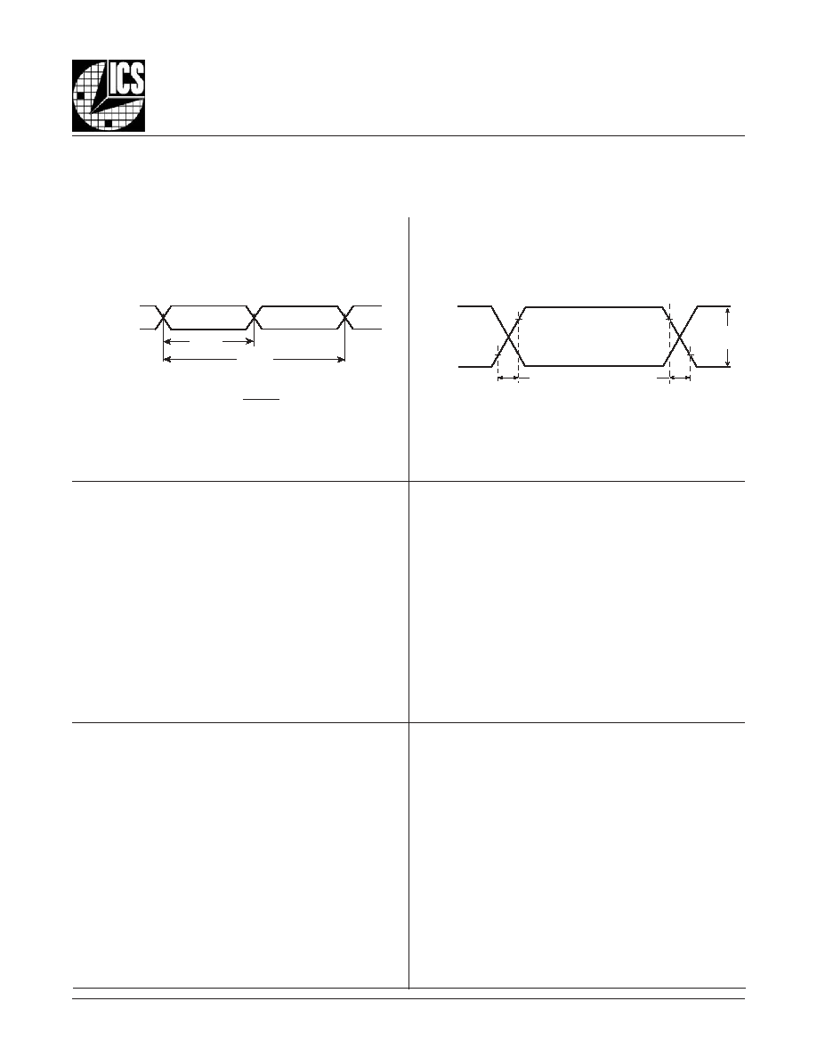
843034AY-01
www.icst.com/products/hiperclocks.html
REV. C NOVEMBER 28, 2005
13
Integrated
Circuit
Systems, Inc.
ICS843034-01
F
EMTO
C
LOCKS
TM
M
ULTI
-R
ATE
LVPECL F
REQUENCY
S
YNTHESIZER
PRELIMINARY
O
UTPUT
D
UTY
C
YCLE
/O
UTPUT
P
ULSE
W
IDTH
/P
ERIOD
O
UTPUT
R
ISE
/F
ALL
T
IME
Clock
Outputs
20%
80%
80%
20%
t
R
t
F
V
SW I N G
t
PW
t
PERIOD
t
PW
t
PERIOD
odc =
x 100%
FOUTA0
nFOUTA0
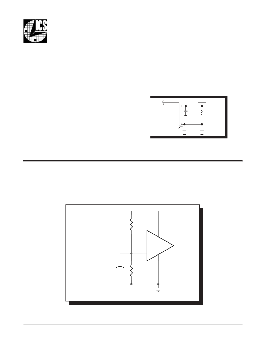
843034AY-01
www.icst.com/products/hiperclocks.html
REV. C NOVEMBER 28, 2005
14
Integrated
Circuit
Systems, Inc.
ICS843034-01
F
EMTO
C
LOCKS
TM
M
ULTI
-R
ATE
LVPECL F
REQUENCY
S
YNTHESIZER
PRELIMINARY
As in any high speed analog circuitry, the power supply pins
are vulnerable to random noise. The ICS843034-01 provides
separate power supplies to isolate any high switching
noise from the outputs to the internal PLL. V
CC
, V
CCA
, and V
CCO_x
should be individually connected to the power supply
plane through vias, and bypass capacitors should be
used for each pin. To achieve optimum jitter performance,
power supply isolation is required.
Figure 2
illustrates how
a 24
resistor along with a 10F and a .01F bypass
capacitor should be connected to each V
CCA
pin.
P
OWER
S
UPPLY
F
ILTERING
T
ECHNIQUES
F
IGURE
2. P
OWER
S
UPPLY
F
ILTERING
24
V
CCA
10
F
.01
F
3.3V
.01
F
V
CC
A
PPLICATION
I
NFORMATION
Figure 3
shows how the differential input can be wired to accept
single ended levels. The reference voltage V_REF = V
CC
/2 is
generated by the bias resistors R1, R2 and C1. This bias circuit
should be located as close as possible to the input pin. The ratio
W
IRING
THE
D
IFFERENTIAL
I
NPUT
TO
A
CCEPT
S
INGLE
E
NDED
LVCMOS/LVTTL L
EVELS
of R1 and R2 might need to be adjusted to position the V_REF in
the center of the input voltage swing. For example, if the input
clock swing is only 2.5V and V
CC
= 3.3V, V_REF should be 1.25V
and R2/R1 = 0.609.
V_REF
R1
1K
C1
0.1u
R2
1K
Single Ended Clock Input
CLK
nCLK
VCC
F
IGURE
3. S
INGLE
E
NDED
S
IGNAL
D
RIVING
D
IFFERENTIAL
I
NPUT
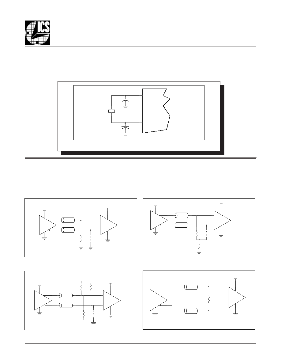
843034AY-01
www.icst.com/products/hiperclocks.html
REV. C NOVEMBER 28, 2005
15
Integrated
Circuit
Systems, Inc.
ICS843034-01
F
EMTO
C
LOCKS
TM
M
ULTI
-R
ATE
LVPECL F
REQUENCY
S
YNTHESIZER
PRELIMINARY
Figure 4. C
RYSTAL
I
NPU
t I
NTERFACE
ICS84332
C
RYSTAL
I
NPUT
I
NTERFACE
The ICS843034-01 has been characterized with 18pF paral-
lel resonant crystals. The capacitor values, C1 and C2, shown
in
Figure 4
below were determined using a 25MHz, 18pF
parallel resonant crystal and were chosen to minimize the
ppm error. The optimum C1 and C2 values can be slightly
adjusted for different board layouts.
ICS843034-01
C1
22p
X1
18pF Parallel Crystal
C2
22p
XTAL_OUT
XTAL_IN
F
IGURE
5C. H
I
P
ER
C
LOCK
S CLK/nCLK I
NPUT
D
RIVEN
BY
3.3V LVPECL D
RIVER
F
IGURE
5B. H
I
P
ER
C
LOCK
S CLK/nCLK I
NPUT
D
RIVEN
BY
3.3V LVPECL D
RIVER
F
IGURE
5D. H
I
P
ER
C
LOCK
S CLK/nCLK I
NPUT
D
RIVEN
BY
3.3V LVDS D
RIVER
3.3V
R1
50
R3
50
Zo = 50 Ohm
LVPECL
Zo = 50 Ohm
HiPerClockS
CLK
nCLK
3.3V
Input
R2
50
Zo = 50 Ohm
Input
HiPerClockS
CLK
nCLK
3.3V
R3
125
R2
84
Zo = 50 Ohm
3.3V
R4
125
LVPECL
R1
84
3.3V
D
IFFERENTIAL
C
LOCK
I
NPUT
I
NTERFACE
The CLK /nCLK accepts LVDS, LVPECL, LVHSTL, SSTL, HCSL
and other differential signals. Both V
SWING
and V
OH
must meet the
V
PP
and V
CMR
input requirements. Figures 5A to 5D show inter-
face examples for the HiPerClockS CLK/nCLK input driven by
the most common driver types. The input interfaces suggested
F
IGURE
5A. H
I
P
ER
C
LOCK
S CLK/nCLK I
NPUT
D
RIVEN
BY
ICS H
I
P
ER
C
LOCK
S LVHSTL D
RIVER
here are examples only. Please consult with the vendor of the
driver component to confirm the driver termination requirements.
For example in
Figure 5A,
the input termination applies for ICS
HiPerClockS LVHSTL drivers. If you are using an LVHSTL driver
from another vendor, use their termination recommendation.
1.8V
R2
50
Input
LVHSTL Driver
ICS
HiPerClockS
R1
50
LVHSTL
3.3V
Zo = 50 Ohm
Zo = 50 Ohm
HiPerClockS
CLK
nCLK
Zo = 50 Ohm
R1
100
3.3V
LVDS_Driv er
Zo = 50 Ohm
Receiv er
CLK
nCLK
3.3V
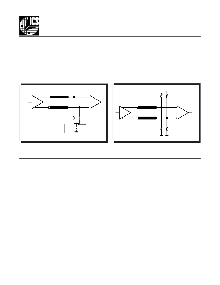
843034AY-01
www.icst.com/products/hiperclocks.html
REV. C NOVEMBER 28, 2005
16
Integrated
Circuit
Systems, Inc.
ICS843034-01
F
EMTO
C
LOCKS
TM
M
ULTI
-R
ATE
LVPECL F
REQUENCY
S
YNTHESIZER
PRELIMINARY
V
CC
- 2V
50
50
RTT
Z
o
= 50
Z
o
= 50
FOUT
FIN
RTT =
Z
o
1
((V
OH
+ V
OL
) / (V
CC
� 2)) � 2
3.3V
125
125
84
84
Z
o
= 50
Z
o
= 50
FOUT
FIN
The clock layout topology shown below is a typical termina-
tion for LVPECL outputs. The two different layouts mentioned
are recommended only as guidelines.
FOUTx and nFOUTx are low impedance follower outputs that
generate ECL/LVPECL compatible outputs. Therefore, terminat-
ing resistors (DC current path to ground) or current sources
must be used for functionality. These outputs are designed to
F
IGURE
6B. LVPECL O
UTPUT
T
ERMINATION
F
IGURE
6A. LVPECL O
UTPUT
T
ERMINATION
drive 50
transmission lines. Matched impedance techniques
should be used to maximize operating frequency and minimize
signal distortion.
Figures 6A and 6B
show two different layouts
which are recommended only as guidelines. Other suitable clock
layouts may exist and it would be recommended that the board
designers simulate to guarantee compatibility across all printed
circuit and clock component process variations.
T
ERMINATION
FOR
3.3V LVPECL O
UTPUT
I
NPUTS
:
C
RYSTAL
I
NPUT
:
For applications not requiring the use of the crystal oscillator
input, both XTAL_IN and XTAL_OUT can be left floating.
Though not required, but for additional protection, a 1k
resistor can be tied from XTAL_IN to ground.
CLK I
NPUT
:
For applications not requiring the use of a clock input, it can
be left floating. Though not required, but for additional
protection, a 1k
resistor can be tied from the CLK input to
ground.
CLK/nCLK I
NPUT
:
For applications not requiring the use of the differential input,
both CLK and nCLK can be left floating. Though not required,
but for additional protection, a 1k
resistor can be tied from
CLK to ground.
LVCMOS C
ONTROL
P
INS
:
All control pins have internal pull-ups or pull-downs; additional
resistance is not required but can be added for additional
protection. A 1k
resistor can be used.
R
ECOMMENDATIONS
FOR
U
NUSED
I
NPUT
AND
O
UTPUT
P
INS
O
UTPUTS
:
LVCMOS O
UTPUT
:
All unused LVCMOS output can be left floating. We
recommend that there is no trace attached.
LVPECL O
UTPUT
All unused LVPECL outputs can be left floating. We
recommend that there is no trace attached. Both sides of the
differential output pair should either be left floating or
terminated.

843034AY-01
www.icst.com/products/hiperclocks.html
REV. C NOVEMBER 28, 2005
17
Integrated
Circuit
Systems, Inc.
ICS843034-01
F
EMTO
C
LOCKS
TM
M
ULTI
-R
ATE
LVPECL F
REQUENCY
S
YNTHESIZER
PRELIMINARY
T
ERMINATION
FOR
2.5V LVPECL O
UTPUT
Figure 7A
and
Figure 7B
show examples of termination for
2.5V LVPECL driver. These terminations are equivalent to ter-
minating 50
to V
CC
- 2V. For V
CC
= 2.5V, the V
CC
- 2V is very
close to ground level. The R3 in
Figure 7B
can be eliminated
and the termination is shown in
Figure 7C.
F
IGURE
7C. 2.5V LVPECL T
ERMINATION
E
XAMPLE
R2
50
Zo = 50 Ohm
VCCO=2.5V
R1
50
Zo = 50 Ohm
+
-
2.5V
2,5V LVPECL
Driv er
F
IGURE
7B. 2.5V LVPECL D
RIVER
T
ERMINATION
E
XAMPLE
VCCO=2.5V
R1
50
R2
50
Zo = 50 Ohm
R3
18
2,5V LVPECL
Driv er
Zo = 50 Ohm
+
-
2.5V
F
IGURE
7A. 2.5V LVPECL D
RIVER
T
ERMINATION
E
XAMPLE
R2
62.5
2.5V
2,5V LVPECL
Driv er
R3
250
Zo = 50 Ohm
Zo = 50 Ohm
R4
62.5
2.5V
+
-
R1
250
VCCO=2.5V

843034AY-01
www.icst.com/products/hiperclocks.html
REV. C NOVEMBER 28, 2005
18
Integrated
Circuit
Systems, Inc.
ICS843034-01
F
EMTO
C
LOCKS
TM
M
ULTI
-R
ATE
LVPECL F
REQUENCY
S
YNTHESIZER
PRELIMINARY
P
OWER
C
ONSIDERATIONS
This section provides information on power dissipation and junction temperature for the ICS843034-01.
Equations and example calculations are also provided.
1. Power Dissipation.
The total power dissipation for the ICS843034-01 is the sum of the core power plus the power dissipated in the load(s).
The following is the power dissipation for V
CC
= 3.3V + 5% = 3.465V, which gives worst case results.
NOTE: Please refer to Section 3 for details on calculating power dissipated in the load.
�
Power (core)
MAX
= V
CC_MAX
* I
EE_MAX
= 3.465V * 185mA = 641mW
�
Power (outputs)
MAX
= 30mW/Loaded Output pair
If all outputs are loaded, the total power is 2 * 30mW = 60mW
Total Power
_MAX
(3.465V, with all outputs switching) = 641mW + 60mW = 701mW
2. Junction Temperature.
Junction temperature, Tj, is the temperature at the junction of the bond wire and bond pad and directly affects the reliability of the
device. The maximum recommended junction temperature for HiPerClockS
TM
devices is 125�C.
The equation for Tj is as follows: Tj =
JA
* Pd_total + T
A
Tj = Junction Temperature
JA
= Junction-to-Ambient Thermal Resistance
Pd_total = Total Device Power Dissipation (example calculation is in section 1 above)
T
A
= Ambient Temperature
In order to calculate junction temperature, the appropriate junction-to-ambient thermal resistance
JA
must be used. Assuming a
moderate air flow of 200 linear feet per minute and a multi-layer board, the appropriate value is 42.1�C/W per Table 8 below.
Therefore, Tj for an ambient temperature of 70�C with all outputs switching is:
70�C + 0.701W * 42.1�C/W = 99.5�C. This is well below the limit of 125�C.
This calculation is only an example. Tj will obviously vary depending on the number of loaded outputs, supply voltage, air flow,
and the type of board (single layer or multi-layer).
JA
by Velocity (Linear Feet per Minute)
T
ABLE
8. T
HERMAL
R
ESISTANCE
JA
FOR
48-
PIN
LQFP, F
ORCED
C
ONVECTION
0
200
500
Single-Layer PCB, JEDEC Standard Test Boards
67.8�C/W
55.9�C/W
50.1�C/W
Multi-Layer PCB, JEDEC Standard Test Boards
47.9�C/W
42.1�C/W
39.4�C/W
NOTE: Most modern PCB designs use multi-layered boards. The data in the second row pertains to most designs.
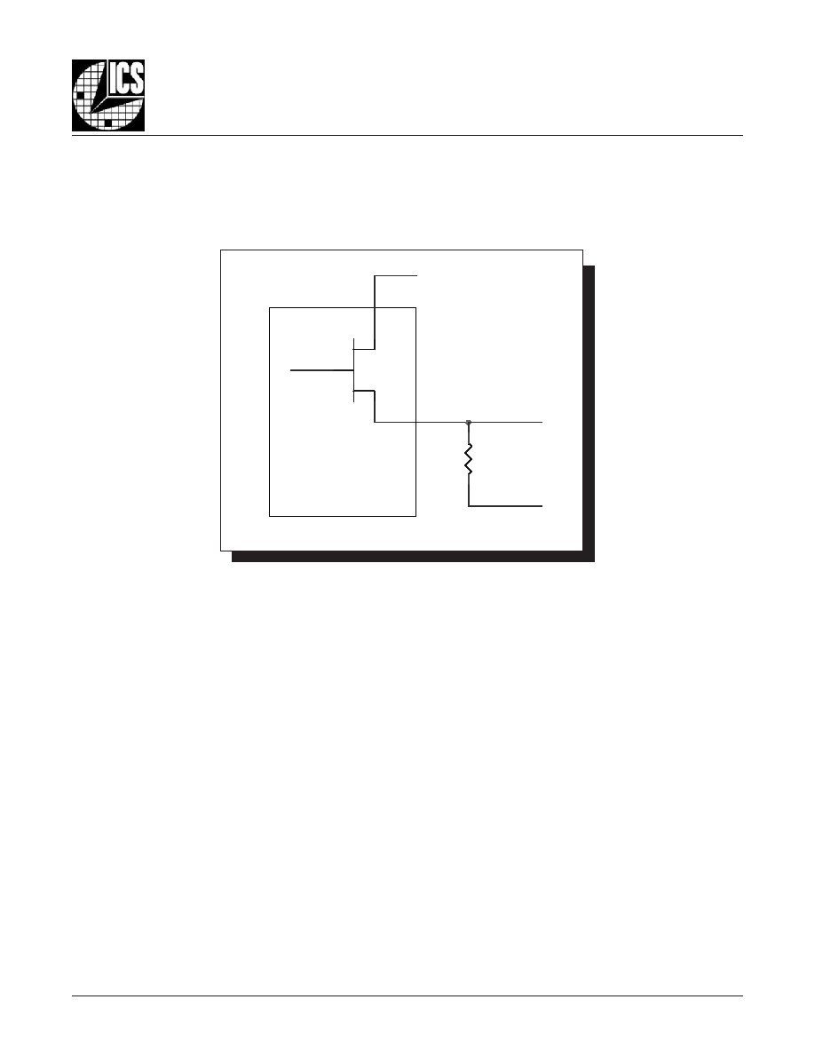
843034AY-01
www.icst.com/products/hiperclocks.html
REV. C NOVEMBER 28, 2005
19
Integrated
Circuit
Systems, Inc.
ICS843034-01
F
EMTO
C
LOCKS
TM
M
ULTI
-R
ATE
LVPECL F
REQUENCY
S
YNTHESIZER
PRELIMINARY
3. Calculations and Equations.
The purpose of this section is to derive the power dissipated into the load.
LVPECL output driver circuit and termination are shown in
Figure 8.
T
o calculate worst case power dissipation into the load, use the following equations which assume a 50
load, and a termination
voltage of V
CCO
- 2V.
�
For logic high, V
OUT
= V
OH_MAX
= V
CCO_MAX
� 0.9V
(V
CCO_MAX
- V
OH_MAX
) = 0.9V
�
For logic low, V
OUT
= V
OL_MAX
= V
CCO_MAX
� 1.7V
(V
CCO_MAX
- V
OL_MAX
) = 1.7V
Pd_H is power dissipation when the output drives high.
Pd_L is the power dissipation when the output drives low.
Pd_H = [(V
OH_MAX
� (V
CCO_MAX
- 2V))/R
L
] * (V
CCO_MAX
- V
OH_MAX
) = [(2V - (V
CCO_MAX
- V
OH_MAX
))/R
L
] * (V
CCO_MAX
- V
OH_MAX
) =
[(2V - 0.9V)/50
] * 0.9V = 19.8mW
Pd_L = [(V
OL_MAX
� (V
CCO_MAX
- 2V))/R
L
] * (V
CCO_MAX
- V
OL_MAX
) = [(2V - (V
CCO_MAX
- V
OL_MAX
))/R
L
] * (V
CCO_MAX
- V
OL_MAX
) =
[(2V - 1.7V)/50
] * 1.7V = 10.2mW
Total Power Dissipation per output pair = Pd_H + Pd_L = 30mW
F
IGURE
8. LVPECL D
RIVER
C
IRCUIT
AND
T
ERMINATION
Q1
V
OUT
V
CCO
R L
50
V
CCO
- 2V

843034AY-01
www.icst.com/products/hiperclocks.html
REV. C NOVEMBER 28, 2005
20
Integrated
Circuit
Systems, Inc.
ICS843034-01
F
EMTO
C
LOCKS
TM
M
ULTI
-R
ATE
LVPECL F
REQUENCY
S
YNTHESIZER
PRELIMINARY
R
ELIABILITY
I
NFORMATION
T
RANSISTOR
C
OUNT
The transistor count for ICS843034-01 is: 5084
T
ABLE
9.
JA
VS
. A
IR
F
LOW
T
ABLE
FOR
48 L
EAD
LQFP
JA
by Velocity (Linear Feet per Minute)
0
200
500
Single-Layer PCB, JEDEC Standard Test Boards
67.8�C/W
55.9�C/W
50.1�C/W
Multi-Layer PCB, JEDEC Standard Test Boards
47.9�C/W
42.1�C/W
39.4�C/W
NOTE: Most modern PCB designs use multi-layered boards. The data in the second row pertains to most designs.
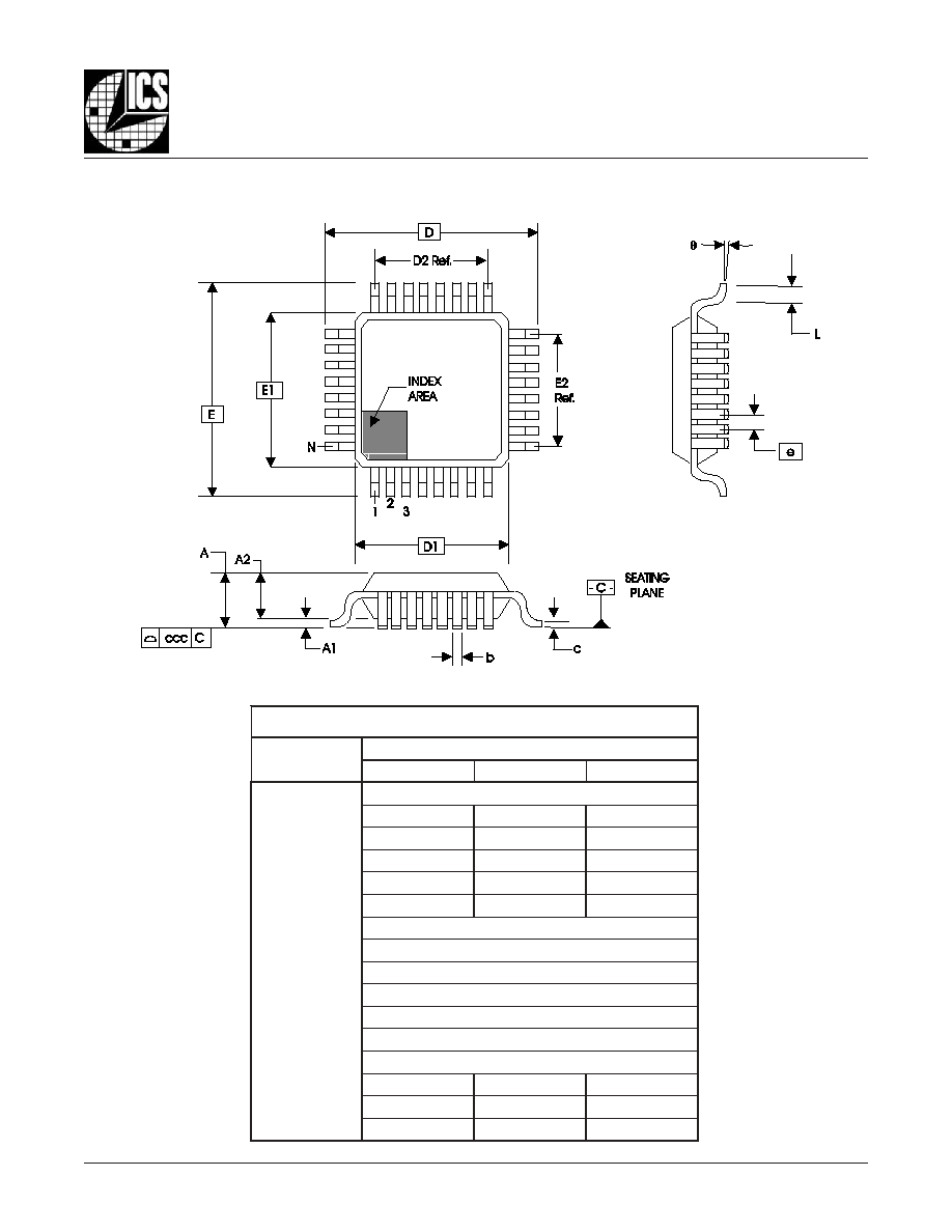
843034AY-01
www.icst.com/products/hiperclocks.html
REV. C NOVEMBER 28, 2005
21
Integrated
Circuit
Systems, Inc.
ICS843034-01
F
EMTO
C
LOCKS
TM
M
ULTI
-R
ATE
LVPECL F
REQUENCY
S
YNTHESIZER
PRELIMINARY
P
ACKAGE
O
UTLINE
- Y S
UFFIX
FOR
48 L
EAD
LQFP
T
ABLE
10. P
ACKAGE
D
IMENSIONS
Reference Document: JEDEC Publication 95, MS-026
N
O
I
T
A
I
R
A
V
C
E
D
E
J
S
R
E
T
E
M
I
L
L
I
M
N
I
S
N
O
I
S
N
E
M
I
D
L
L
A
L
O
B
M
Y
S
C
B
B
M
U
M
I
N
I
M
L
A
N
I
M
O
N
M
U
M
I
X
A
M
N
8
4
A
-
-
-
-
0
6
.
1
1
A
5
0
.
0
-
-
5
1
.
0
2
A
5
3
.
1
0
4
.
1
5
4
.
1
b
7
1
.
0
2
2
.
0
7
2
.
0
c
9
0
.
0
-
-
0
2
.
0
D
C
I
S
A
B
0
0
.
9
1
D
C
I
S
A
B
0
0
.
7
2
D
.
f
e
R
0
5
.
5
E
C
I
S
A
B
0
0
.
9
1
E
C
I
S
A
B
0
0
.
7
2
E
.
f
e
R
0
5
.
5
e
C
I
S
A
B
0
5
.
0
L
5
4
.
0
0
6
.
0
5
7
.
0
0
�
-
-
7
�
c
c
c
-
-
-
-
8
0
.
0

843034AY-01
www.icst.com/products/hiperclocks.html
REV. C NOVEMBER 28, 2005
22
Integrated
Circuit
Systems, Inc.
ICS843034-01
F
EMTO
C
LOCKS
TM
M
ULTI
-R
ATE
LVPECL F
REQUENCY
S
YNTHESIZER
PRELIMINARY
T
ABLE
11. O
RDERING
I
NFORMATION
While the information presented herein has been checked for both accuracy and reliability, Integrated Circuit Systems, Incorporated (ICS) assumes no responsibility for either its use
or for infringement of any patents or other rights of third parties, which would result from its use. No other circuits, patents, or licenses are implied. This product is intended for use
in normal commercial applications. Any other applications such as those requiring extended temperature range, high reliability, or other extraordinary environmental requirements are
not recommended without additional processing by ICS. ICS reserves the right to change any circuitry or specifications without notice. ICS does not authorize or warrant any ICS
product for use in life support devices or critical medical instruments.
The aforementioned trademark, HiPerClockSTM and F
EMTO
C
LOCKS
TM is a trademark of Integrated Circuit Systems, Inc. or its subsidiaries in the United States and/or other countries.
r
e
b
m
u
N
r
e
d
r
O
/
t
r
a
P
g
n
i
k
r
a
M
e
g
a
k
c
a
P
g
n
i
g
a
k
c
a
P
g
n
i
p
p
i
h
S
e
r
u
t
a
r
e
p
m
e
T
1
0
-
Y
A
4
3
0
3
4
8
S
C
I
1
0
A
4
3
0
3
4
8
S
C
I
P
F
Q
L
d
a
e
L
8
4
y
a
r
t
C
�
0
7
o
t
C
�
0
T
1
0
-
Y
A
4
3
0
3
4
8
S
C
I
1
0
A
4
3
0
3
4
8
S
C
I
P
F
Q
L
d
a
e
L
8
4
l
e
e
r
&
e
p
a
t
0
0
0
1
C
�
0
7
o
t
C
�
0
F
L
1
0
-
Y
A
4
3
0
3
4
8
S
C
I
L
1
0
A
4
3
0
3
4
S
C
I
P
F
Q
L
"
e
e
r
F
-
d
a
e
L
"
d
a
e
L
8
4
y
a
r
t
C
�
0
7
o
t
C
�
0
T
F
L
1
0
-
Y
A
4
3
0
3
4
8
S
C
I
L
1
0
A
4
3
0
3
4
S
C
I
P
F
Q
L
"
e
e
r
F
-
d
a
e
L
"
d
a
e
L
8
4
l
e
e
r
&
e
p
a
t
0
0
0
1
C
�
0
7
o
t
C
�
0
.
t
n
a
il
p
m
o
c
S
H
o
R
e
r
a
d
n
a
n
o
i
t
a
r
u
g
i
f
n
o
c
e
e
r
F
-
b
P
e
h
t
e
r
a
r
e
b
m
u
n
t
r
a
p
e
h
t
o
t
x
i
f
f
u
s
"
F
L
"
n
a
h
t
i
w
d
e
r
d
r
o
e
r
a
t
a
h
t
s
t
r
a
P
:
E
T
O
N