Document Outline
- General Description
- Features
- Common Configuration Table
- Block Diagram
- Pin Assignment
- Pin Descriptions
- Pin Characteristics
- Absolute Maximum Ratings
- 3.3V Power Supply DC Characteristics
- 2.5V Power Supply DC Characteristics
- LVCMOS DC Characteristics
- LVPECL DC Characteristics
- Crystal Characteristics
- 3.3V AC Characteristics
- 2.5V AC Characteristics
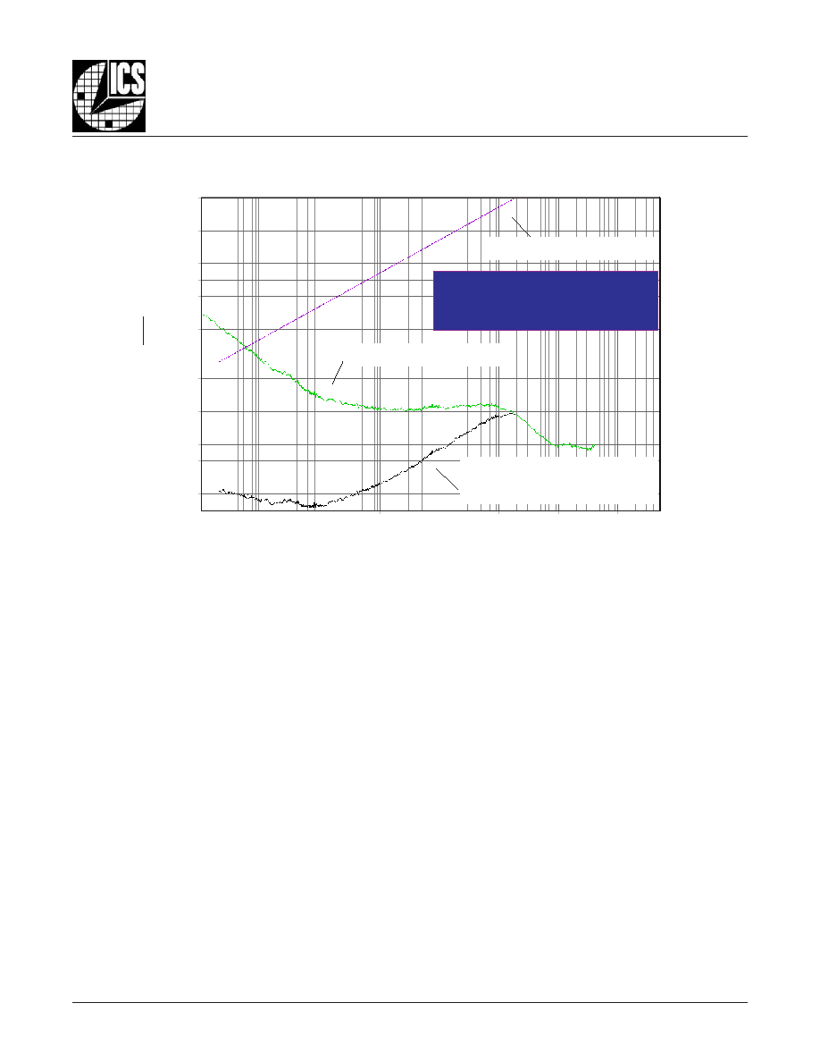
- Typical Phase Noise Plot @ 75MHz
- Typical Phase Noise Plot @ 150MHz
- Typical Phase Noise Plot @ 159.375MHz
- Parameter Measurement Information
- Application Information
- Power Supply Filtering Techniques
- Crystal Input Interface
- Termination for 3.3V LVPECL Output
- Termination for 2.5V LVPECL Output
- Power Considerations
- Power Dissipation
- Junction Temperature
- Thermal Resistance
- Calculations & Equations
- LVPECL Driver Circuit & Termination Diagram
- Reliability Information
- Transistor Count
- Package Outline
- Package Dimensions
- Ordering Information

843071AGI
www.icst.com/products/hiperclocks.html
REV. A JANUARY 11, 2006
1
Integrated
Circuit
Systems, Inc.
ICS843071I
F
EMTO
C
LOCKS
TM C
RYSTAL
-
TO
- LVPECL
C
LOCK
G
ENERATOR
G
ENERAL
D
ESCRIPTION
The ICS843071I is a Serial ATA (SATA)/Serial
Attached SCSI (SAS) Clock Generator and a
member of the HiPerClocks
TM
family of high
performance devices from ICS. The ICS843071I
uses an 18pF parallel resonant crystal over
the range of 20.833MHz - 28.3MHz. For SATA/SAS
applications, a 25MHz crystal is used and either 75MHz or
150MHz may be selected with the FREQ_SEL pin. For 10Gb
Fibre Channel applications, a 26.5625MHz crystal is used
for 159.375MHz output. The ICS843071I has excellent
<1ps phase jitter performance, over the 12kHz - 20MHz
integration range. The ICS843071I is packaged in a small
8-pin TSSOP, making it ideal for use in systems with limited
board space.
F
EATURES
� One Differential LVPECL output
� Crystal oscillator interface, 18pF parallel resonant crystal
(20.833MHz - 28.3MHz)
� Output frequency range: 62.5MHz - 170MHz
� VCO range: 500MHz - 680MHz
� RMS phase jitter @ 150MHz, using a 25MHz crystal
(12kHz - 20MHz): 0.64ps (typical) @ 3.3V output
� RMS phase jitter @ 159.375MHz, using a 26.5625MHz
crystal (1.875MHz - 20MHz): 0.40ps (typical) @ 3.3V
output
� 3.3V or 2.5V operating supply
� -40�C to 85�C ambient operating temperature
� Available in both standard and lead-free RoHS compliant
packages
HiPerClockSTM
ICS
ICS843071I
8-Lead TSSOP
4.40mm x 3.0mm x 0.925mm
package body
G Package
Top View
V
CCA
XTAL_OUT
XTAL_IN
V
EE
1
2
3
4
V
CC
Q
nQ
FREQ_SEL
8
7
6
5
B
LOCK
D
IAGRAM
OSC
Phase
Detector
VCO
500MHz - 680MHz
M = �24
(fixed)
FREQ_SEL N
0 �4
1 �8
XTAL_IN
XTAL_OUT
Q
nQ
C
OMMON
C
ONFIGURATION
T
ABLE
- S
ERIAL
ATA/S
ERIAL
A
TTACHED
SCSI
P
IN
A
SSIGNMENT
FREQ_SEL
Pullup
s
t
u
p
n
I
y
c
n
e
u
q
e
r
F
t
u
p
t
u
O
)
z
H
M
(
)
z
H
M
(
y
c
n
e
u
q
e
r
F
l
a
t
s
y
r
C
L
E
S
_
Q
E
R
F
M
N
n
o
i
t
a
c
i
l
p
i
t
l
u
M
N
/
M
e
u
l
a
V
5
2
0
4
2
4
6
0
5
1
5
2
1
4
2
8
3
5
7
5
2
6
5
.
6
2
0
4
2
4
6
5
7
3
.
9
5
1
843071AGI
www.icst.com/products/hiperclocks.html
REV. A JANUARY 11, 2006
2
Integrated
Circuit
Systems, Inc.
ICS843071I
F
EMTO
C
LOCKS
TM C
RYSTAL
-
TO
- LVPECL
C
LOCK
G
ENERATOR
T
ABLE
2. P
IN
C
HARACTERISTICS
T
ABLE
1. P
IN
D
ESCRIPTIONS
l
o
b
m
y
S
r
e
t
e
m
a
r
a
P
s
n
o
i
t
i
d
n
o
C
t
s
e
T
m
u
m
i
n
i
M
l
a
c
i
p
y
T
m
u
m
i
x
a
M
s
t
i
n
U
C
N
I
e
c
n
a
t
i
c
a
p
a
C
t
u
p
n
I
4
F
p
R
P
U
L
L
U
P
r
o
t
s
i
s
e
R
p
u
ll
u
P
t
u
p
n
I
1
5
k
r
e
b
m
u
N
e
m
a
N
e
p
y
T
n
o
i
t
p
i
r
c
s
e
D
1
V
A
C
C
r
e
w
o
P
.
n
i
p
y
l
p
p
u
s
g
o
l
a
n
A
3
,
2
,
T
U
O
_
L
A
T
X
N
I
_
L
A
T
X
t
u
p
n
I
,
t
u
p
n
i
e
h
t
s
i
N
I
_
L
A
T
X
.
e
c
a
f
r
e
t
n
i
r
o
t
a
ll
i
c
s
o
l
a
t
s
y
r
C
.
t
u
p
t
u
o
e
h
t
s
i
T
U
O
_
L
A
T
X
4
V
E
E
r
e
w
o
P
.
n
i
p
y
l
p
p
u
s
e
v
i
t
a
g
e
N
5
L
E
S
_
Q
E
R
F
t
u
p
n
I
p
u
ll
u
P
.
s
l
e
v
e
l
e
c
a
f
r
e
t
n
i
L
T
T
V
L
/
S
O
M
C
V
L
.
n
i
p
t
c
e
l
e
s
y
c
n
e
u
q
e
r
F
7
,
6
Q
,
Q
n
t
u
p
t
u
O
.
s
l
e
v
e
l
e
c
a
f
r
e
t
n
i
L
C
E
P
V
L
.
s
t
u
p
t
u
o
k
c
o
l
c
l
a
i
t
n
e
r
e
f
f
i
D
8
V
C
C
r
e
w
o
P
.
n
i
p
y
l
p
p
u
s
e
r
o
C
:
E
T
O
N
p
u
ll
u
P
.
s
e
u
l
a
v
l
a
c
i
p
y
t
r
o
f
,
s
c
i
t
s
i
r
e
t
c
a
r
a
h
C
n
i
P
,
2
e
l
b
a
T
e
e
S
.
s
r
o
t
s
i
s
e
r
t
u
p
n
i
l
a
n
r
e
t
n
i
o
t
s
r
e
f
e
r
843071AGI
www.icst.com/products/hiperclocks.html
REV. A JANUARY 11, 2006
3
Integrated
Circuit
Systems, Inc.
ICS843071I
F
EMTO
C
LOCKS
TM C
RYSTAL
-
TO
- LVPECL
C
LOCK
G
ENERATOR
T
ABLE
3A. P
OWER
S
UPPLY
DC C
HARACTERISTICS
,
V
CC
= V
CCA
= 3.3V�10%, T
A
= -40�C
TO
85�C
A
BSOLUTE
M
AXIMUM
R
ATINGS
Supply Voltage, V
DD
4.6V
Inputs, V
I
-0.5V to V
CC
+ 0.5 V
Outputs, I
O
(LVDS)
Continuous Current
10mA
Surge Current
15mA
Package Thermal Impedance,
JA
101.7�C/W (0 mps)
Storage Temperature, T
STG
-65�C to 150�C
NOTE: Stresses beyond those listed under Absolute
Maximum Ratings may cause permanent damage to the
device. These ratings are stress specifications only. Functional
operation of product at these conditions or any conditions be-
yond those listed in the
DC Characteristics
or
AC Character-
istics
is not implied. Exposure to absolute maximum rating
conditions for extended periods may affect product reliability.
T
ABLE
3C. LVCMOS/LVTTL DC C
HARACTERISTICS
,
V
CC
= V
CCA
= 3.3V�10%
OR
2.5V�10%, T
A
= -40�C
TO
85�C
T
ABLE
3B. P
OWER
S
UPPLY
DC C
HARACTERISTICS
,
V
CC
= V
CCA
= 2.5V�10%, T
A
= -40�C
TO
85�C
l
o
b
m
y
S
r
e
t
e
m
a
r
a
P
s
n
o
i
t
i
d
n
o
C
t
s
e
T
m
u
m
i
n
i
M
l
a
c
i
p
y
T
m
u
m
i
x
a
M
s
t
i
n
U
V
H
I
e
g
a
t
l
o
V
h
g
i
H
t
u
p
n
I
V
3
.
3
2
V
C
C
3
.
0
+
V
V
5
.
2
7
.
1
V
C
C
3
.
0
+
V
V
L
I
e
g
a
t
l
o
V
w
o
L
t
u
p
n
I
V
3
.
3
3
.
0
-
8
.
0
V
V
5
.
2
3
.
0
-
7
.
0
V
I
H
I
t
n
e
r
r
u
C
h
g
i
H
t
u
p
n
I
V
C
C
V
=
N
I
V
5
7
.
2
r
o
V
3
6
.
3
=
5
A
�
I
L
I
t
n
e
r
r
u
C
w
o
L
t
u
p
n
I
V
C
C
V
,
V
5
7
.
2
r
o
V
3
6
.
3
=
N
I
V
0
=
0
5
1
-
A
�
l
o
b
m
y
S
r
e
t
e
m
a
r
a
P
s
n
o
i
t
i
d
n
o
C
t
s
e
T
m
u
m
i
n
i
M
l
a
c
i
p
y
T
m
u
m
i
x
a
M
s
t
i
n
U
V
C
C
e
g
a
t
l
o
V
y
l
p
p
u
S
e
v
i
t
i
s
o
P
0
.
3
3
.
3
3
6
.
3
V
V
A
C
C
e
g
a
t
l
o
V
y
l
p
p
u
S
g
o
l
a
n
A
0
.
3
3
.
3
3
6
.
3
V
I
C
C
t
n
e
r
r
u
C
y
l
p
p
u
S
r
e
w
o
P
6
9
A
m
I
A
C
C
t
n
e
r
r
u
C
y
l
p
p
u
S
g
o
l
a
n
A
2
1
A
m
I
E
E
t
n
e
r
r
u
C
y
l
p
p
u
S
r
e
w
o
P
2
7
A
m
l
o
b
m
y
S
r
e
t
e
m
a
r
a
P
s
n
o
i
t
i
d
n
o
C
t
s
e
T
m
u
m
i
n
i
M
l
a
c
i
p
y
T
m
u
m
i
x
a
M
s
t
i
n
U
V
C
C
e
g
a
t
l
o
V
y
l
p
p
u
S
e
v
i
t
i
s
o
P
5
2
.
2
5
.
2
5
7
.
2
V
V
A
C
C
e
g
a
t
l
o
V
y
l
p
p
u
S
g
o
l
a
n
A
5
2
.
2
5
.
2
5
7
.
2
V
I
C
C
t
n
e
r
r
u
C
y
l
p
p
u
S
r
e
w
o
P
2
7
A
m
I
A
C
C
t
n
e
r
r
u
C
y
l
p
p
u
S
g
o
l
a
n
A
2
1
A
m
I
E
E
t
n
e
r
r
u
C
y
l
p
p
u
S
r
e
w
o
P
2
7
A
m
843071AGI
www.icst.com/products/hiperclocks.html
REV. A JANUARY 11, 2006
4
Integrated
Circuit
Systems, Inc.
ICS843071I
F
EMTO
C
LOCKS
TM C
RYSTAL
-
TO
- LVPECL
C
LOCK
G
ENERATOR
T
ABLE
4. C
RYSTAL
C
HARACTERISTICS
T
ABLE
5A. AC C
HARACTERISTICS
,
V
CC
= V
CCA
= 3.3V�10%, T
A
= -40�C
TO
85�C
T
ABLE
5B. AC C
HARACTERISTICS
,
V
CC
= V
CCA
= 2.5V�10%, T
A
= -40�C
TO
85�C
T
ABLE
3D. LVPECL DC C
HARACTERISTICS
,
V
CC
= V
CCA
= 3.3V�10%
OR
2.5V�10%, T
A
= -40�C
TO
85�C
l
o
b
m
y
S
r
e
t
e
m
a
r
a
P
s
n
o
i
t
i
d
n
o
C
t
s
e
T
m
u
m
i
n
i
M
l
a
c
i
p
y
T
m
u
m
i
x
a
M
s
t
i
n
U
V
H
O
1
E
T
O
N
;
e
g
a
t
l
o
V
h
g
i
H
t
u
p
t
u
O
V
C
C
4
.
1
-
V
C
C
9
.
0
-
V
V
L
O
1
E
T
O
N
;
e
g
a
t
l
o
V
w
o
L
t
u
p
t
u
O
V
C
C
0
.
2
-
V
C
C
7
.
1
-
V
V
G
N
I
W
S
g
n
i
w
S
e
g
a
t
l
o
V
t
u
p
t
u
O
k
a
e
P
-
o
t
-
k
a
e
P
6
.
0
0
.
1
V
0
5
h
t
i
w
d
e
t
a
n
i
m
r
e
t
s
t
u
p
t
u
O
:
1
E
T
O
N
V
o
t
C
C
.
V
2
-
r
e
t
e
m
a
r
a
P
s
n
o
i
t
i
d
n
o
C
t
s
e
T
m
u
m
i
n
i
M
l
a
c
i
p
y
T
m
u
m
i
x
a
M
s
t
i
n
U
n
o
i
t
a
ll
i
c
s
O
f
o
e
d
o
M
l
a
t
n
e
m
a
d
n
u
F
y
c
n
e
u
q
e
r
F
3
3
8
.
0
2
3
.
8
2
z
H
M
)
R
S
E
(
e
c
n
a
t
s
i
s
e
R
s
e
i
r
e
S
t
n
e
l
a
v
i
u
q
E
0
5
e
c
n
a
t
i
c
a
p
a
C
t
n
u
h
S
7
F
p
l
e
v
e
L
e
v
i
r
D
1
W
m
l
o
b
m
y
S
r
e
t
e
m
a
r
a
P
s
n
o
i
t
i
d
n
o
C
t
s
e
T
m
u
m
i
n
i
M
l
a
c
i
p
y
T
m
u
m
i
x
a
M
s
t
i
n
U
f
T
U
O
y
c
n
e
u
q
e
r
F
t
u
p
t
u
O
5
.
2
6
0
7
1
z
H
M
t
)
�
(
t
ij
;
)
m
o
d
n
a
R
(
r
e
t
t
i
J
e
s
a
h
P
S
M
R
1
E
T
O
N
:
e
g
n
a
R
n
o
i
t
a
r
g
e
t
n
I
@
z
H
M
0
5
1
z
H
M
0
2
-
z
H
k
2
1
4
6
.
0
s
p
:
e
g
n
a
R
n
o
i
t
a
r
g
e
t
n
I
@
z
H
M
5
7
z
H
M
0
2
-
z
H
k
2
1
4
6
.
0
s
p
:
e
g
n
a
R
n
o
i
t
a
r
g
e
t
n
I
@
z
H
M
5
7
3
.
9
5
1
z
H
M
0
2
-
z
H
M
5
7
8
.
1
0
4
.
0
s
p
t
R
t
/
F
e
m
i
T
ll
a
F
/
e
s
i
R
t
u
p
t
u
O
%
0
8
o
t
%
0
2
0
5
2
0
0
5
s
p
c
d
o
e
l
c
y
C
y
t
u
D
t
u
p
t
u
O
8
4
2
5
%
.
n
o
i
t
c
e
s
s
i
h
t
g
n
i
w
o
ll
o
f
s
t
o
l
P
e
s
i
o
N
e
s
a
h
P
e
h
t
o
t
r
e
f
e
r
e
s
a
e
l
P
:
1
E
T
O
N
l
o
b
m
y
S
r
e
t
e
m
a
r
a
P
s
n
o
i
t
i
d
n
o
C
t
s
e
T
m
u
m
i
n
i
M
l
a
c
i
p
y
T
m
u
m
i
x
a
M
s
t
i
n
U
f
T
U
O
y
c
n
e
u
q
e
r
F
t
u
p
t
u
O
5
.
2
6
0
7
1
z
H
M
t
)
�
(
t
ij
)
m
o
d
n
a
R
(
r
e
t
t
i
J
e
s
a
h
P
S
M
R
:
e
g
n
a
R
n
o
i
t
a
r
g
e
t
n
I
@
z
H
M
0
5
1
z
H
M
0
2
-
z
H
k
2
1
4
9
.
0
s
p
:
e
g
n
a
R
n
o
i
t
a
r
g
e
t
n
I
@
z
H
M
5
7
z
H
M
0
2
-
z
H
k
2
1
0
8
.
0
s
p
:
e
g
n
a
R
n
o
i
t
a
r
g
e
t
n
I
@
z
H
M
5
7
3
.
9
5
1
z
H
M
0
2
-
z
H
M
5
7
8
.
1
2
4
.
0
s
p
t
R
t
/
F
e
m
i
T
ll
a
F
/
e
s
i
R
t
u
p
t
u
O
%
0
8
o
t
%
0
2
0
5
2
0
0
5
s
p
c
d
o
e
l
c
y
C
y
t
u
D
t
u
p
t
u
O
8
4
2
5
%
843071AGI
www.icst.com/products/hiperclocks.html
REV. A JANUARY 11, 2006
5
Integrated
Circuit
Systems, Inc.
ICS843071I
F
EMTO
C
LOCKS
TM C
RYSTAL
-
TO
- LVPECL
C
LOCK
G
ENERATOR
T
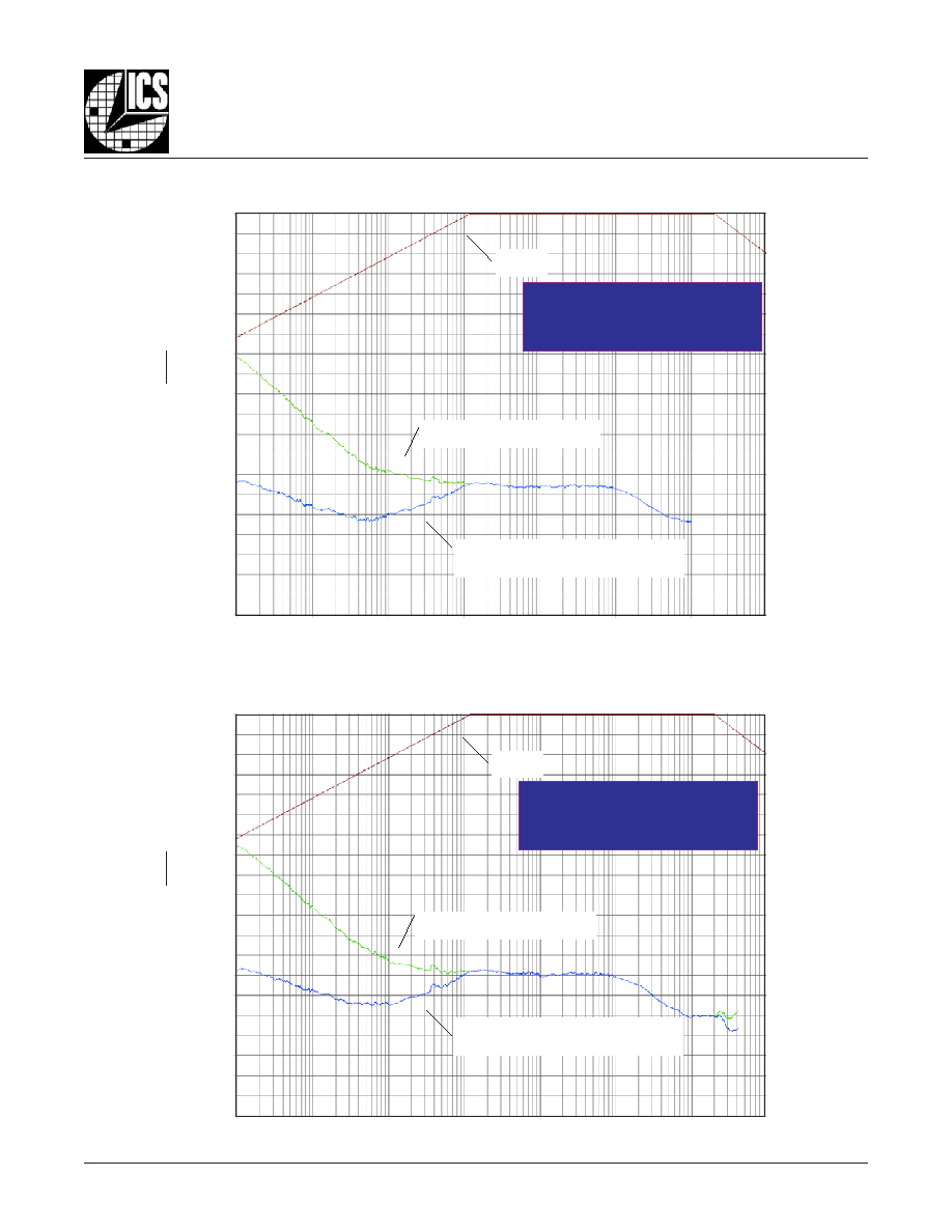
YPICAL
P
HASE
N
OISE
AT
75MH
Z
@ 3.3V
75MHz
RMS Phase Noise Jitter
12kHz to 20MHz = 0.64ps (typical)
O
FFSET
F
REQUENCY
(H
Z
)
dBc
Hz
N
OISE
P
O
WER
10
100
1k
10k
100k
1M
10M
100M
0
-10
-20
-30
-40
-50
-60
-70
-80
-90
-100
-110
-120
-130
-140
-150
-160
-170
-180
-190
-200
Phase Noise Result by adding
a Filter to raw data
Raw Phase Noise Data
Filter
T
YPICAL
P
HASE
N
OISE
AT
150MH
Z
@ 3.3V
150MHz
RMS Phase Noise Jitter
12kHz to 20MHz = 0.64ps (typical)
O
FFSET
F
REQUENCY
(H
Z
)
dBc
Hz
N
OISE
P
O
WER
10
100
1k
10k
100k
1M
10M
100M
0
-10
-20
-30
-40
-50
-60
-70
-80
-90
-100
-110
-120
-130
-140
-150
-160
-170
-180
-190
-200
Phase Noise Result by adding
a Filter to raw data
Raw Phase Noise Data
Filter
843071AGI
www.icst.com/products/hiperclocks.html
REV. A JANUARY 11, 2006
6
Integrated
Circuit
Systems, Inc.
ICS843071I
F
EMTO
C
LOCKS
TM C
RYSTAL
-
TO
- LVPECL
C
LOCK
G
ENERATOR
T
YPICAL
P
HASE
N
OISE
AT
159.375MH
Z
@ 3.3V
159.375MHz
RMS Phase Noise Jitter
1.875MHz to 20MHz = 0.40ps (typical)
O
FFSET
F
REQUENCY
(H
Z
)
dBc
Hz
N
OISE
P
O
WER
10
100
1k
10k
100k
1M
10M
100M
500M
0
-10
-20
-30
-40
-50
-60
-70
-80
-90
-100
-110
-120
-130
-140
-150
-160
-170
-180
-190
-200
Phase Noise Result by adding
a 10Gb Fibre Channel Filter to
raw data
Raw Phase Noise Data
10Gb Fibre Channel Filter

843071AGI
www.icst.com/products/hiperclocks.html
REV. A JANUARY 11, 2006
7
Integrated
Circuit
Systems, Inc.
ICS843071I
F
EMTO
C
LOCKS
TM C
RYSTAL
-
TO
- LVPECL
C
LOCK
G
ENERATOR
P
ARAMETER
M
EASUREMENT
I
NFORMATION
RMS P
HASE
J
ITTER
LVPECL 3.3V O
UTPUT
L
OAD
AC T
EST
C
IRCUIT
LVPECL 2.5V O
UTPUT
L
OAD
AC T
EST
C
IRCUIT
O
UTPUT
R
ISE
/F
ALL
T
IME
O
UTPUT
D
UTY
C
YCLE
/P
ULSE
W
IDTH
/P
ERIOD
Q
nQ
Clock
Outputs
20%
80%
80%
20%
t
R
t
F
V
SW I N G
SCOPE
Qx
nQx
LVPECL
2V
-1.3V � 0.330V
V
EE
V
CC,
V
CCA
SCOPE
Qx
nQx
LVPECL
2V
-0.5V � 0.250V
V
EE
V
CC,
V
CCA
t
PW
t
PERIOD
t
PW
t
PERIOD
odc =
x 100%
Phase Noise Mask
Offset Frequency
f
1
f
2
Phase Noise Plot
RMS Jitter = Area Under the Masked Phase Noise Plot
Noise P
o
w
er
843071AGI
www.icst.com/products/hiperclocks.html
REV. A JANUARY 11, 2006
8
Integrated
Circuit
Systems, Inc.
ICS843071I
F
EMTO
C
LOCKS
TM C
RYSTAL
-
TO
- LVPECL
C
LOCK
G
ENERATOR
A
PPLICATION
I
NFORMATION
P
OWER
S
UPPLY
F
ILTERING
T
ECHNIQUES
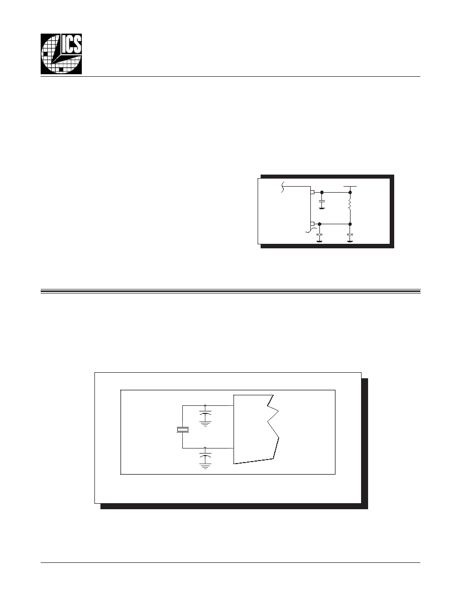
As in any high speed analog circuitry, the power supply pins
are vulnerable to random noise. The ICS843071I provides
separate power supplies to isolate any high switching
noise from the outputs to the internal PLL. V
CC
and V
CCA
should
b e i n d i v i d u a l l y c o n n e c t e d t o t h e p o w e r s u p p l y
plane through vias, and bypass capacitors should be
used for each pin. To achieve optimum jitter performance,
power supply isolation is required.
Figure 1
illustrates how
a 10
resistor along with a 10F and a .01F bypass
capacitor should be connected to each V
CCA
pin.
F
IGURE
1. P
OWER
S
UPPLY
F
ILTERING
10
V
CCA
10
F
.01
F
3.3V or 2.5V
.01
F
V
CC
Figure 2. C
RYSTAL
I
NPU
t I
NTERFACE
C
RYSTAL
I
NPUT
I
NTERFACE
The ICS843071I has been characterized with 18pF parallel
resonant crystals. The capacitor values, C1 and C2, shown in
Figure 2
below were determined using an 18pF parallel reso-
nant crystal and were chosen to minimize the ppm error. The
optimum C1 and C2 values can be slightly adjusted for differ-
ent board layouts.
ICS84332
XTAL_IN
XTAL_OUT
X1
18pF Parallel Cry stal
C2
22p
C1
22p
ICS843071I
843071AGI
www.icst.com/products/hiperclocks.html
REV. A JANUARY 11, 2006
9
Integrated
Circuit
Systems, Inc.
ICS843071I
F
EMTO
C
LOCKS
TM C
RYSTAL
-
TO
- LVPECL
C
LOCK
G
ENERATOR
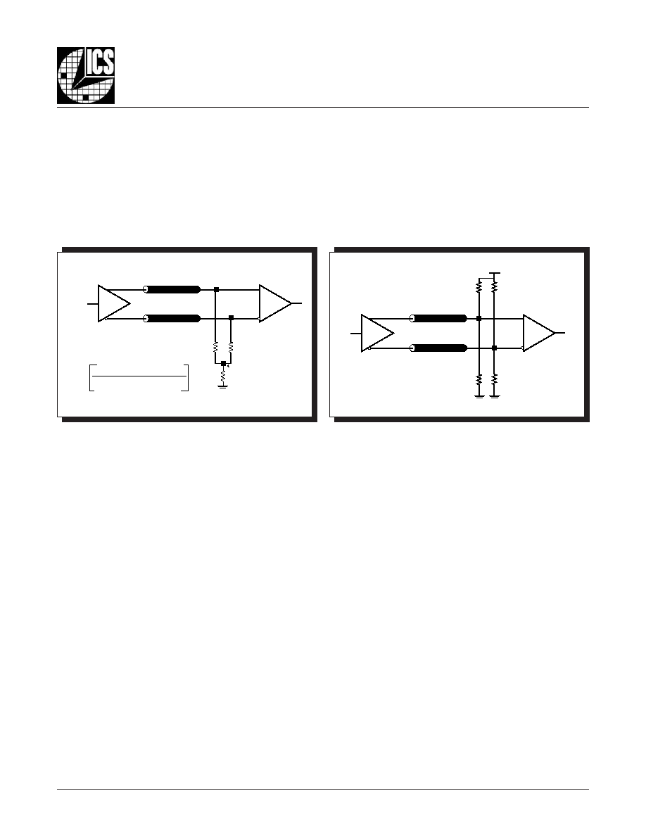
T
ERMINATION
FOR
3.3V LVPECL O
UTPUT
The clock layout topology shown below is a typical termina-
tion for LVPECL outputs. The two different layouts mentioned
are recommended only as guidelines.
FOUT and nFOUT are low impedance follower outputs that
generate ECL/LVPECL compatible outputs. Therefore, terminat-
ing resistors (DC current path to ground) or current sources
must be used for functionality. These outputs are designed to
F
IGURE
3B. LVPECL O
UTPUT
T
ERMINATION
F
IGURE
3A. LVPECL O
UTPUT
T
ERMINATION
drive 50
transmission lines. Matched impedance techniques
should be used to maximize operating frequency and minimize
signal distortion.
Figures 3A and 3B
show two different layouts
which are recommended only as guidelines. Other suitable clock
layouts may exist and it would be recommended that the board
designers simulate to guarantee compatibility across all printed
circuit and clock component process variations.
V
CC
- 2V
50
50
RTT
Z
o
= 50
Z
o
= 50
FOUT
FIN
RTT =
Z
o
1
((V
OH
+ V
OL
) / (V
CC
� 2)) � 2
3.3V
125
125
84
84
Z
o
= 50
Z
o
= 50
FOUT
FIN
843071AGI
www.icst.com/products/hiperclocks.html
REV. A JANUARY 11, 2006
10
Integrated
Circuit
Systems, Inc.
ICS843071I
F
EMTO
C
LOCKS
TM C
RYSTAL
-
TO
- LVPECL
C
LOCK
G
ENERATOR
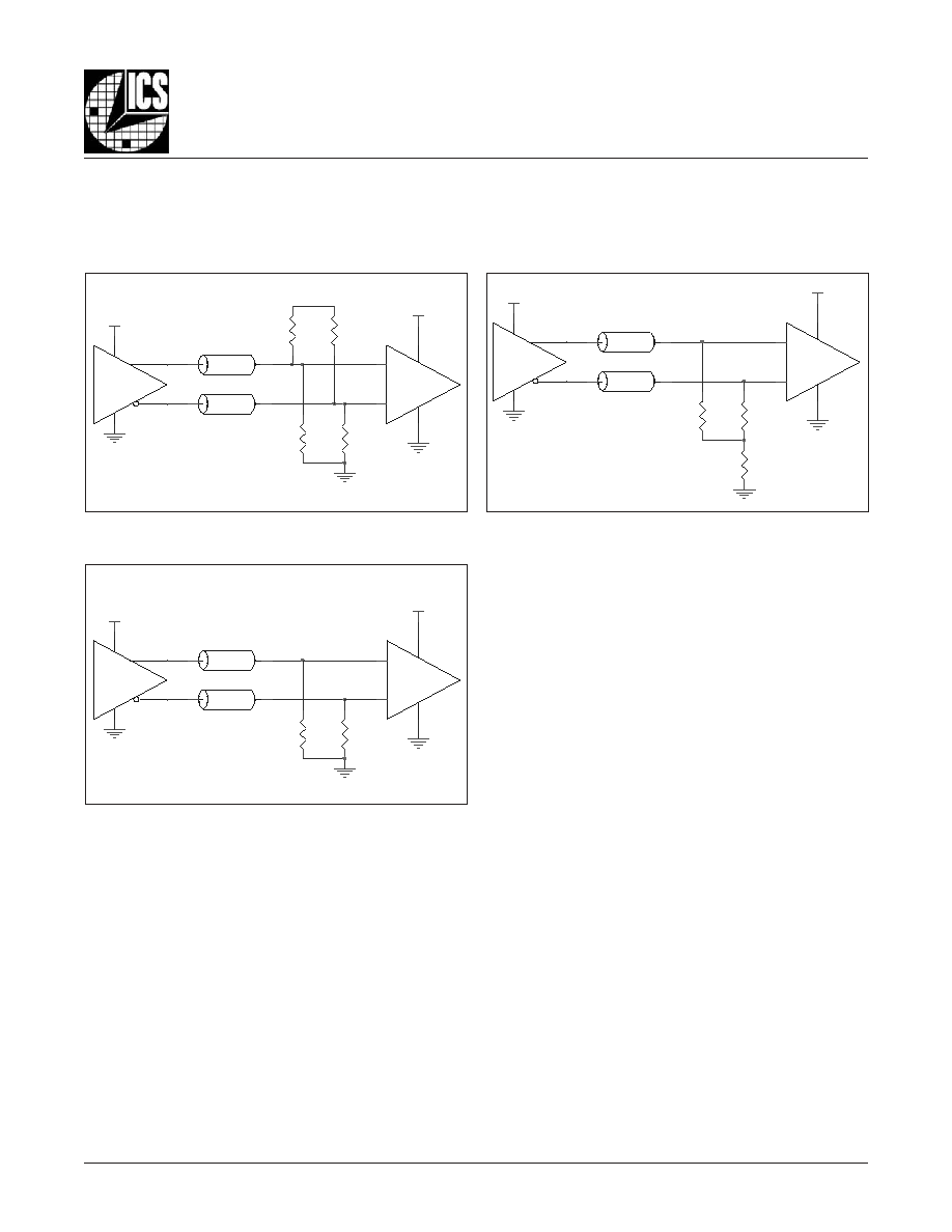
T
ERMINATION
FOR
2.5V LVPECL O
UTPUT
Figure 4A
and
Figure 4B
show examples of termination for
2.5V LVPECL driver. These terminations are equivalent to ter-
minating 50
to V
CC
- 2V. For V
CC
= 2.5V, the V
CC
- 2V is very
close to ground level. The R3 in Figure 4B can be eliminated
and the termination is shown in
Figure 4C.
F
IGURE
4C. 2.5V LVPECL T
ERMINATION
E
XAMPLE
F
IGURE
4B. 2.5V LVPECL D
RIVER
T
ERMINATION
E
XAMPLE
F
IGURE
4A. 2.5V LVPECL D
RIVER
T
ERMINATION
E
XAMPLE
R2
62.5
Zo = 50 Ohm
R1
250
+
-
2.5V
2,5V LVPECL
Driv er
R4
62.5
R3
250
Zo = 50 Ohm
2.5V
VCC=2.5V
R1
50
R3
18
Zo = 50 Ohm
Zo = 50 Ohm
+
-
2,5V LVPECL
Driv er
VCC=2.5V
2.5V
R2
50
2,5V LVPECL
Driv er
VCC=2.5V
R1
50
R2
50
2.5V
Zo = 50 Ohm
Zo = 50 Ohm
+
-

843071AGI
www.icst.com/products/hiperclocks.html
REV. A JANUARY 11, 2006
11
Integrated
Circuit
Systems, Inc.
ICS843071I
F
EMTO
C
LOCKS
TM C
RYSTAL
-
TO
- LVPECL
C
LOCK
G
ENERATOR
P
OWER
C
ONSIDERATIONS
This section provides information on power dissipation and junction temperature for the ICS843071I.
Equations and example calculations are also provided.
1. Power Dissipation.
The total power dissipation for the ICS843071I is the sum of the core power plus the power dissipated in the load(s).
The following is the power dissipation for V
CC
= 3.3V + 10% = 3.63V, which gives worst case results.
NOTE: Please refer to Section 3 for details on calculating power dissipated in the load.
�
Power (core)
MAX
= V
CC_MAX
* I
EE_TYP
= 3.63V * 96mA = 348.5mW
�
Power (outputs)
MAX
= 30mW/Loaded Output pair
Total Power
_MAX
(3.63V, with all outputs switching) = 348.5mW + 30mW = 378.5mW
2. Junction Temperature.
Junction temperature, Tj, is the temperature at the junction of the bond wire and bond pad and directly affects the reliability of the
device. The maximum recommended junction temperature for HiPerClockS
TM
devices is 125�C.
The equation for Tj is as follows: Tj =
JA
* Pd_total + T
A
Tj = Junction Temperature
JA
= Junction-to-Ambient Thermal Resistance
Pd_total = Total Device Power Dissipation (example calculation is in section 1 above)
T
A
= Ambient Temperature
In order to calculate junction temperature, the appropriate junction-to-ambient thermal resistance
JA
must be used. Assuming a
moderate air flow of 1 meter per second and a multi-layer board, the appropriate value is 90.5�C/W per Table 6 below.
Therefore, Tj for an ambient temperature of 85�C with all outputs switching is:
85�C + 0.379W * 90.5�C/W = 119.3�C. This is below the limit of 125�C.
This calculation is only an example. Tj will obviously vary depending on the number of loaded outputs, supply voltage, air flow,
and the type of board (single layer or multi-layer).
T
ABLE
6. T
HERMAL
R
ESISTANCE
JA
FOR
8-
PIN
TSSOP, F
ORCED
C
ONVECTION
JA
by Velocity (Meters per Second)
0
1
2.5
Multi-Layer PCB, JEDEC Standard Test Boards
101.7�C/W
90.5�C/W
89.8�C/W
843071AGI
www.icst.com/products/hiperclocks.html
REV. A JANUARY 11, 2006
12
Integrated
Circuit
Systems, Inc.
ICS843071I
F
EMTO
C
LOCKS
TM C
RYSTAL
-
TO
- LVPECL
C
LOCK
G
ENERATOR
3. Calculations and Equations.
The purpose of this section is to derive the power dissipated into the load.
LVPECL output driver circuit and termination are shown in
Figure 5.
T
o calculate worst case power dissipation into the load, use the following equations which assume a 50
load, and a termination
voltage of V
CC
- 2V.
�
For logic high, V
OUT
= V
OH_MAX
= V
CC_MAX
� 0.9V
(V
CCO_MAX
- V
OH_MAX
) = 0.9V
�
For logic low, V
OUT
= V
OL_MAX
= V
CC_MAX
� 1.7V
(V
CCO_MAX
- V
OL_MAX
) = 1.7V
Pd_H is power dissipation when the output drives high.
Pd_L is the power dissipation when the output drives low.
Pd_H = [(V
OH_MAX
� (V
CC_MAX
- 2V))/R
L
] * (V
CC_MAX
- V
OH_MAX
) = [(2V - (V
CC_MAX
- V
OH_MAX
))/R
L
] * (V
CC_MAX
- V
OH_MAX
) =
[(2V - 0.9V)/50
] * 0.9V = 19.8mW
Pd_L = [(V
OL_MAX
� (V
CC_MAX
- 2V))/R
L
] * (V
CC_MAX
- V
OL_MAX
) = [(2V - (V
CC_MAX
- V
OL_MAX
))/R
L
] * (V
CC_MAX
- V
OL_MAX
) =
[(2V - 1.7V)/50
] * 1.7V = 10.2mW
Total Power Dissipation per output pair = Pd_H + Pd_L = 30mW
F
IGURE
5. LVPECL D
RIVER
C
IRCUIT
AND
T
ERMINATION
Q1
V
OUT
V
CC
RL
50
V
CC
- 2V

843071AGI
www.icst.com/products/hiperclocks.html
REV. A JANUARY 11, 2006
13
Integrated
Circuit
Systems, Inc.
ICS843071I
F
EMTO
C
LOCKS
TM C
RYSTAL
-
TO
- LVPECL
C
LOCK
G
ENERATOR
R
ELIABILITY
I
NFORMATION
T
RANSISTOR
C
OUNT
The transistor count for ICS843071I is: 1732
T
ABLE
7.
JA
VS
. A
IR
F
LOW
T
ABLE
FOR
8 L
EAD
TSSOP
JA
by Velocity (Linear Feet per Minute)
0
1
2.5
Multi-Layer PCB, JEDEC Standard Test Boards
101.7�C/W
90.5�C/W
89.8�C/W
843071AGI
www.icst.com/products/hiperclocks.html
REV. A JANUARY 11, 2006
14
Integrated
Circuit
Systems, Inc.
ICS843071I
F
EMTO
C
LOCKS
TM C
RYSTAL
-
TO
- LVPECL
C
LOCK
G
ENERATOR
P
ACKAGE
O
UTLINE
- G S
UFFIX
FOR
8 L
EAD
TSSOP
T
ABLE
8. P
ACKAGE
D
IMENSIONS
Reference Document: JEDEC Publication 95, MO-153
L
O
B
M
Y
S
s
r
e
t
e
m
i
l
l
i
M
m
u
m
i
n
i
M
m
u
m
i
x
a
M
N
8
A
-
-
0
2
.
1
1
A
5
0
.
0
5
1
.
0
2
A
0
8
.
0
5
0
.
1
b
9
1
.
0
0
3
.
0
c
9
0
.
0
0
2
.
0
D
0
9
.
2
0
1
.
3
E
C
I
S
A
B
0
4
.
6
1
E
0
3
.
4
0
5
.
4
e
C
I
S
A
B
5
6
.
0
L
5
4
.
0
5
7
.
0
�
0
�
8
a
a
a
-
-
0
1
.
0
843071AGI
www.icst.com/products/hiperclocks.html
REV. A JANUARY 11, 2006
15
Integrated
Circuit
Systems, Inc.
ICS843071I
F
EMTO
C
LOCKS
TM C
RYSTAL
-
TO
- LVPECL
C
LOCK
G
ENERATOR
T
ABLE
9. O
RDERING
I
NFORMATION
While the information presented herein has been checked for both accuracy and reliability, Integrated Circuit Systems, Incorporated (ICS) assumes no responsibility for either its use
or for infringement of any patents or other rights of third parties, which would result from its use. No other circuits, patents, or licenses are implied. This product is intended for use
in normal commercial and industrial applications. Any other applications such as those requiring high reliability or other extraordinary environmental requirements are not
recommended without additional processing by ICS. ICS reserves the right to change any circuitry or specifications without notice. ICS does not authorize or warrant any ICS product
for use in life support devices or critical medical instruments.
The aforementioned trademarks, HiPerClockS and FemtoClocks are trademarks of Integrated Circuit Systems, Inc. or its subsidiaries in the United States and/or other countries.
r
e
b
m
u
N
r
e
d
r
O
/
t
r
a
P
g
n
i
k
r
a
M
e
g
a
k
c
a
P
g
n
i
g
a
k
c
a
P
g
n
i
p
p
i
h
S
e
r
u
t
a
r
e
p
m
e
T
I
G
A
1
7
0
3
4
8
S
C
I
A
1
7
0
3
P
O
S
S
T
d
a
e
L
8
e
b
u
t
C
�
5
8
o
t
C
�
0
4
-
T
I
G
A
1
7
0
3
4
8
S
C
I
A
1
7
0
3
P
O
S
S
T
d
a
e
L
8
l
e
e
r
&
e
p
a
t
0
0
5
2
C
�
5
8
o
t
C
�
0
4
-
F
L
I
G
A
1
7
0
3
4
8
S
C
I
D
B
T
P
O
S
S
T
"
e
e
r
F
-
d
a
e
L
"
d
a
e
L
8
e
b
u
t
C
�
5
8
o
t
C
�
0
4
-
T
F
L
I
G
A
1
7
0
3
4
8
S
C
I
D
B
T
P
O
S
S
T
"
e
e
r
F
-
d
a
e
L
"
d
a
e
L
8
l
e
e
r
&
e
p
a
t
0
0
5
2
C
�
5
8
o
t
C
�
0
4
-
.
t
n
a
il
p
m
o
c
S
H
o
R
e
r
a
d
n
a
n
o
i
t
a
r
u
g
i
f
n
o
c
e
e
r
F
-
b
P
e
h
t
e
r
a
r
e
b
m
u
n
t
r
a
p
e
h
t
o
t
x
i
f
f
u
s
"
F
L
"
n
a
h
t
i
w
d
e
r
e
d
r
o
e
r
a
t
a
h
t
s
t
r
a
P
:
E
T
O
N