Document Outline
- General Description
- Features
- Block Diagram
- Pin Assignment
- Functional Description
- Pin Descriptions
- Pin Characteristics
- SSC Control Input Function Table
- Programmable VCO Frequency Function Table
- Absolute Maximum Ratings
- Power Supply DC Characteristics
- LVCMOS DC Characteristics
- LVPECL DC Characteristics
- Crystal Characteristics
- AC Characteristics
- Parameter Measurement Information
- 3.3V Output Load AC Test Circuit Diagram
- Cycle-to-Cycle Jitter Diagram
- Output Rise/Fall Time Diagram
- odc & tPeriod Diagram
- Application Information
- Crystal Input and Oscillator Interface
- Crystal Interface Diagram
- Crystal Frequency Plot
- Series Capacitor Plot
- Spread Sprectrum
- Triangle Frequency Modulation Diagram
- 200MHz Clock Output in Frequency Domain Plot
- Power Supply Filtering Techniques
- Power Supply Filtering Diagram
- Termination for LVPECL Outputs
- LVPECL Output Termination Diagrams
- Layout Guideline
- Recommended Schematic Layout
- Power & Grounding
- Clock Traces & Termination
- Crystal
- PCB Board Layout
- Power Considerations
- Power Dissipation
- Junction Temperature
- Thermal Resistance
- Calculations & Equations
- LVPECL Driver Circuit & Termination
- Reliability Information
- Transistor Count
- Package Outline
- Package Dimensions
- Ordering Information
- Revision History Sheet
8431EM-11
www.icst.com/products/hiperclocks.html
REV. D JUNE 20, 2003
1
Integrated
Circuit
Systems, Inc.
ICS8431-11
255MH
Z
, L
OW
J
ITTER
, C
RYSTAL
O
SCILLATOR
-
TO
-3.3V LVPECL F
REQUENCY
S
YNTHESIZER
G
ENERAL
D
ESCRIPTION
The ICS8431-11 is a general purpose clock fre-
quency synthesizer for IA64/32 application and
a member of the HiPerClockSTM family of High
Performance Clock Solutions from ICS. The VCO
operates at a frequency range of 250MHz to
510MHz providing an output frequency range of 125MHz to
255MHz. The output frequency can be programmed using the
parallel interface, M0 through M8, to the configuration logic.
Spread spectrum clocking is programmed via the control in-
puts SSC_CTL0 and SSC_CTL1.
Programmable features of the ICS8431-11 support four op-
erational modes. The four modes are spread spectrum clock-
ing (SSC), non-spread spectrum clock and two test modes
which are controlled by the SSC_CTL[1:0] pins. Unlike other
synthesizers, the ICS8431-11 can immediately change
spread-spectrum operation without having to reset the device.
In SSC mode, the output clock is modulated in order to achieve
a reduction in EMI. In one of the PLL bypass test modes, the
PLL is disconnected as the source to the differential output
allowing an external source to be connected to the TEST_I/O
pin. This is useful for in-circuit testing and allows the differen-
tial output to be driven at a lower frequency throughout the
system clock tree. In the other PLL bypass mode, the oscilla-
tor divider is used as the source to both the M and the Fout
divide by 2. This is useful for characterizing the oscillator and
internal dividers.
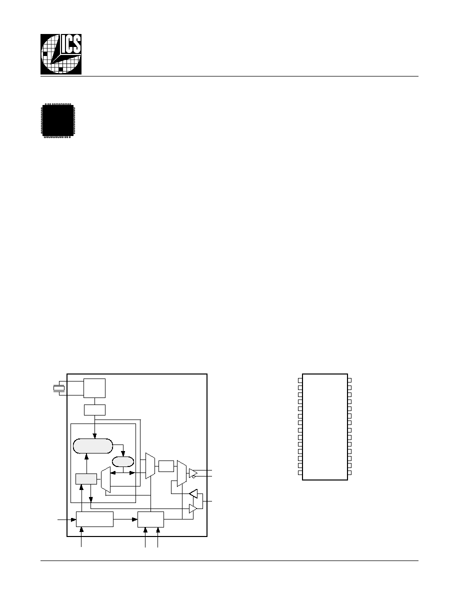
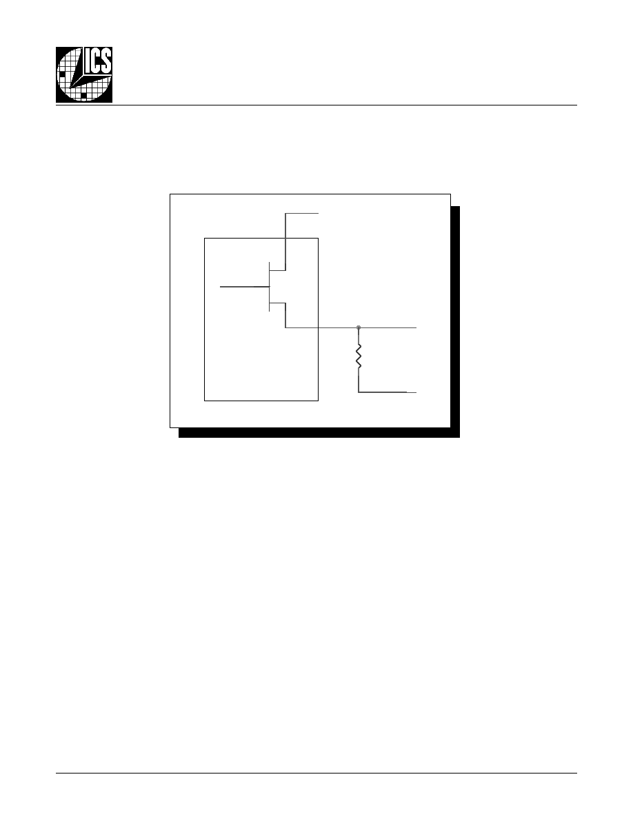
XTAL1
XTAL2
M0:M8
PLL
FOUT
nFOUT
�
16
TEST_I/O
OSC
VCO
�
2
PHASE
DETECTOR
�
M
SSC
Control
Logic
Configuration
Logic
nP_LOAD
SSC_CTL0
F
EATURES
�
Fully integrated PLL
�
Differential 3.3V LVPECL output
�
Crystal oscillator interface
�
Output frequency range: 125MHz to 255MHz
�
Crystal input frequency range: 14MHz to 20MHz
�
VCO range: 250MHz to 510MHz
�
Programmable PLL loop divider for generating a variety
of output frequencies
�
Spread Spectrum Clocking (SSC) fixed at 1/2% modulation
for environments requiring ultra low EMI
�
PLL bypass modes supporting in-circuit testing and on-chip
functional block characterization
�
Cycle-to-cycle jitter: 30ps (maximum)
�
3.3V supply voltage
�
0�C to 85�C ambient operating temperature
B
LOCK
D
IAGRAM
P
IN
A
SSIGNMENT
SSC_CTL1
M0
M1
M2
M3
M4
M5
M6
M7
M8
SSC_CTL0
SSC_CTL1
V
EE
TEST_I/O
V
CC
1
2
3
4
5
6
7
8
9
10
11
12
13
14
28
27
26
25
24
23
22
21
20
19
18
17
16
15
nP_LOAD
V
CC
XTAL2
XTAL1
nc
nc
V
CCA
V
EE
MR
nc
V
CCO
FOUT
nFOUT
V
EE
ICS8431-11
28-Lead SOIC
7.5mm x 18.05mm x 2.25mm package body
M Package
Top View
HiPerClockSTM
,&6

8431EM-11
www.icst.com/products/hiperclocks.html
REV. D JUNE 20, 2003
2
Integrated
Circuit
Systems, Inc.
ICS8431-11
255MH
Z
, L
OW
J
ITTER
, C
RYSTAL
O
SCILLATOR
-
TO
-3.3V LVPECL F
REQUENCY
S
YNTHESIZER
The PLL loop divider or M divider is programmed by using
inputs M0 through M8. While the nP_LOAD input is held LOW,
the data present at M0:M8 is transparent to the M divider. On
the LOW-to-HIGH transition of nP_LOAD, the M0:M8 data is
latched into the M divider and any further changes at the
M0:M8 inputs will not be seen by the M divider until the next
LOW transition on nP_LOAD.
The relationship between the VCO frequency, the crystal fre-
quency and the M divider is defined as follows:
The M value and the required values of M0:M8 for programming
the VCO are shown in
Table 3B, Programmable VCO Frequency
Function Table. The frequency out is defined as follows:
For the ICS8431-11, the output divider equals 2. Valid M val-
ues for which the PLL will achieve lock are defined as:
250
M
510.
F
UNCTIONAL
D
ESCRIPTION
The ICS8431-11 features a fully integrated PLL and therefore
requires no external components for setting the loop bandwidth.
A 16MHz series-resonant, fundamental crystal is used as the
input to the on-chip oscillator. The output of the oscillator is di-
vided by 16 prior to the phase detector. With a 16MHz crystal this
provides a 1MHz reference frequency. The VCO of the PLL oper-
ates over a range of 250MHz to 510MHz. The output of the M
divider is also applied to the phase detector.
The phase detector and the M divider force the VCO output
frequency to be M times the reference frequency by adjusting
the VCO control voltage. Note that for some values of M (ei-
ther too high or too low), the PLL will not achieve lock. The
output of the VCO is scaled by a divider prior to being sent to
the LVPECL output buffer. The divider provides a 50% output
duty cycle.
The programmable features of the ICS8431-11 support four
output operational modes and a programmable M divider and
output divider. The four output operational modes are spread
spectrum clocking (SSC), non-spread spectrum clock and
two test modes and are controlled by the SSC_CTL[1:0] pins.
16
M
fVCO =
fxtal x
2
FOUT =
fVCO
=
32
fxtal x M
8431EM-11
www.icst.com/products/hiperclocks.html
REV. D JUNE 20, 2003
3
Integrated
Circuit
Systems, Inc.
ICS8431-11
255MH
Z
, L
OW
J
ITTER
, C
RYSTAL
O
SCILLATOR
-
TO
-3.3V LVPECL F
REQUENCY
S
YNTHESIZER
T
ABLE
1. P
IN
D
ESCRIPTIONS
T
ABLE
2. P
IN
C
HARACTERISTICS
r
e
b
m
u
N
e
m
a
N
e
p
y
T
n
o
i
t
p
i
r
c
s
e
D
,
4
,
3
,
2
,
1
7
,
6
,
5
6
M
-
0
M
t
u
p
n
I
n
w
o
d
ll
u
P
n
o
i
t
s
i
s
n
a
r
t
H
G
I
H
-
o
t
-
W
O
L
n
o
d
e
h
c
t
a
l
a
t
a
D
.
s
t
u
p
n
i
r
e
d
i
v
i
d
M
.
s
l
e
v
e
l
e
c
a
f
r
e
t
n
i
s
n
i
p
L
T
T
V
L
/
S
O
M
C
V
L
.
t
u
p
n
i
D
A
O
L
_
P
n
f
o
9
,
8
8
M
-
7
M
t
u
p
n
I
p
u
ll
u
P
1
1
,
0
1
,
0
L
T
C
C
S
S
1
L
T
C
C
S
S
t
u
p
n
I
p
u
ll
u
P
.
s
l
e
v
e
l
e
c
a
f
r
e
t
n
i
S
O
M
C
V
L
/
L
T
T
V
L
.
s
n
i
p
l
o
r
t
n
o
c
C
C
S
1
2
,
5
1
,
2
1
V
E
E
r
e
w
o
P
V
ll
a
t
c
e
n
n
o
C
.
s
n
i
p
y
l
p
p
u
s
e
v
i
t
a
g
e
N
E
E
.
d
n
u
o
r
g
d
r
a
o
b
o
t
s
n
i
p
3
1
O
/
I
T
S
E
T
/
t
u
p
n
I
t
u
p
t
u
O
.
e
d
o
m
s
s
a
p
y
b
L
L
P
n
i
t
u
p
n
i
s
a
d
e
m
m
a
r
g
o
r
P
7
2
,
4
1
V
C
C
r
e
w
o
P
.
n
i
p
y
l
p
p
u
s
e
r
o
C
7
1
,
6
1
T
U
O
F
,
T
U
O
F
n
t
u
p
t
u
O
.
s
l
e
v
e
l
e
c
a
f
r
e
t
n
i
L
C
E
P
V
L
V
3
.
3
.
r
e
z
i
s
e
h
t
n
y
s
e
h
t
r
o
f
s
t
u
p
t
u
o
l
a
i
t
n
e
r
e
f
f
i
D
8
1
V
O
C
C
r
e
w
o
P
.
n
i
p
y
l
p
p
u
s
t
u
p
t
u
O
4
2
,
3
2
,
9
1
c
n
d
e
s
u
n
U
.
t
c
e
n
n
o
c
o
N
0
2
R
M
t
u
p
n
I
n
w
o
d
ll
u
P
e
r
a
s
r
e
d
i
v
i
d
l
a
n
r
e
t
n
i
e
h
t
,
H
G
I
H
c
i
g
o
l
n
e
h
W
.
t
e
s
e
R
r
e
t
s
a
M
h
g
i
H
e
v
i
t
c
A
t
u
p
t
u
o
d
e
t
r
e
v
n
i
e
h
t
d
n
a
w
o
l
o
g
o
t
T
U
O
F
t
u
p
t
u
o
e
u
r
t
e
h
t
g
n
i
s
u
a
c
t
e
s
e
r
e
h
t
d
n
a
s
r
e
d
i
v
i
d
l
a
n
r
e
t
n
i
e
h
t
,
W
O
L
c
i
g
o
l
n
e
h
W
.
h
g
i
h
o
g
o
t
T
U
O
F
n
T
d
n
a
M
d
e
d
a
o
l
t
c
e
f
f
e
t
o
n
s
e
o
d
R
M
f
o
n
o
i
t
r
e
s
s
A
.
d
e
l
b
a
n
e
e
r
a
s
t
u
p
t
u
o
.
s
l
e
v
e
l
e
c
a
f
r
e
t
n
i
L
T
T
V
L
/
S
O
M
C
V
L
.
s
e
u
l
a
v
2
2
V
A
C
C
r
e
w
o
P
.
n
i
p
y
l
p
p
u
s
g
o
l
a
n
A
6
2
,
5
2
2
L
A
T
X
,
1
L
A
T
X
t
u
p
n
I
.
t
u
p
t
u
o
e
h
t
s
i
2
L
A
T
X
.
t
u
p
n
i
e
h
t
s
i
1
L
A
T
X
.
e
c
a
f
r
e
t
n
i
r
o
t
a
ll
i
c
s
o
l
a
t
s
y
r
C
8
2
D
A
O
L
_
P
n
t
u
p
n
I
n
w
o
d
ll
u
P
0
M
:
8
M
t
a
t
n
e
s
e
r
p
a
t
a
d
n
e
h
w
s
e
n
i
m
r
e
t
e
D
.
t
u
p
n
i
d
a
o
l
l
e
ll
a
r
a
P
.
s
l
e
v
e
l
e
c
a
f
r
e
t
n
i
S
O
M
C
V
L
/
L
T
T
V
L
.
r
e
d
i
v
i
d
M
o
t
n
i
d
e
d
a
o
l
s
i
:
E
T
O
N
p
u
ll
u
P
d
n
a
n
w
o
d
ll
u
P
.
s
e
u
l
a
v
l
a
c
i
p
y
t
r
o
f
,
s
c
i
t
s
i
r
e
t
c
a
r
a
h
C
n
i
P
,
2
e
l
b
a
T
e
e
S
.
s
r
o
t
s
i
s
e
r
t
u
p
n
i
l
a
n
r
e
t
n
i
o
t
r
e
f
e
r
l
o
b
m
y
S
r
e
t
e
m
a
r
a
P
s
n
o
i
t
i
d
n
o
C
t
s
e
T
m
u
m
i
n
i
M
l
a
c
i
p
y
T
m
u
m
i
x
a
M
s
t
i
n
U
C
N
I
e
c
n
a
t
i
c
a
p
a
C
n
i
P
t
u
p
n
I
4
F
p
R
P
U
L
L
U
P
r
o
t
s
i
s
e
R
p
u
ll
u
P
t
u
p
n
I
1
5
K
R
N
W
O
D
L
L
U
P
r
o
t
s
i
s
e
R
n
w
o
d
ll
u
P
t
u
p
n
I
1
5
K
8431EM-11
www.icst.com/products/hiperclocks.html
REV. D JUNE 20, 2003
4
Integrated
Circuit
Systems, Inc.
ICS8431-11
255MH
Z
, L
OW
J
ITTER
, C
RYSTAL
O
SCILLATOR
-
TO
-3.3V LVPECL F
REQUENCY
S
YNTHESIZER
T
ABLE
3A. SSC C
ONTROL
I
NPUT
F
UNCTION
T
ABLE
T
ABLE
3B. P
ROGRAMMABLE
VCO F
REQUENCY
F
UNCTION
T
ABLE
(NOTE 1)
s
t
u
p
n
I
O
/
I
_
T
S
E
T
e
c
r
u
o
S
C
S
S
s
t
u
p
t
u
O
s
e
d
o
M
l
a
n
o
i
t
a
r
e
p
O
1
L
T
C
_
C
S
S
0
L
T
C
_
C
S
S
,
T
U
O
F
T
U
O
F
n
O
/
I
_
T
S
E
T
0
0
l
a
n
r
e
t
n
I
d
e
l
b
a
s
i
D
L
A
T
X
f
�
2
3
L
A
T
X
f
�
6
1
�
M
t
s
e
t
s
r
e
d
i
v
i
d
N
d
n
a
M
,
r
o
t
a
ll
i
c
s
o
;
s
s
a
p
y
b
L
L
P
1
E
T
O
N
.
e
d
o
m
0
1
L
L
P
d
e
l
b
a
n
E
M
x
L
A
T
X
f
2
3
Z
-
i
H
t
n
e
c
r
e
P
�
=
r
o
t
c
a
F
n
o
i
t
a
l
u
d
o
M
;
C
S
S
t
l
u
a
f
e
D
1
0
l
a
n
r
e
t
x
E
d
e
l
b
a
s
i
D
k
l
C
t
s
e
T
t
u
p
n
I
,
e
d
o
M
s
s
a
p
y
B
L
L
P
z
H
M
1
(
k
l
C
t
s
e
T
1
E
T
O
N
;
)
z
H
M
0
0
2
1
1
L
L
P
d
e
l
b
a
s
i
D
M
x
L
A
T
X
f
2
3
Z
-
i
H
n
o
i
t
a
l
u
d
o
M
C
S
S
o
N
.
n
o
i
t
a
z
i
r
e
t
c
a
r
a
h
c
d
n
a
g
u
b
e
d
e
s
u
o
h
n
i
r
o
f
d
e
s
U
:
1
E
T
O
N
y
c
n
e
u
q
e
r
F
O
C
V
)
z
H
M
(
t
n
u
o
C
M
6
5
2
8
2
1
4
6
2
3
6
1
8
4
2
1
8
M
7
M
6
M
5
M
4
M
3
M
2
M
1
M
0
M
0
5
2
0
5
2
0
1
1
1
1
1
0
1
0
1
5
2
1
5
2
0
1
1
1
1
1
0
1
1
2
5
2
2
5
2
0
1
1
1
1
1
1
0
0
3
5
2
3
5
2
0
1
1
1
1
1
1
0
1
�
�
�
�
�
�
�
�
�
�
�
�
�
�
�
�
�
�
�
�
�
�
8
0
5
8
0
5
1
1
1
1
1
1
1
0
0
9
0
5
9
0
5
1
1
1
1
1
1
1
0
1
0
1
5
0
1
5
1
1
1
1
1
1
1
1
0
.
l
a
t
s
y
r
c
z
H
M
6
1
a
s
e
m
u
s
s
A
:
1
E
T
O
N
8431EM-11
www.icst.com/products/hiperclocks.html
REV. D JUNE 20, 2003
5
Integrated
Circuit
Systems, Inc.
ICS8431-11
255MH
Z
, L
OW
J
ITTER
, C
RYSTAL
O
SCILLATOR
-
TO
-3.3V LVPECL F
REQUENCY
S
YNTHESIZER
T
ABLE
4B. LVCMOS / LVTTL DC C
HARACTERISTICS
,
V
CC
= V
CCA
= V
CCO
= 3.3V�5%, T
A
= 0�C
TO
85�C
T
ABLE
4C. LVPECL DC C
HARACTERISTICS
,
V
CC
= V
CCA
= V
CCO
= 3.3V�5%, T
A
= 0�C
TO
85�C
l
o
b
m
y
S
r
e
t
e
m
a
r
a
P
s
n
o
i
t
i
d
n
o
C
t
s
e
T
m
u
m
i
n
i
M
l
a
c
i
p
y
T
m
u
m
i
x
a
M
s
t
i
n
U
V
H
O
1
E
T
O
N
;
e
g
a
t
l
o
V
h
g
i
H
t
u
p
t
u
O
V
O
C
C
4
.
1
-
V
O
C
C
0
.
1
-
V
V
L
O
e
g
a
t
l
o
V
w
o
L
t
u
p
t
u
O
1
E
T
O
N
;
V
O
C
C
0
.
2
-
V
O
C
C
7
.
1
-
V
V
G
N
I
W
S
g
n
i
w
S
e
g
a
t
l
o
V
t
u
p
t
u
O
k
a
e
P
-
o
t
-
k
a
e
P
0
0
6
0
0
7
0
5
8
V
m
0
5
h
t
i
w
d
e
t
a
n
i
m
r
e
t
t
u
p
t
u
O
:
1
E
T
O
N
V
o
t
O
C
C
.
t
i
u
c
r
i
C
t
s
e
T
d
a
o
L
t
u
p
t
u
O
V
3
.
3
,
n
o
i
t
c
e
S
t
n
e
m
e
r
u
s
a
e
M
r
e
t
e
m
a
r
a
P
e
e
S
.
V
2
-
T
ABLE
4A. P
OWER
S
UPPLY
DC C
HARACTERISTICS
,
V
CC
= V
CCA
= V
CCO
= 3.3V�5%, T
A
= 0�C
TO
85�C
l
o
b
m
y
S
r
e
t
e
m
a
r
a
P
s
n
o
i
t
i
d
n
o
C
t
s
e
T
m
u
m
i
n
i
M
l
a
c
i
p
y
T
m
u
m
i
x
a
M
s
t
i
n
U
V
H
I
e
g
a
t
l
o
V
h
g
i
H
t
u
p
n
I
,
0
L
T
C
_
C
S
S
,
8
M
:
0
M
,
R
M
,
1
L
T
C
_
C
S
S
D
A
O
L
_
P
n
,
O
/
I
_
T
S
E
T
V
5
3
1
.
3
V
C
C
V
5
6
4
.
3
2
V
C
C
3
.
0
+
V
V
L
I
e
g
a
t
l
o
V
w
o
L
t
u
p
n
I
,
0
L
T
C
_
C
S
S
,
8
M
:
0
M
,
R
M
,
1
L
T
C
_
C
S
S
D
A
O
L
_
P
n
,
O
/
I
_
T
S
E
T
V
5
3
1
.
3
V
C
C
V
5
6
4
.
3
3
.
0
-
8
.
0
V
I
H
I
t
n
e
r
r
u
C
h
g
i
H
t
u
p
n
I
,
0
L
T
C
_
C
S
S
,
8
M
,
7
M
O
I
_
T
S
E
T
,
1
L
T
C
_
C
S
S
V
C
C
V
=
N
I
V
5
6
4
.
3
=
5
A
�
,
6
M
:
0
M
R
M
,
D
A
O
L
_
P
n
V
C
C
V
=
N
I
V
5
6
4
.
3
=
0
5
1
A
�
I
L
I
t
n
e
r
r
u
C
w
o
L
t
u
p
n
I
,
0
L
T
C
_
C
S
S
,
8
M
,
7
M
O
I
_
T
S
E
T
,
1
L
T
C
_
C
S
S
V
C
C
V
,
V
5
6
4
.
3
=
N
I
V
0
=
0
5
1
-
A
�
,
6
M
:
0
M
R
M
,
D
A
O
L
_
P
n
V
C
C
V
,
V
5
6
4
.
3
=
N
I
V
0
=
5
-
A
�
l
o
b
m
y
S
r
e
t
e
m
a
r
a
P
s
n
o
i
t
i
d
n
o
C
t
s
e
T
m
u
m
i
n
i
M
l
a
c
i
p
y
T
m
u
m
i
x
a
M
s
t
i
n
U
V
C
C
e
g
a
t
l
o
V
y
l
p
p
u
S
e
r
o
C
5
3
1
.
3
3
.
3
5
6
4
.
3
V
V
O
C
C
e
g
a
t
l
o
V
y
l
p
p
u
S
t
u
p
t
u
O
5
3
1
.
3
3
.
3
5
6
4
.
3
V
V
A
C
C
e
g
a
t
l
o
V
y
l
p
p
u
S
g
o
l
a
n
A
5
3
1
.
3
3
.
3
5
6
4
.
3
V
I
E
E
t
n
e
r
r
u
C
y
l
p
p
u
S
r
e
w
o
P
0
4
1
A
m
NOTE: Stresses beyond those listed under Absolute
Maximum Ratings may cause permanent damage to the
device. These ratings are stress specifications only. Functional
operation of product at these conditions or any conditions be-
yond those listed in the
DC Characteristics or AC Character-
istics is not implied. Exposure to absolute maximum rating
conditions for extended periods may affect product reliability.
A
BSOLUTE
M
AXIMUM
R
ATINGS
Supply Voltage, V
CC
4.6V
Inputs, V
I
-0.5V to V
CC
+ 0.5V
Outputs, I
O
Continuous Current
50mA
Surge Current
100mA
Package Thermal Impedance,
JA
46.2�C/W (0 lfpm)
Storage Temperature, T
STG
-65�C to 150�C
8431EM-11
www.icst.com/products/hiperclocks.html
REV. D JUNE 20, 2003
6
Integrated
Circuit
Systems, Inc.
ICS8431-11
255MH
Z
, L
OW
J
ITTER
, C
RYSTAL
O
SCILLATOR
-
TO
-3.3V LVPECL F
REQUENCY
S
YNTHESIZER
T
ABLE
6. AC C
HARACTERISTICS
,
V
CC
= V
CCA
= V
CCO
= 3.3V�5%, T
A
= 0�C
TO
85�C
T
ABLE
5. C
RYSTAL
C
HARACTERISTICS
r
e
t
e
m
a
r
a
P
s
n
o
i
t
i
d
n
o
C
t
s
e
T
m
u
m
i
n
i
M
l
a
c
i
p
y
T
m
u
m
i
x
a
M
s
t
i
n
U
n
o
i
t
a
ll
i
c
s
O
f
o
e
d
o
M
l
a
t
n
e
m
a
d
n
u
F
y
c
n
e
u
q
e
r
F
0
.
6
1
z
H
M
)
R
S
E
(
e
c
n
a
t
s
i
s
e
R
s
e
i
r
e
S
t
n
e
l
a
v
i
u
q
E
0
4
e
c
n
a
t
i
c
a
p
a
C
t
n
u
h
S
3
7
F
p
l
o
b
m
y
S
r
e
t
e
m
a
r
a
P
s
n
o
i
t
i
d
n
o
C
t
s
e
T
m
u
m
i
n
i
M
l
a
c
i
p
y
T
m
u
m
i
x
a
M
s
t
i
n
U
F
e
v
a
1
E
T
O
N
;
y
c
n
e
u
q
e
r
F
t
u
p
t
u
O
e
g
a
r
e
v
A
0
5
7
-
0
5
7
+
m
p
p
t
j
)
c
c
(
t
i
6
,
2
E
T
O
N
;
r
e
t
t
i
J
e
l
c
y
C
-
o
t
-
e
l
c
y
C
F
T
U
O
z
H
M
0
0
2
=
8
1
0
3
s
p
5
3
s
p
c
d
o
e
l
c
y
C
y
t
u
D
t
u
p
t
u
O
7
4
3
5
%
t
R
e
m
i
T
e
s
i
R
t
u
p
t
u
O
%
0
8
o
t
%
0
2
0
0
3
0
5
4
0
0
6
s
p
t
F
e
m
i
T
ll
a
F
t
u
p
t
u
O
%
0
8
o
t
%
0
2
0
0
3
0
5
4
0
0
6
s
p
F
l
a
t
x
4
,
3
E
T
O
N
;
e
g
n
a
R
t
u
p
n
I
l
a
t
s
y
r
C
4
1
6
1
0
2
z
H
M
F
M
5
E
T
O
N
;
y
c
n
e
u
q
e
r
F
n
o
i
t
a
l
u
d
o
M
C
S
S
0
3
3
3
.
3
3
z
H
K
F
F
M
5
E
T
O
N
;
r
o
t
c
a
F
n
o
i
t
a
l
u
d
o
M
C
S
S
4
.
0
6
.
0
%
C
S
S
d
e
r
;
n
o
i
t
c
u
d
e
R
l
a
r
t
c
e
p
S
5
E
T
O
N
7
0
1
B
d
t
E
L
B
A
T
S
t
u
p
t
u
O
k
c
o
l
C
e
l
b
a
t
S
o
t
p
u
-
r
e
w
o
P
0
1
s
m
.
n
o
i
t
c
e
s
n
o
i
t
a
m
r
o
f
n
I
t
n
e
m
e
r
u
s
a
e
M
r
e
t
e
m
a
r
a
P
e
h
t
n
i
s
e
r
u
g
i
F
e
e
S
:
1
E
T
O
N
.
s
t
n
e
n
o
p
m
o
c
l
a
t
s
y
r
c
l
a
n
r
e
t
x
e
t
u
o
h
t
i
W
.
s
t
u
p
n
i
L
A
T
X
g
n
i
s
u
e
c
n
a
m
r
o
f
r
e
p
r
e
t
t
i
J
:
2
E
T
O
N
.
e
g
n
a
r
g
n
i
t
a
r
e
p
o
O
C
V
e
h
t
n
i
h
t
i
w
d
il
a
v
y
l
n
O
:
3
E
T
O
N
.
e
t
o
N
n
o
i
t
a
c
il
p
p
A
o
t
r
e
f
e
r
,
t
u
p
n
i
L
A
T
X
r
o
F
:
4
E
T
O
N
:
5
E
T
O
N
.
d
e
l
b
a
n
e
g
n
i
k
c
o
l
c
m
u
r
t
c
e
p
S
d
a
e
r
p
S
.
5
6
d
r
a
d
n
a
t
S
C
E
D
E
J
h
t
i
w
e
c
n
a
d
r
o
c
c
a
n
i
d
e
n
i
f
e
d
s
i
r
e
t
e
m
a
r
a
p
s
i
h
T
:
6
E
T
O
N
8431EM-11
www.icst.com/products/hiperclocks.html
REV. D JUNE 20, 2003
7
Integrated
Circuit
Systems, Inc.
ICS8431-11
255MH
Z
, L
OW
J
ITTER
, C
RYSTAL
O
SCILLATOR
-
TO
-3.3V LVPECL F
REQUENCY
S
YNTHESIZER
P
ARAMETER
M
EASUREMENT
I
NFORMATION
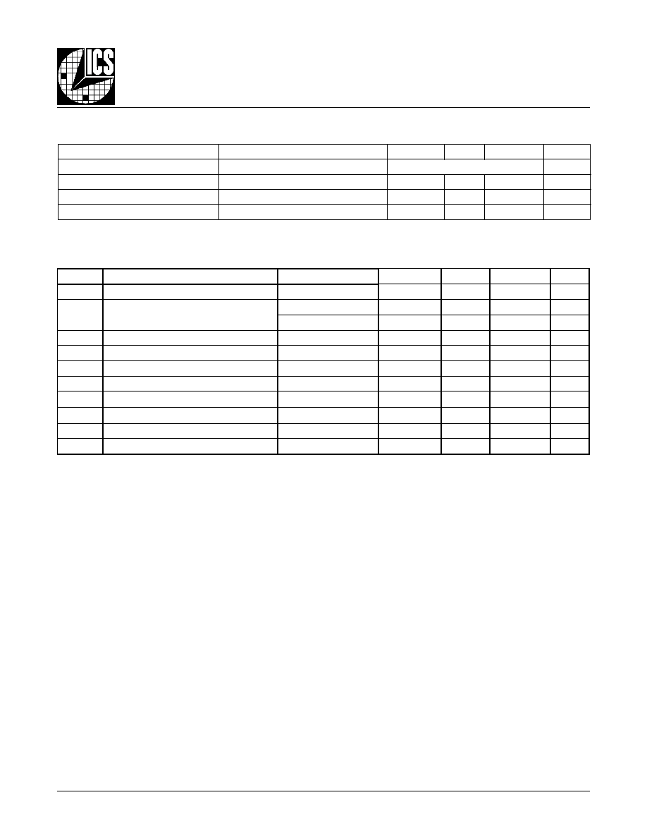
O
UTPUT
R
ISE
/F
ALL
T
IME
3.3V O
UTPUT
L
OAD
AC T
EST
C
IRCUIT
SCOPE
Qx
nQx
LVPECL
V
CC
, V
CCA
, V
CCO
= 2V
odc & t
P
ERIOD
t
jit(cc) =
t
cycle n �
t
cycle n+1
1000 Cycles
t
cycle n
t
cycle n+1
V
EE
= -1.3V � 0.165V
nFOUT
FOUT
Clock
Outputs
20%
80%
80%
20%
t
R
t
F
V
SW I N G
Pulse Width
t
PERIOD
t
PW
t
PERIOD
odc =
FOUT
nFOUT
C
YCLE
-
TO
-C
YCLE
J
ITTER

8431EM-11
www.icst.com/products/hiperclocks.html
REV. D JUNE 20, 2003
8
Integrated
Circuit
Systems, Inc.
ICS8431-11
255MH
Z
, L
OW
J
ITTER
, C
RYSTAL
O
SCILLATOR
-
TO
-3.3V LVPECL F
REQUENCY
S
YNTHESIZER
The ICS8431-11 features an internal oscillator that uses an
external quartz crystal as the source of its reference frequency.
A 16MHz crystal divided by 16 before being sent to the phase
detector provides the reference frequency. The oscillator is a
series resonant, multi-vibrator type design. This design provides
better stability and eliminates the need for large on chip capacitors.
Though a series resonant crystal is preferred, a parallel resonant
crystal can be used. A parallel resonant mode crystal used in a
series resonant circuit will exhibit a frequency of oscillation a few
hundred ppm lower than specified. A few hundred ppm translates
to KHz inaccuracy. In general computing applications this level
of inaccuracy is irrelevant. If better ppm accuracy is required, an
external capacitor can be added to a parallel resonant crystal in
series to pin 25.
Figure 1A shows how to interface with a crystal.
Figures 1A, 1B, and 1C show various crystal parameters which
are recommended only as guidelines.
Figure 1A shows how to
interface a capacitor with an 18pF parallel resonant crystal.
Fig-
ure 1B shows the capacitor value needed for the optimum ppm
performance over various parallel resonant crystals.
Figure 1C
shows the recommended tuning capacitance for a various par-
allel resonant crystal.
F
IGURE
1A. C
RYSTAL
I
NTERFACE
Optional
XTAL2
(Pin 26, SOIC)
XTAL1
(Pin 25, SOIC)
ICS8431-11
F
IGURE
1B. Recommended tuning capacitance for various
18pF parallel resonant crystals.
F
IGURE
1C. Recommended tuning capacitance for various
18pF parallel resonant crystals.
14.318
15.000
16.667
24.000
19.440
20.000
0
10
20
30
40
50
60
14
15
16
17
18
19
20
21
22
23
24
25
Crystal Frequency (MHz)
S
e
r
i
es
C
apac
itor
, C
1
(
p
F
)
-100
-80
-60
-40
-20
0
20
40
60
80
100
0
10
20
30
40
50
60
Series Capacitor, C1 (pF)
F
r
equency A
ccur
a
cy (
ppm
)
19.44MHz
16MHz
15.00MHz
C
RYSTAL
I
NPUT
AND
O
SCILLATOR
I
NTERFACE
�
A
PPLICATION
I
NFORMATION
8431EM-11
www.icst.com/products/hiperclocks.html
REV. D JUNE 20, 2003
9
Integrated
Circuit
Systems, Inc.
ICS8431-11
255MH
Z
, L
OW
J
ITTER
, C
RYSTAL
O
SCILLATOR
-
TO
-3.3V LVPECL F
REQUENCY
S
YNTHESIZER
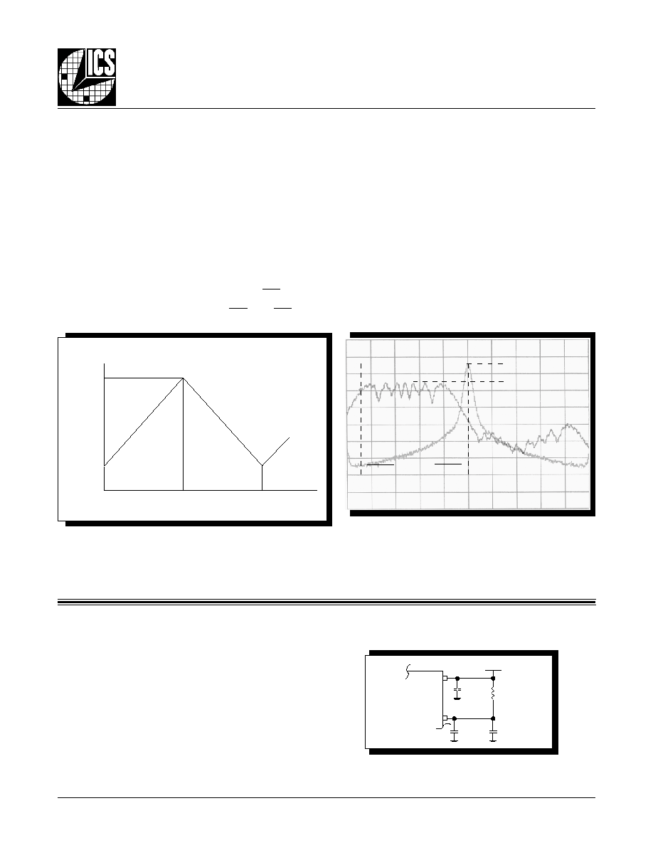
Spread-spectrum clocking is a frequency modulation tech-
nique for EMI reduction. When spread-spectrum is enabled, a
30KHz triangle waveform is used with 0.5% down-spread
(+0.0% / -0.5%) from the nominal 200MHz clock frequency.
An example of a triangle frequency modulation profile is shown
in
Figure 2A below. The ramp profile can be expressed as:
� Fnom = Nominal Clock Frequency in Spread OFF mode
(200MHz with 16MHz IN)
� Fm = Nominal Modulation Frequency (30KHz)
�
= Modulation Factor (0.5% down spread)
(1 -
) fnom + 2 fm x
x fnom x t when 0 < t <
,
(1 -
) fnom - 2 fm x
x fnom x t when
< t <
1
2 fm
1
2 fm
1
fm
The ICS8431-11 triangle modulation frequency deviation will
not exceed 0.6% down-spread from the nominal clock fre-
quency (+0.0% / -0.5%). An example of the amount of down
spread relative to the nominal clock frequency can be seen in
the frequency domain, as shown in
Figure 2B. The ratio of this
width to the fundamental frequency is typically 0.4%, and will
not exceed 0.6%. The resulting spectral reduction will be
greater than 7dB, as shown in Figure 2B. It is important to
note the ICS8431-11 7dB minimum spectral reduction is the
component-specific EMI reduction, and will not necessarily
be the same as the system EMI reduction.
As in any high speed analog circuitry, the power supply pins
are vulnerable to random noise. The ICS8431-11 provides
separate power supplies to isolate any high switching noise
from the outputs to the internal PLL. V
CC
, V
CCA
, and V
CCO
should
be individually connected to the power supply plane through
vias, and bypass capacitors should be used for each pin. To
achieve optimum jitter performance, better power supply iso-
lation is required.
Figure 3 illustrates how a 10
along with a
10
�
F and a .01
�
F bypass capacitor should be connected to
each V
CCA
pin.
F
IGURE
2B. 200MH
Z
C
LOCK
O
UTPUT
IN
F
REQUENCY
D
OMAIN
(A) S
PREAD
-S
PECTRUM
OFF
(B) S
PREAD
-S
PECTRUM
ON
F
IGURE
2A. T
RIANGLE
F
REQUENCY
M
ODULATION
F
IGURE
3. P
OWER
S
UPPLY
F
ILTERING
10
V
CCA
10
�
F
.01
�
F
3.3V
.01
�
F
V
CC
S
PREAD
S
PECTRUM
P
OWER
S
UPPLY
F
ILTERING
T
ECHNIQUES
-
10 dBm
= .4%
B
A
Fnom
(1 -
) Fnom
0.5/fm
1/fm
8431EM-11
www.icst.com/products/hiperclocks.html
REV. D JUNE 20, 2003
10
Integrated
Circuit
Systems, Inc.
ICS8431-11
255MH
Z
, L
OW
J
ITTER
, C
RYSTAL
O
SCILLATOR
-
TO
-3.3V LVPECL F
REQUENCY
S
YNTHESIZER
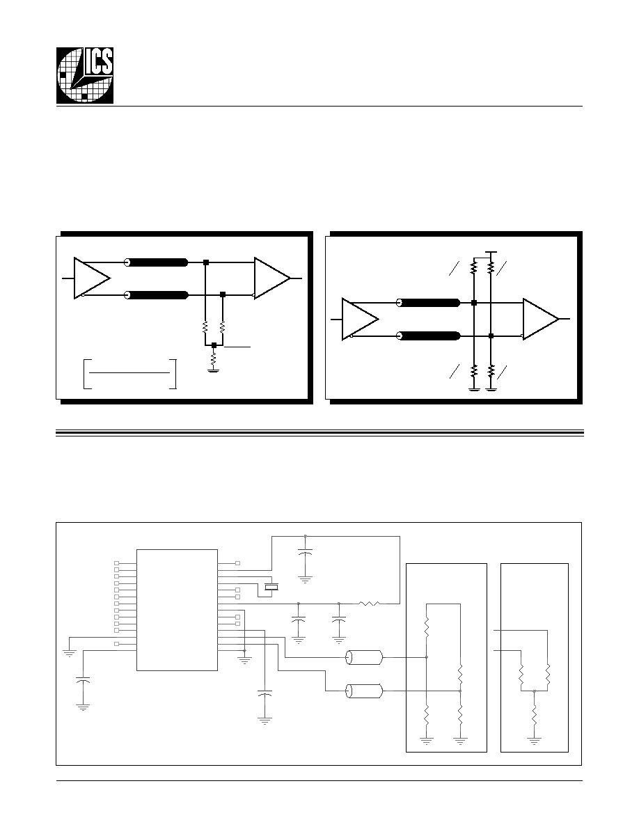
The clock layout topology shown below is typical for
IA64/32 platforms. The two different layouts mentioned are
recommended only as guidelines.
FOUT and nFOUT are low impedance follower outputs that
generate ECL/LVPECL compatible outputs. Therefore, terminat-
ing resistors (DC current path to ground) or current sources
must be used for functionality. These outputs are designed to
F
IGURE
4B. LVPECL O
UTPUT
T
ERMINATION
3.3V
FOUT
FIN
5
2 Z
o
Z
o
5
2
Z
o
3
2
Z
o
3
2
Z
o
= 50
Z
o
= 50
F
IGURE
4A. LVPECL O
UTPUT
T
ERMINATION
RTT =
1
(V
OH
+ V
OL
/ V
CC
�2) �2
Z
o
Z
o
= 50
Z
o
= 50
50
50
RTT
V
CC
-2V
FIN
FOUT
F
IGURE
5A. R
ECOMMENDED
S
CHEMATIC
L
AYOUT
drive 50
transmission lines. Matched impedance techniques
should be used to maximize operating frequency and minimize
signal distortion.
Figures 4A and 4B show two different layouts
which are recommended only as guidelines. Other suitable clock
layouts may exist and it would be recommended that the board
designers simulate to guarantee compatibility across all printed
circuit and clock component process variations.
The schematic of the ICS8431-11 layout example used in this
layout guideline is shown in
Figure 5A. The ICS8431-11 rec-
ommended PCB board layout for this example is shown in
Figure 5B. This layout example is used as a general guide-
VCC
VCC
C4
10uF
IN-
R1
50
VCCA
R1
125
C1
0.1uF
IN+
R2
84
VCC0
C6
0.01uF
TL1
Zo = 50 Ohm
VCC
U1
8431-11
1
2
3
4
5
6
7
8
9
10
11
12
13
14
15
16
17
18
19
20
21
22
23
24
28
27
26
25
M0
M1
M2
M3
M4
M5
M6
M7
M8
SSC_CTL0
SSC_CTL1
VEE
TEST_IO
VCC
VEE
nFOUT
FOUT
VCCO
NC
MR
VEE
VCCA
NC
NC
nP_LOAD
VCC
XTAL1
XTAL2
Termination
B (not shown
in the layout)
R3
50
C3
0.01uF
R5
10
IN+
TL2
Zo = 50 Ohm
C2
0.1uF
X1
R3
125
Termination A
R2
50
IN-
R4
84
L
AYOUT
G
UIDELINE
T
ERMINATION
FOR
LVPECL O
UTPUTS
line. The layout in the actual system will depend on the se-
lected component types, the density of the components, the
density of the traces, and the stack up of the P.C. board.

8431EM-11
www.icst.com/products/hiperclocks.html
REV. D JUNE 20, 2003
11
Integrated
Circuit
Systems, Inc.
ICS8431-11
255MH
Z
, L
OW
J
ITTER
, C
RYSTAL
O
SCILLATOR
-
TO
-3.3V LVPECL F
REQUENCY
S
YNTHESIZER
F
IGURE
5B. PCB B
OARD
L
AYOUT
F
OR
ICS8431-11
R5
VIA
ICS8431-11
C4
IN+
TL1 (50 Ohm)
C6
IN-
R2
R4
R3
VCC
Close to the input
pins of the
receiver
X1
Signals
TL2 (50 Ohm)
R1
C3
C1
C2
GND
U1
The following component footprints are used in this layout
example:
All the resistors and capacitors are size 0603.
P
OWER
AND
G
ROUNDING
Place the decoupling capacitors C1, C2, C3, C4, and C6, as
close as possible to the power pins. If space allows, placment of
the decoupling capacitor on the component side is preferred. This
can reduce unwanted inductance between the decoupling ca-
pacitor and the power pin generated by the via.
Maximize the power and ground pad sizes and number of vias
capacitors. This can reduce the inductance between the power
and ground planes and the component power and ground pins.
The RC filter consisting of R5, C3, and C4 should be placed as
close to the V
CCA
pin as possible.
C
LOCK
T
RACES
AND
T
ERMINATION
Poor signal integrity can degrade the system performance or
cause system failure. In synchronous high-speed digital systems,
the clock signal is less tolerant to poor signal integrity than other
signals. Any ringing on the rising or falling edge or excessive ring
back can cause system failure. The shape of the trace and the
trace delay might be restricted by the available space on the board
and the component location. While routing the traces, the clock
signal traces should be routed first and should be locked prior to
routing other signal traces.
� The differential 50
output traces should have same
length.
� Avoid sharp angles on the clock trace. Sharp angle turns
cause the characteristic impedance to change on the
transmission lines.
� Keep the clock traces on the same layer. Whenever pos-
sible, avoid placing vias on the clock traces. Placement
of vias on the traces can affect the trace characteristic
impedance and hence degrade signal integrity.
� To prevent cross talk, avoid routing other signal traces in
parallel with the clock traces. If running parallel traces is
unavoidable, allow a separation of at least three trace
widths between the differential clock trace and the other
signal trace.
� Make sure no other signal traces are routed between the
clock trace pair.
� The matching termination resistors should be located as
close to the receiver input pins as possible.
The matching termination resistors R1, R2, R3 and R4 should
be located as close to the receiver input pins as possible.
Other termination scheme can also be used but is not shown
in the example.
C
RYSTAL
The crystal X1 should be located as close as possible to the pins
25 (XTAL1) and 26 (XTAL2). The trace length between the X1
and U1 should be kept to a minimum to avoid unwanted parasitic
inductance and capacitance. Other signal traces should not be
routed near the crystal traces.

8431EM-11
www.icst.com/products/hiperclocks.html
REV. D JUNE 20, 2003
12
Integrated
Circuit
Systems, Inc.
ICS8431-11
255MH
Z
, L
OW
J
ITTER
, C
RYSTAL
O
SCILLATOR
-
TO
-3.3V LVPECL F
REQUENCY
S
YNTHESIZER
P
OWER
C
ONSIDERATIONS
This section provides information on power dissipation and junction temperature for the ICS8431-11.
Equations and example calculations are also provided.
1. Power Dissipation.
The total power dissipation for the ICS8431-11 is the sum of the core power plus the power dissipated in the load(s).
The following is the power dissipation for V
CC
= 3.3V + 5% = 3.465V, which gives worst case results.
NOTE: Please refer to Section 3 for details on calculating power dissipated in the load.
�
Power (core)
MAX
= V
CC_MAX
* I
EE_MAX
= 3.465V * 140mA = 485.1mW
�
Power (outputs)
MAX
= 30.2mW/Loaded Output pair
If all outputs are loaded, the total power is 1 * 30.2mW = 30.2mW
Total Power
_MAX
(3.465V, with all outputs switching) = 485.1mW + 30.2mW = 515.3mW
2. Junction Temperature.
Junction temperature, Tj, is the temperature at the junction of the bond wire and bond pad and directly affects the reliability of the
device. The maximum recommended junction temperature for HiPerClockS
TM
devices is 125�C.
The equation for Tj is as follows: Tj =
JA
* Pd_total + T
A
Tj = Junction Temperature
JA
= Junction-to-Ambient Thermal Resistance
Pd_total = Total Device Power Dissipation (example calculation is in section 1 above)
T
A
= Ambient Temperature
In order to calculate junction temperature, the appropriate junction-to-ambient thermal resistance
JA
must be used. Assuming a
moderate air flow of 200 linear feet per minute and a multi-layer board, the appropriate value is 39.7�C/W per Table 7 below.
Therefore, Tj for an ambient temperature of 85�C with all outputs switching is:
85�C + 0.515W * 39.7�C/W = 105.4�C. This is below the limit of 125�C.
This calculation is only an example. Tj will obviously vary depending on the number of loaded outputs, supply voltage, air flow,
and the type of board (single layer or multi-layer).
q
JA
by Velocity (Linear Feet per Minute)
0
200
500
Single-Layer PCB, JEDEC Standard Test Boards
76.2�C/W
60.8�C/W
53.2�C/W
Multi-Layer PCB, JEDEC Standard Test Boards
46.2�C/W
39.7�C/W
36.8�C/W
NOTE: Most modern PCB designs use multi-layered boards. The data in the second row pertains to most designs.
Table 7. T
HERMAL
R
ESISTANCE
q
JA
FOR
28-
PIN
SOIC, F
ORCED
C
ONVECTION
8431EM-11
www.icst.com/products/hiperclocks.html
REV. D JUNE 20, 2003
13
Integrated
Circuit
Systems, Inc.
ICS8431-11
255MH
Z
, L
OW
J
ITTER
, C
RYSTAL
O
SCILLATOR
-
TO
-3.3V LVPECL F
REQUENCY
S
YNTHESIZER
3. Calculations and Equations.
The purpose of this section is to derive the power dissipated into the load.
LVPECL output driver circuit and termination are shown in
Figure 6.
T
o calculate worst case power dissipation into the load, use the following equations which assume a 50
load, and a termination
voltage of V
CCO
- 2V.
�
For logic high, V
OUT
= V
OH_MAX
= V
CCO_MAX
� 1.0V
(V
CCO_MAX
- V
OH_MAX
) = 1.0V
�
For logic low, V
OUT
= V
OL_MAX
= V
CCO_MAX
� 1.7V
(V
CCO_MAX
- V
OL_MAX
) = 1.7V
Pd_H is power dissipation when the output drives high.
Pd_L is the power dissipation when the output drives low.
Pd_H = [(V
OH_MAX
� (V
CCO_MAX
- 2V))/R
L
] * (V
CCO_MAX
- V
OH_MAX
) = [(2V - (V
CCO_MAX
- V
OH_MAX
))/R
L
] * (V
CCO_MAX
- V
OH_MAX
) =
[(2V - 1V)/50
] * 1V = 20.0mW
Pd_L = [(V
OL_MAX
� (V
CCO_MAX
- 2V))/R
L
] * (V
CCO_MAX
- V
OL_MAX
) = [(2V - (V
CCO_MAX
- V
OL_MAX
))/R
L
] * (V
CCO_MAX
- V
OL_MAX
) =
[(2V - 1.7V)/50
] * 1.7V = 10.2mW
Total Power Dissipation per output pair = Pd_H + Pd_L = 30.2mW
F
IGURE
6. LVPECL D
RIVER
C
IRCUIT
AND
T
ERMINATION
Q1
V
OUT
V
CCO
R L
50
V
CCO
- 2V

8431EM-11
www.icst.com/products/hiperclocks.html
REV. D JUNE 20, 2003
14
Integrated
Circuit
Systems, Inc.
ICS8431-11
255MH
Z
, L
OW
J
ITTER
, C
RYSTAL
O
SCILLATOR
-
TO
-3.3V LVPECL F
REQUENCY
S
YNTHESIZER
R
ELIABILITY
I
NFORMATION
T
RANSISTOR
C
OUNT
The transistor count for ICS8431-11 is: 5555
T
ABLE
8.
JA
VS
. A
IR
F
LOW
T
ABLE
q
JA
by Velocity (Linear Feet per Minute)
0
200
500
Single-Layer PCB, JEDEC Standard Test Boards
76.2�C/W
60.8�C/W
53.2�C/W
Multi-Layer PCB, JEDEC Standard Test Boards
46.2�C/W
39.7�C/W
36.8�C/W
NOTE: Most modern PCB designs use multi-layered boards. The data in the second row pertains to most designs.
8431EM-11
www.icst.com/products/hiperclocks.html
REV. D JUNE 20, 2003
15
Integrated
Circuit
Systems, Inc.
ICS8431-11
255MH
Z
, L
OW
J
ITTER
, C
RYSTAL
O
SCILLATOR
-
TO
-3.3V LVPECL F
REQUENCY
S
YNTHESIZER
P
ACKAGE
O
UTLINE
- M S
UFFIX
T
ABLE
9. P
ACKAGE
D
IMENSIONS
Reference Document: JEDEC Publication 95, MS-013, MO-119
L
O
B
M
Y
S
s
r
e
t
e
m
i
l
l
i
M
M
U
M
I
N
I
M
M
U
M
I
X
A
M
N
8
2
A
-
-
5
6
.
2
1
A
0
1
.
0
-
-
2
A
5
0
.
2
5
5
.
2
B
3
3
.
0
1
5
.
0
C
8
1
.
0
2
3
.
0
D
0
7
.
7
1
0
4
.
8
1
E
0
4
.
7
0
6
.
7
e
C
I
S
A
B
7
2
.
1
H
0
0
.
0
1
5
6
.
0
1
h
5
2
.
0
5
7
.
0
L
0
4
.
0
7
2
.
1
�
0
�
8
8431EM-11
www.icst.com/products/hiperclocks.html
REV. D JUNE 20, 2003
16
Integrated
Circuit
Systems, Inc.
ICS8431-11
255MH
Z
, L
OW
J
ITTER
, C
RYSTAL
O
SCILLATOR
-
TO
-3.3V LVPECL F
REQUENCY
S
YNTHESIZER
T
ABLE
10. O
RDERING
I
NFORMATION
While the information presented herein has been checked for both accuracy and reliability, Integrated Circuit Systems, Incorporated (ICS) assumes no responsibility for either its use
or for infringement of any patents or other rights of third parties, which would result from its use. No other circuits, patents, or licenses are implied. This product is intended for use
in normal commercial applications. Any other applications such as those requiring extended temperature range, high reliability, or other extraordinary environmental requirements are
not recommended without additional processing by ICS. ICS reserves the right to change any circuitry or specifications without notice. ICS does not authorize or warrant any ICS
product for use in life support devices or critical medical instruments.
r
e
b
m
u
N
r
e
d
r
O
/
t
r
a
P
g
n
i
k
r
a
M
e
g
a
k
c
a
P
t
n
u
o
C
e
r
u
t
a
r
e
p
m
e
T
1
1
-
M
E
1
3
4
8
S
C
I
1
1
-
M
E
1
3
4
8
S
C
I
C
I
O
S
d
a
e
L
8
2
e
b
u
T
r
e
P
6
2
C
�
5
8
o
t
C
�
0
T
1
1
-
M
E
1
3
4
8
S
C
I
1
1
-
M
E
1
3
4
8
S
C
I
l
e
e
R
d
n
a
e
p
a
T
n
o
C
I
O
S
d
a
e
L
8
2
0
0
0
1
C
�
5
8
o
t
C
�
0
8431EM-11
www.icst.com/products/hiperclocks.html
REV. D JUNE 20, 2003
17
Integrated
Circuit
Systems, Inc.
ICS8431-11
255MH
Z
, L
OW
J
ITTER
, C
RYSTAL
O
SCILLATOR
-
TO
-3.3V LVPECL F
REQUENCY
S
YNTHESIZER
T
E
E
H
S
Y
R
O
T
S
I
H
N
O
I
S
I
V
E
R
v
e
R
e
l
b
a
T
e
g
a
P
e
g
n
a
h
C
f
o
n
o
i
t
p
i
r
c
s
e
D
e
t
a
D
A
1
T
6
T
2
6
.
e
l
b
a
t
n
o
i
t
p
i
r
c
s
e
D
n
i
P
n
i
s
n
o
i
t
p
i
r
c
s
e
d
d
e
s
i
v
e
R
.
e
l
b
a
t
s
c
i
t
s
i
r
e
t
c
a
r
a
h
C
C
A
n
i
s
e
t
o
n
d
e
s
i
v
e
R
V
d
e
g
n
a
h
C
x
D
D
V
o
t
x
C
C
.
t
e
e
h
s
a
t
a
d
t
u
o
h
g
u
o
r
h
t
.
s
e
r
u
g
i
F
d
e
t
a
d
p
U
.
s
n
o
i
t
a
r
e
d
i
s
n
o
C
r
e
w
o
P
d
e
d
d
A
1
0
/
8
1
/
2
1
B
C
4
T
5
T
5
6
V
H
O
V
m
o
r
f
d
e
s
i
v
e
r
s
r
e
t
e
m
a
r
a
p
O
C
C
V
,
.
n
i
M
8
2
.
1
-
O
C
C
o
t
.
x
a
M
8
9
.
0
-
V
O
C
C
V
,
.
n
i
M
V
4
.
1
-
O
C
C
.
x
a
M
V
0
.
1
-
.
d
e
n
e
t
r
o
h
s
n
e
e
b
s
a
h
e
l
b
a
t
s
c
i
t
s
i
r
e
t
c
a
r
a
h
C
l
a
t
s
y
r
C
0
5
m
o
r
f
d
e
g
n
a
h
c
e
u
l
a
v
,
w
o
r
R
S
E
0
7
o
t
.
x
a
M
.
x
a
M
2
0
/
0
1
/
1
B
1
T
3
9
.
e
l
b
a
T
n
o
i
t
p
i
r
c
s
e
D
n
i
P
d
e
t
a
d
p
U
.
t
u
p
n
i
l
a
t
s
y
r
C
n
o
t
x
e
t
o
t
n
o
i
t
p
i
r
c
s
e
d
F
p
8
1
d
e
d
d
A
2
0
/
2
2
/
2
B
1
T
3
.
e
l
b
a
T
n
o
i
t
p
i
r
c
s
e
D
n
i
P
n
i
s
n
i
p
8
M
:
0
M
r
o
f
t
n
e
m
e
c
a
l
p
r
e
b
m
u
n
n
i
p
d
e
t
c
e
r
r
o
C
2
0
/
4
/
3
B
1
T
3
.
n
i
p
R
M
r
o
f
n
o
i
t
p
i
r
c
s
e
d
d
e
t
c
e
r
r
o
c
,
e
l
b
a
T
n
o
i
t
p
i
r
c
s
e
D
n
i
P
2
0
/
6
/
6
B
1
T
3
V
r
o
f
n
o
i
t
p
i
r
c
s
e
d
d
e
t
c
e
r
r
o
c
,
e
l
b
a
T
n
o
i
t
p
i
r
c
s
e
D
n
i
P
E
E
.
n
i
p
2
0
/
8
1
/
6
B
1
o
t
m
p
p
0
5
7
-
:
e
g
n
a
r
y
c
n
e
u
q
e
r
f
t
u
p
t
u
o
e
g
a
r
e
v
A
"
d
e
c
a
l
p
e
r
,
n
o
i
t
c
e
s
s
e
r
u
t
a
e
F
n
I
.
"
z
H
M
5
5
2
o
t
z
H
M
5
9
:
e
g
n
a
r
y
c
n
e
u
q
e
r
f
t
u
p
t
u
O
"
h
t
i
w
"
m
p
p
0
5
7
+
2
0
/
7
/
8
B
0
1
T
7
1
d
n
a
r
e
b
m
u
N
r
e
d
r
O
/
t
r
a
P
f
o
n
o
i
s
i
v
e
R
d
e
t
a
d
p
u
-
e
l
b
a
T
n
o
i
t
a
m
r
o
f
n
I
g
n
i
r
e
d
r
O
.
1
1
-
M
E
1
3
4
8
S
C
I
o
t
1
1
-
M
C
1
3
4
8
S
C
I
m
o
r
f
g
n
i
k
r
a
M
2
0
/
1
1
/
9
B
1
T
A
4
T
3
5
9
d
e
t
a
d
p
u
-
e
l
b
a
T
n
o
i
t
p
i
r
c
s
e
D
n
i
P
V
C
C
.
s
n
o
i
t
p
i
r
c
s
e
d
R
M
d
n
a
V
d
e
s
i
v
e
r
-
e
l
b
a
T
s
c
i
t
s
i
r
e
t
c
a
r
a
h
C
y
l
p
p
u
S
r
e
w
o
P
C
C
n
i
p
e
h
t
t
c
e
l
f
e
r
o
t
r
e
t
e
m
a
r
a
p
.
n
o
i
t
p
i
r
c
s
e
d
.
m
a
r
g
a
i
d
n
i
a
m
o
D
.
q
e
r
F
n
i
t
u
p
t
u
O
k
c
o
l
C
z
H
M
0
0
2
d
e
t
a
d
p
U
.
t
a
m
r
o
f
d
e
t
a
d
p
U
3
0
/
5
/
2
B
B
3
T
1
2
4
m
o
r
f
m
u
m
i
n
i
m
y
c
n
e
u
q
e
r
F
t
u
p
t
u
O
d
e
g
n
a
h
c
-
s
e
r
u
t
a
e
F
d
n
a
n
o
i
t
p
i
r
c
s
e
D
l
a
r
e
n
e
G
.
z
H
M
0
5
2
o
t
z
H
M
0
9
1
m
o
r
f
m
u
m
i
n
i
m
O
C
V
d
n
a
,
z
H
M
5
2
1
o
t
z
H
M
5
9
.
z
H
M
0
5
2
o
t
z
H
M
0
9
1
m
o
r
f
m
u
m
i
n
i
m
O
C
V
d
e
g
n
a
h
c
-
n
o
i
t
p
i
r
c
s
e
D
l
a
n
o
i
t
c
n
u
F
O
C
V
e
h
t
t
c
e
l
f
e
r
o
t
d
e
g
n
a
h
c
s
a
w
e
l
b
a
t
-
e
l
b
a
T
y
c
n
e
u
q
e
r
F
O
C
V
e
l
b
a
m
m
a
r
g
o
r
P
.
e
u
l
a
v
m
u
m
i
n
i
m
3
0
/
2
2
/
4
C
2
T
5
T
2
6
.
l
a
c
i
p
y
t
F
p
4
o
t
.
x
a
m
F
p
4
m
o
r
f
N
I
C
d
e
g
n
a
h
c
-
e
l
b
a
T
s
c
i
t
s
i
r
e
t
c
a
r
a
h
C
n
i
P
.
x
a
m
0
3
o
t
.
x
a
m
0
7
m
o
r
f
e
u
l
a
v
R
S
E
d
e
g
n
a
h
c
-
e
l
b
a
T
l
a
t
s
y
r
C
3
0
/
6
1
/
6
D
5
T
3
6
.
g
n
i
t
a
r
t
u
p
t
u
O
d
e
g
n
a
h
c
-
s
g
n
i
t
a
R
m
u
m
i
x
a
M
e
t
u
l
o
s
b
A
0
3
m
o
r
f
e
u
l
a
v
R
S
E
d
e
g
n
a
h
c
-
e
l
b
a
T
l
a
t
s
y
r
C
0
4
o
t
.
x
a
m
.
x
a
m
3
0
/
0
2
/
6