Document Outline
- General Description
- Features
- Configuration Table with 25MHz Crystal
- Configuration Table with Selectable Crystals
- Block Diagram
- Pin Assignment
- Pin Descriptions
- Pin Characteristics
- Absolute Maximum Ratings
- Power Supply DC Characteristics
- LVCMOS DC Characteristics
- LVPECL DC Characteristics
- Crystal Characteristics
- AC Characteristics
- Parameter Measurement Information
- Application Information
- Power Supply Filtering Techniques
- Crystal Input Interface
- Termination for 3.3V LVPECL Output
- Reliability Information
- Transistor Count
- Package Outline
- Package Dimensions
- Ordering Information

843251AG-04
www.icst.com/products/hiperclocks.html
REV. A SEPTEMBER 12, 2005
1
Integrated
Circuit
Systems, Inc.
ICS843251-04
F
EMTO
C
LOCKS
TM C
RYSTAL
-
TO
-
3.3V LVPECL C
LOCK
G
ENERATOR
PRELIMINARY
G
ENERAL
D
ESCRIPTION
The ICS843251-04 is a 10Gb/12Gb Ethernet
Clock Generator and a member of the
HiPerClocks
TM
family of high perfor mance
devices from ICS. The ICS843251-04 can
synthesize 10 Gigabit Ethernet and 12 Gigabit
Ethernet with a 25MHz crystal. It can also generate SATA
and 10Gb Fibre Channel reference clock frequencies with
the appropriate choice of crystals. The ICS843251-04 has
excellent phase jitter performance and is packaged in a
small 8-pin TSSOP, making it ideal for use in systems with
limited board space.
F
EATURES
� 1 differential 3.3V LVPECL output
� Crystal oscillator interface designed for
18pF parallel resonant crystals
� Crystal input frequency range: 19.33MHz - 30MHz
� Output frequency range: 145MHz - 187.5MHz
� VCO frequency range: 580MHz - 750MHz
� RMS phase jitter at 156.25MHz (1.875MHz - 20MHz):
0.39ps (typical)
� 3.3V operating supply
� 0�C to 70�C ambient operating temperature
� Industrial temperature information available upon request
� Available in both standard and lead-free compliant
packages
HiPerClockSTM
ICS
ICS843251-04
8-Lead TSSOP
4.40mm x 3.0mm x 0.925mm
package body
G Package
Top View
V
CCA
V
EE
XTAL_OUT
XTAL_IN
1
2
3
4
V
CC
Q
nQ
FREQ_SEL
8
7
6
5
OSC
Phase
Detector
VCO
580MHz-750MHz
DIV. N
�4
0 = �25
(default)
1 = �30
XTAL_IN
XTAL_OUT
nQ
Q
FREQ_SEL
B
LOCK
D
IAGRAM
P
IN
A
SSIGNMENT
C
ONFIGURATION
T
ABLE
WITH
25MH
Z
C
RYSTAL
s
t
u
p
n
I
y
c
n
e
u
q
e
r
F
t
u
p
t
u
O
)
z
H
M
(
n
o
i
t
a
c
i
l
p
p
A
y
c
n
e
u
q
e
r
F
l
a
t
s
y
r
C
)
z
H
M
(
k
c
a
b
d
e
e
F
e
d
i
v
i
D
y
c
n
e
u
q
e
r
F
O
C
V
)
z
H
M
(
e
d
i
v
i
D
t
u
p
t
u
O
N
5
2
0
3
0
5
7
4
5
.
7
8
1
t
e
n
r
e
h
t
E
t
i
b
a
g
i
G
2
1
5
2
5
2
5
2
6
4
5
2
.
6
5
1
t
e
n
r
e
h
t
E
t
i
b
a
g
i
G
0
1
C
ONFIGURATION
T
ABLE
WITH
S
ELECTABLE
C
RYSTALS
s
t
u
p
n
I
y
c
n
e
u
q
e
r
F
t
u
p
t
u
O
)
z
H
M
(
n
o
i
t
a
c
i
l
p
p
A
y
c
n
e
u
q
e
r
F
l
a
t
s
y
r
C
)
z
H
M
(
k
c
a
b
d
e
e
F
e
d
i
v
i
D
y
c
n
e
u
q
e
r
F
O
C
V
)
z
H
M
(
e
d
i
v
i
D
t
u
p
t
u
O
N
0
2
0
3
0
0
6
4
0
5
1
A
T
A
S
5
2
.
1
2
0
3
5
.
7
3
6
4
5
7
3
.
9
5
1
l
e
n
n
a
h
C
e
r
b
i
F
t
i
b
a
g
i
G
0
1
4
2
5
2
0
0
6
4
0
5
1
A
T
A
S
5
.
5
2
5
2
5
.
7
3
6
4
5
7
3
.
9
5
1
l
e
n
n
a
h
C
e
r
b
i
F
t
i
b
a
g
i
G
0
1
0
3
5
2
0
5
7
4
5
.
7
8
1
t
e
n
r
e
h
t
E
t
i
b
a
g
i
G
2
1
The Preliminary Information presented herein represents a product in prototyping or pre-production. The noted characteristics are based on
initial product characterization. Integrated Circuit Systems, Incorporated (ICS) reserves the right to change any circuitry or specifications
without notice.
Pulldown
843251AG-04
www.icst.com/products/hiperclocks.html
REV. A SEPTEMBER 12, 2005
2
Integrated
Circuit
Systems, Inc.
ICS843251-04
F
EMTO
C
LOCKS
TM C
RYSTAL
-
TO
-
3.3V LVPECL C
LOCK
G
ENERATOR
PRELIMINARY
T
ABLE
2. P
IN
C
HARACTERISTICS
T
ABLE
1. P
IN
D
ESCRIPTIONS
l
o
b
m
y
S
r
e
t
e
m
a
r
a
P
s
n
o
i
t
i
d
n
o
C
t
s
e
T
m
u
m
i
n
i
M
l
a
c
i
p
y
T
m
u
m
i
x
a
M
s
t
i
n
U
C
N
I
e
c
n
a
t
i
c
a
p
a
C
t
u
p
n
I
4
F
p
R
N
W
O
D
L
L
U
P
r
o
t
s
i
s
e
R
n
w
o
d
ll
u
P
t
u
p
n
I
1
5
k
r
e
b
m
u
N
e
m
a
N
e
p
y
T
n
o
i
t
p
i
r
c
s
e
D
1
V
A
C
C
r
e
w
o
P
.
n
i
p
y
l
p
p
u
s
g
o
l
a
n
A
2
V
E
E
r
e
w
o
P
.
n
i
p
y
l
p
p
u
s
e
v
i
t
a
g
e
N
,
3
4
,
T
U
O
_
L
A
T
X
N
I
_
L
A
T
X
t
u
p
n
I
,
t
u
p
n
i
e
h
t
s
i
N
I
_
L
A
T
X
.
e
c
a
f
r
e
t
n
i
r
o
t
a
ll
i
c
s
o
l
a
t
s
y
r
C
.
t
u
p
t
u
o
e
h
t
s
i
T
U
O
_
L
A
T
X
5
L
E
S
_
Q
E
R
F
t
u
p
n
I
n
w
o
d
ll
u
P
.
s
l
e
v
e
l
e
c
a
f
r
e
t
n
i
L
T
T
V
L
/
S
O
M
C
V
L
.
n
i
p
t
c
e
l
e
s
y
c
n
e
u
q
e
r
F
7
,
6
Q
,
Q
n
t
u
p
t
u
O
.
s
l
e
v
e
l
e
c
a
f
r
e
t
n
i
L
C
E
P
V
L
.
s
t
u
p
t
u
o
k
c
o
l
c
l
a
i
t
n
e
r
e
f
f
i
D
8
V
C
C
r
e
w
o
P
.
n
i
p
y
l
p
p
u
s
e
r
o
C
.
s
e
u
l
a
v
l
a
c
i
p
y
t
r
o
f
,
s
c
i
t
s
i
r
r
e
t
c
a
r
a
h
C
n
i
P
,
2
e
l
b
a
T
e
e
S
.
s
r
o
t
s
i
s
e
r
t
u
p
n
i
l
a
n
r
e
t
n
i
o
t
s
r
e
f
e
r
n
w
o
d
ll
u
P
:
E
T
O
N

843251AG-04
www.icst.com/products/hiperclocks.html
REV. A SEPTEMBER 12, 2005
3
Integrated
Circuit
Systems, Inc.
ICS843251-04
F
EMTO
C
LOCKS
TM C
RYSTAL
-
TO
-
3.3V LVPECL C
LOCK
G
ENERATOR
PRELIMINARY
T
ABLE
3A. P
OWER
S
UPPLY
DC C
HARACTERISTICS
,
V
CC
= 3.3V�5%, T
A
=0�C
TO
70�C
l
o
b
m
y
S
r
e
t
e
m
a
r
a
P
s
n
o
i
t
i
d
n
o
C
t
s
e
T
m
u
m
i
n
i
M
l
a
c
i
p
y
T
m
u
m
i
x
a
M
s
t
i
n
U
V
C
C
e
g
a
t
l
o
V
y
l
p
p
u
S
e
r
o
C
5
3
1
.
3
3
.
3
5
6
4
.
3
V
V
A
C
C
e
g
a
t
l
o
V
y
l
p
p
u
S
g
o
l
a
n
A
5
3
1
.
3
3
.
3
5
6
4
.
3
V
I
C
C
t
n
e
r
r
u
C
y
l
p
p
u
S
r
e
w
o
P
D
B
T
A
m
I
A
C
C
t
n
e
r
r
u
C
y
l
p
p
u
S
g
o
l
a
n
A
D
B
T
A
m
I
E
E
t
n
e
r
r
u
C
y
l
p
p
u
S
r
e
w
o
P
D
B
T
A
m
T
ABLE
3C. LVPECL DC C
HARACTERISTICS
,
V
CC
= 3.3V�5%, T
A
=0�C
TO
70�C
l
o
b
m
y
S
r
e
t
e
m
a
r
a
P
s
n
o
i
t
i
d
n
o
C
t
s
e
T
m
u
m
i
n
i
M
l
a
c
i
p
y
T
m
u
m
i
x
a
M
s
t
i
n
U
V
H
O
1
E
T
O
N
;
e
g
a
t
l
o
V
h
g
i
H
t
u
p
t
u
O
V
C
C
4
.
1
-
V
C
C
9
.
0
-
V
V
L
O
1
E
T
O
N
;
e
g
a
t
l
o
V
w
o
L
t
u
p
t
u
O
V
C
C
0
.
2
-
V
C
C
7
.
1
-
V
V
G
N
I
W
S
g
n
i
w
S
e
g
a
t
l
o
V
t
u
p
t
u
O
k
a
e
P
-
o
t
-
k
a
e
P
6
.
0
0
.
1
V
0
5
h
t
i
w
d
e
t
a
n
i
m
r
e
t
s
t
u
p
t
u
O
:
1
E
T
O
N
V
o
t
C
C
.
V
2
-
A
BSOLUTE
M
AXIMUM
R
ATINGS
Supply Voltage, V
CC
4.6V
Inputs, V
I
-0.5V to V
CC
+ 0.5V
Outputs, I
O
Continuous Current
50mA
Surge Current
100mA
Package Thermal Impedance,
JA
101.7�C/W (0 mps)
Storage Temperature, T
STG
-65�C to 150�C
NOTE: Stresses beyond those listed under Absolute
Maximum Ratings may cause permanent damage to the
device. These ratings are stress specifications only. Functional
operation of product at these conditions or any conditions be-
yond those listed in the
DC Characteristics
or
AC Character-
istics
is not implied. Exposure to absolute maximum rating
conditions for extended periods may affect product reliability.
T
ABLE
3B. LVCMOS/LVTTL DC C
HARACTERISTICS
,
V
CC
= 3.3V�5%, T
A
=0�C
TO
70�C
l
o
b
m
y
S
r
e
t
e
m
a
r
a
P
s
n
o
i
t
i
d
n
o
C
t
s
e
T
m
u
m
i
n
i
M
l
a
c
i
p
y
T
m
u
m
i
x
a
M
s
t
i
n
U
V
H
I
e
g
a
t
l
o
V
h
g
i
H
t
u
p
n
I
L
E
S
_
Q
E
R
F
2
V
C
C
3
.
0
+
V
V
L
I
e
g
a
t
l
o
V
w
o
L
t
u
p
n
I
L
E
S
_
Q
E
R
F
3
.
0
-
8
.
0
V
I
H
I
t
n
e
r
r
u
C
h
g
i
H
t
u
p
n
I
L
E
S
_
Q
E
R
F
V
C
C
V
=
N
I
V
5
6
4
.
3
=
0
5
1
A
�
I
L
I
t
n
e
r
r
u
C
w
o
L
t
u
p
n
I
L
E
S
_
Q
E
R
F
V
C
C
V
,
V
5
6
4
.
3
=
N
I
V
0
=
5
-
A
�
843251AG-04
www.icst.com/products/hiperclocks.html
REV. A SEPTEMBER 12, 2005
4
Integrated
Circuit
Systems, Inc.
ICS843251-04
F
EMTO
C
LOCKS
TM C
RYSTAL
-
TO
-
3.3V LVPECL C
LOCK
G
ENERATOR
PRELIMINARY
T
ABLE
5. AC C
HARACTERISTICS
,
V
CC
= 3.3V�5%, T
A
=0�C
TO
70�C
l
o
b
m
y
S
r
e
t
e
m
a
r
a
P
s
n
o
i
t
i
d
n
o
C
t
s
e
T
m
u
m
i
n
i
M
l
a
c
i
p
y
T
m
u
m
i
x
a
M
s
t
i
n
U
f
T
U
O
y
c
n
e
u
q
e
r
F
t
u
p
t
u
O
5
4
1
5
.
7
8
1
z
H
M
t
)
�
(
t
ij
;
)
m
o
d
n
a
R
(
r
e
t
t
i
J
e
s
a
h
P
S
M
R
1
E
T
O
N
:
e
g
n
a
R
n
o
i
t
a
r
g
e
t
n
I
@
z
H
M
5
2
.
6
5
1
z
H
M
0
2
-
z
H
M
5
7
8
.
1
9
3
.
0
s
p
:
e
g
n
a
R
n
o
i
t
a
r
g
e
t
n
I
@
z
H
M
5
7
3
.
9
5
1
z
H
M
0
2
-
z
H
M
5
7
8
.
1
D
B
T
s
p
:
e
g
n
a
R
n
o
i
t
a
r
g
e
t
n
I
@
z
H
M
5
.
7
8
1
z
H
M
0
2
-
z
H
M
5
7
8
.
1
8
4
.
0
s
p
t
R
t
/
F
e
m
i
T
ll
a
F
/
e
s
i
R
t
u
p
t
u
O
%
0
8
o
t
%
0
2
0
4
3
s
p
c
d
o
e
l
c
y
C
y
t
u
D
t
u
p
t
u
O
0
5
%
.
n
o
i
t
c
e
s
s
i
h
t
g
n
i
w
o
ll
o
f
s
t
o
l
P
e
s
i
o
N
e
s
a
h
P
e
h
t
o
t
r
e
f
e
r
e
s
a
e
l
P
:
1
E
T
O
N
T
ABLE
4. C
RYSTAL
C
HARACTERISTICS
r
e
t
e
m
a
r
a
P
s
n
o
i
t
i
d
n
o
C
t
s
e
T
m
u
m
i
n
i
M
l
a
c
i
p
y
T
m
u
m
i
x
a
M
s
t
i
n
U
n
o
i
t
a
ll
i
c
s
O
f
o
e
d
o
M
l
a
t
n
e
m
a
d
n
u
F
y
c
n
e
u
q
e
r
F
3
3
.
9
1
0
3
z
H
M
)
R
S
E
(
e
c
n
a
t
s
i
s
e
R
s
e
i
r
e
S
t
n
e
l
a
v
i
u
q
E
0
5
e
c
n
a
t
i
c
a
p
a
C
t
n
u
h
S
7
F
p
l
e
v
e
L
e
v
i
r
D
1
W
m
843251AG-04
www.icst.com/products/hiperclocks.html
REV. A SEPTEMBER 12, 2005
5
Integrated
Circuit
Systems, Inc.
ICS843251-04
F
EMTO
C
LOCKS
TM C
RYSTAL
-
TO
-
3.3V LVPECL C
LOCK
G
ENERATOR
PRELIMINARY
P
ARAMETER
M
EASUREMENT
I
NFORMATION
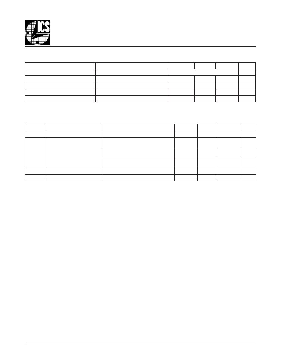
O
UTPUT
D
UTY
C
YCLE
/P
ULSE
W
IDTH
/P
ERIOD
O
UTPUT
R
ISE
/F
ALL
T
IME
3.3V O
UTPUT
L
OAD
AC T
EST
C
IRCUIT
SCOPE
Qx
nQx
LVPECL
2V
-1.3V � 0.165V
Clock
Outputs
20%
80%
80%
20%
t
R
t
F
V
SW I N G
t
PW
t
PERIOD
t
PW
t
PERIOD
odc =
x 100%
Q0
nQ0
V
EE
V
CC
RMS P
HASE
J
ITTER
Phase Noise Mask
Offset Frequency
f
1
f
2
Phase Noise Plot
RMS Jitter = Area Under the Masked Phase Noise Plot
Noise P
o
w
er
843251AG-04
www.icst.com/products/hiperclocks.html
REV. A SEPTEMBER 12, 2005
6
Integrated
Circuit
Systems, Inc.
ICS843251-04
F
EMTO
C
LOCKS
TM C
RYSTAL
-
TO
-
3.3V LVPECL C
LOCK
G
ENERATOR
PRELIMINARY
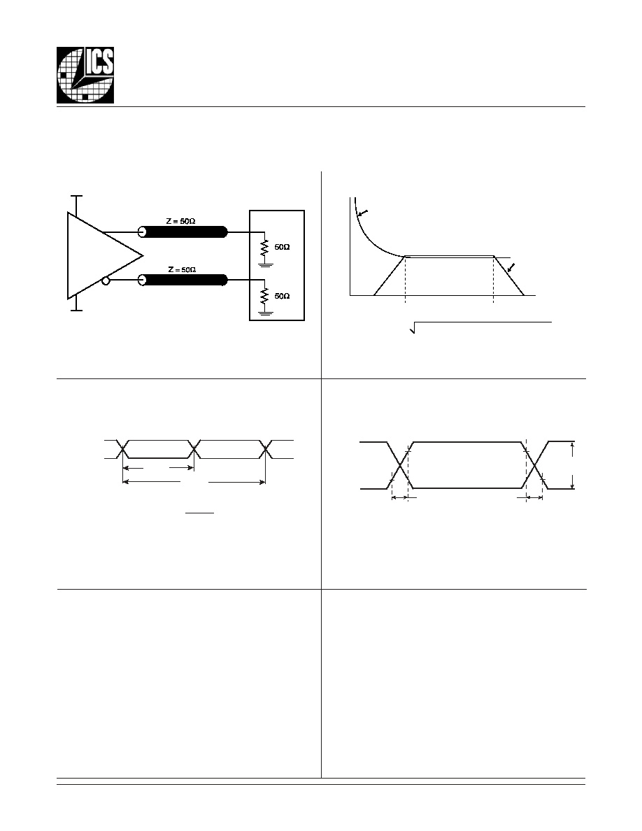
A
PPLICATION
I
NFORMATION
Figure 2. C
RYSTAL
I
NPU
t I
NTERFACE
C
RYSTAL
I
NPUT
I
NTERFACE
The ICS843251-04 has been characterized with 18pF parallel
resonant crystals. The capacitor values, C1 and C2, shown in
Figure 2
below were determined using a 25MHz, 18pF parallel
resonant crystal and were chosen to minimize the ppm error.
The optimum C1 and C2 values can be slightly adjusted for dif-
ferent board layouts.
As in any high speed analog circuitry, the power supply pins
are vulnerable to random noise. The ICS843251-04 provides
separate power supplies to isolate any high switching
noise from the outputs to the internal PLL. V
CC
, and V
CCA
should
b e i n d i v i d u a l l y c o n n e c t e d t o t h e p o w e r s u p p l y
plane through vias, and bypass capacitors should be
used for each pin. To achieve optimum jitter performance,
power supply isolation is required.
Figure 1
illustrates how
a 10
resistor along with a 10F and a .01F bypass
capacitor should be connected to each V
CCA
pin. The 10
resistor can also be replaced by a ferrite bead.
P
OWER
S
UPPLY
F
ILTERING
T
ECHNIQUES
F
IGURE
1. P
OWER
S
UPPLY
F
ILTERING
10
V
CCA
10
F
.01
F
3.3V
.01
F
V
CC
C1
33p
X1
18pF Parallel Crystal
C2
27p
XTAL_OUT
XTAL_IN
843251AG-04
www.icst.com/products/hiperclocks.html
REV. A SEPTEMBER 12, 2005
7
Integrated
Circuit
Systems, Inc.
ICS843251-04
F
EMTO
C
LOCKS
TM C
RYSTAL
-
TO
-
3.3V LVPECL C
LOCK
G
ENERATOR
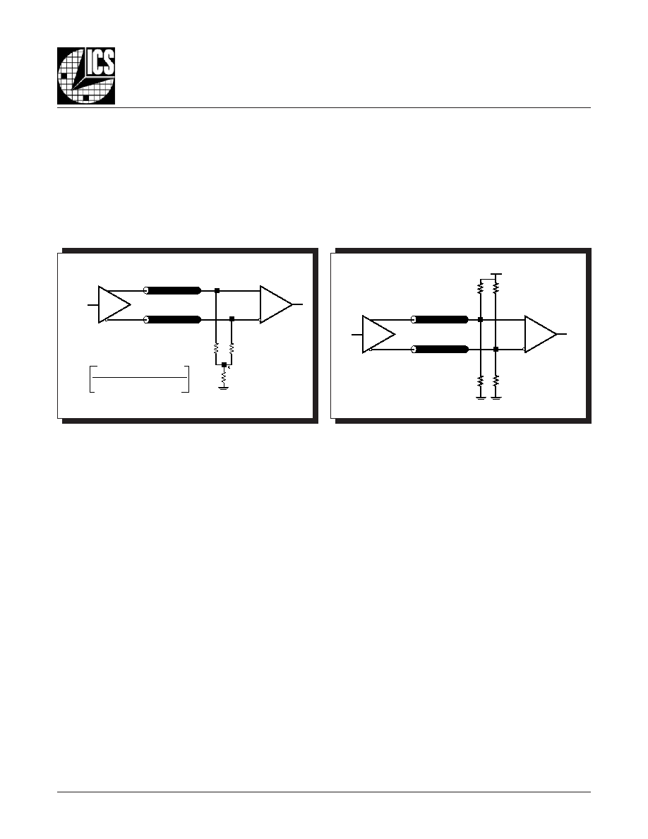
PRELIMINARY
T
ERMINATION
FOR
3.3V LVPECL O
UTPUT
The clock layout topology shown below is a typical termination
for LVPECL outputs. The two different layouts mentioned are
recommended only as guidelines.
FOUT and nFOUT are low impedance follower outputs that
generate ECL/LVPECL compatible outputs. Therefore, terminat-
ing resistors (DC current path to ground) or current sources
must be used for functionality. These outputs are designed to
F
IGURE
3B. LVPECL O
UTPUT
T
ERMINATION
F
IGURE
3A. LVPECL O
UTPUT
T
ERMINATION
drive 50
transmission lines. Matched impedance techniques
should be used to maximize operating frequency and minimize
signal distortion.
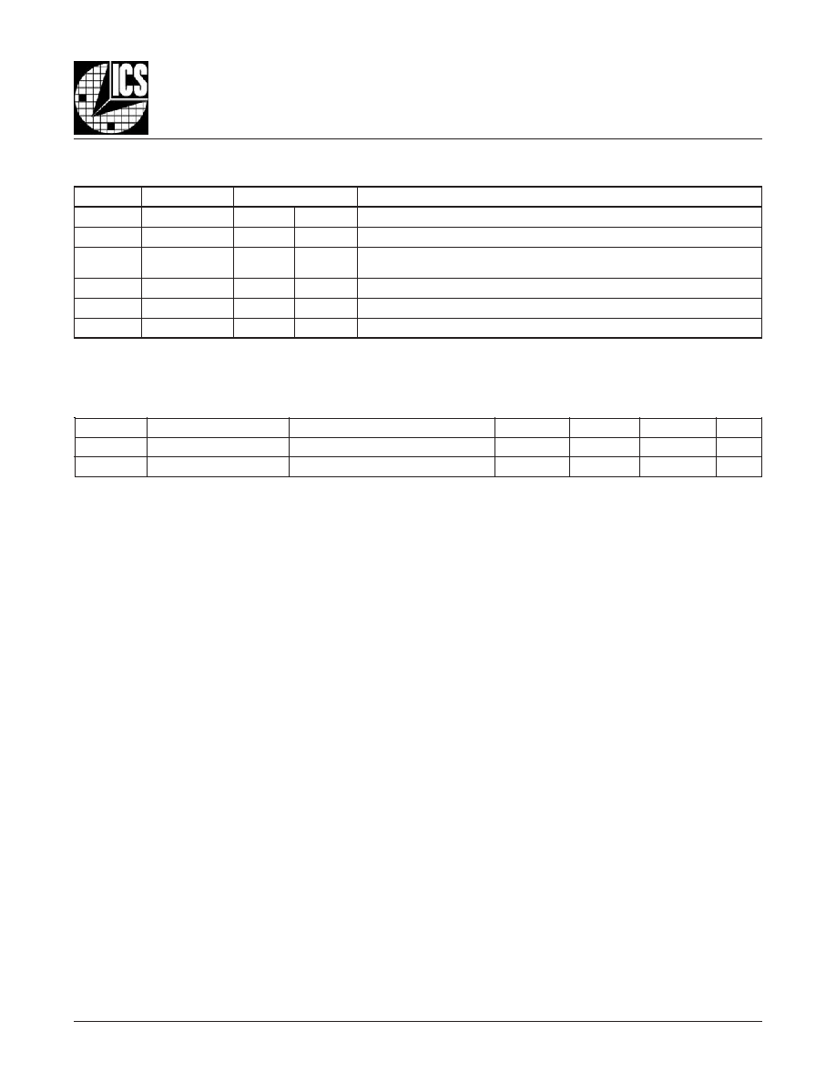
Figures 3A and 3B
show two different layouts
which are recommended only as guidelines. Other suitable clock
layouts may exist and it would be recommended that the board
designers simulate to guarantee compatibility across all printed
circuit and clock component process variations.
V
CC
- 2V
50
50
RTT
Z
o
= 50
Z
o
= 50
FOUT
FIN
RTT =
Z
o
1
((V
OH
+ V
OL
) / (V
CC
� 2)) � 2
3.3V
125
125
84
84
Z
o
= 50
Z
o
= 50
FOUT
FIN

843251AG-04
www.icst.com/products/hiperclocks.html
REV. A SEPTEMBER 12, 2005
8
Integrated
Circuit
Systems, Inc.
ICS843251-04
F
EMTO
C
LOCKS
TM C
RYSTAL
-
TO
-
3.3V LVPECL C
LOCK
G
ENERATOR
PRELIMINARY
R
ELIABILITY
I
NFORMATION
T
RANSISTOR
C
OUNT
The transistor count for ICS843251-04 is: 1891
T
ABLE
6.
JA
VS
. A
IR
F
LOW
T
ABLE
FOR
8 L
EAD
TSSOP
JA
by Velocity (Meters per Second)
0
1
2.5
Multi-Layer PCB, JEDEC Standard Test Boards
101.7�C/W
90.5�C/W
89.8�C/W
843251AG-04
www.icst.com/products/hiperclocks.html
REV. A SEPTEMBER 12, 2005
9
Integrated
Circuit
Systems, Inc.
ICS843251-04
F
EMTO
C
LOCKS
TM C
RYSTAL
-
TO
-
3.3V LVPECL C
LOCK
G
ENERATOR
PRELIMINARY
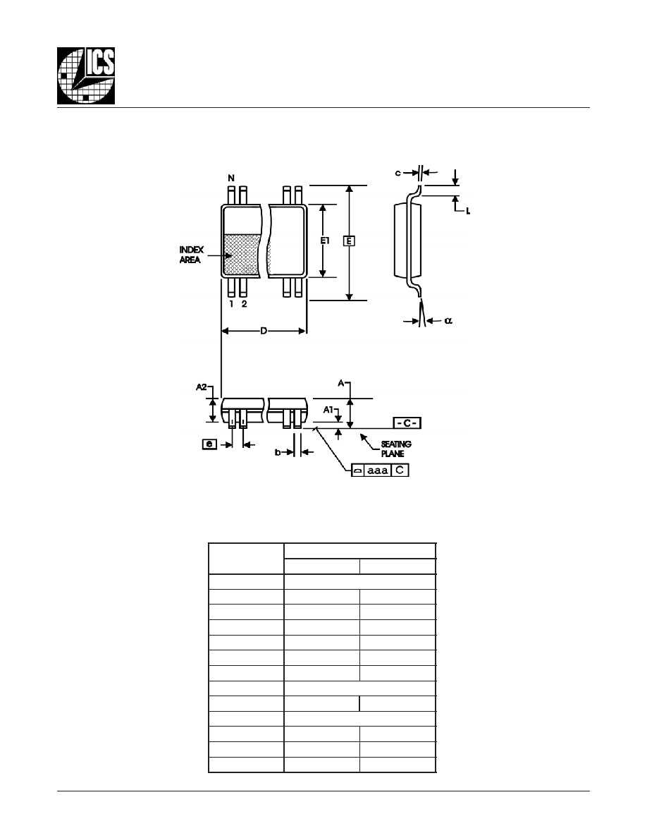
P
ACKAGE
O
UTLINE
- G S
UFFIX
FOR
8 L
EAD
TSSOP
T
ABLE
7. P
ACKAGE
D
IMENSIONS
Reference Document: JEDEC Publication 95, MO-153
L
O
B
M
Y
S
s
r
e
t
e
m
i
l
l
i
M
m
u
m
i
n
i
M
m
u
m
i
x
a
M
N
8
A
-
-
0
2
.
1
1
A
5
0
.
0
5
1
.
0
2
A
0
8
.
0
5
0
.
1
b
9
1
.
0
0
3
.
0
c
9
0
.
0
0
2
.
0
D
0
9
.
2
0
1
.
3
E
C
I
S
A
B
0
4
.
6
1
E
0
3
.
4
0
5
.
4
e
C
I
S
A
B
5
6
.
0
L
5
4
.
0
5
7
.
0
�
0
�
8
a
a
a
-
-
0
1
.
0

843251AG-04
www.icst.com/products/hiperclocks.html
REV. A SEPTEMBER 12, 2005
10
Integrated
Circuit
Systems, Inc.
ICS843251-04
F
EMTO
C
LOCKS
TM C
RYSTAL
-
TO
-
3.3V LVPECL C
LOCK
G
ENERATOR
PRELIMINARY
T
ABLE
8. O
RDERING
I
NFORMATION
While the information presented herein has been checked for both accuracy and reliability, Integrated Circuit Systems, Incorporated (ICS) assumes no responsibility for either its use
or for infringement of any patents or other rights of third parties, which would result from its use. No other circuits, patents, or licenses are implied. This product is intended for use
in normal commercial applications. Any other applications such as those requiring extended temperature range, high reliability, or other extraordinary environmental requirements are
not recommended without additional processing by ICS. ICS reserves the right to change any circuitry or specifications without notice. ICS does not authorize or warrant any ICS
product for use in life support devices or critical medical instruments.
The aforementioned trademarks, HiPerClockS and FemtoClocks are trademarks of Integrated Circuit Systems, Inc. or its subsidiaries in the United States and/or other countries.
r
e
b
m
u
N
r
e
d
r
O
/
t
r
a
P
g
n
i
k
r
a
M
e
g
a
k
c
a
P
g
n
i
g
a
k
c
a
P
g
n
i
p
p
i
h
S
e
r
u
t
a
r
e
p
m
e
T
4
0
-
G
A
1
5
2
3
4
8
S
C
I
4
0
A
1
5
P
O
S
S
T
d
a
e
L
8
e
b
u
t
C
�
0
7
o
t
C
�
0
T
4
0
-
G
A
1
5
2
3
4
8
S
C
I
4
0
A
1
5
P
O
S
S
T
d
a
e
L
8
l
e
e
r
&
e
p
a
t
0
0
5
2
C
�
0
7
o
t
C
�
0
F
L
4
0
-
G
A
1
5
2
3
4
8
S
C
I
L
4
0
A
1
P
O
S
S
T
"
e
e
r
F
-
d
a
e
L
"
d
a
e
L
8
e
b
u
t
C
�
0
7
o
t
C
�
0
T
F
L
4
0
-
G
A
1
5
2
3
4
8
S
C
I
L
4
0
A
1
P
O
S
S
T
"
e
e
r
F
-
d
a
e
L
"
d
a
e
L
8
l
e
e
r
&
e
p
a
t
0
0
5
2
C
�
0
7
o
t
C
�
0
.
t
n
a
il
p
m
o
c
S
H
o
R
e
r
a
d
n
a
n
o
i
t
a
r
u
g
i
f
n
o
c
e
e
r
F
-
b
P
e
h
t
e
r
a
r
e
b
m
u
n
t
r
a
p
e
h
t
o
t
x
i
f
f
u
s
"
F
L
"
n
a
h
t
i
w
d
e
r
e
d
r
o
e
r
a
t
a
h
t
s
t
r
a
P
:
E
T
O
N