Document Outline
- General Description
- Features
- Function Table
- Block Diagram
- Pin Assignment
- Pin Descriptions
- Pin Characteristics
- Absolute Maximum Ratings
- Power Supply 3.3V DC Characteristics
- LVCMOS 3.3V DC Characteristics
- LVPECL 3.3V DC Characteristics
- Power Supply 3.3V/2.5V DC Characteristics
- LVCMOS 3.3V/2.5V DC Characteristics
- LVPECL 3.3V/2.5V DC Characteristics
- Crystal Characteristics
- 3.3V AC Characteristics
- 3.3V/2.5V AC Characteristics
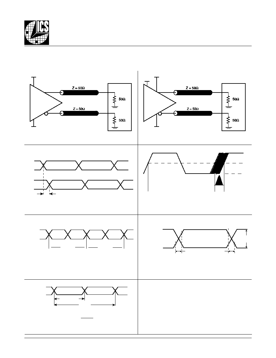
- Parameter Measurement Information
- 3.3V Output Load AC Test Circuit Diagram
- 3.3V/2.5V Output Load AC Test Circuit Diagram
- Output Skew Diagram
- Period Jitter Diagram
- Cycle-to-Cycle Jitter Diagram
- Output Rise/Fall Time Diagram
- odc & tPeriod Diagram
- Applications Information
- Power Supply Filtering Techniques
- Power Supply Filtering Diagram
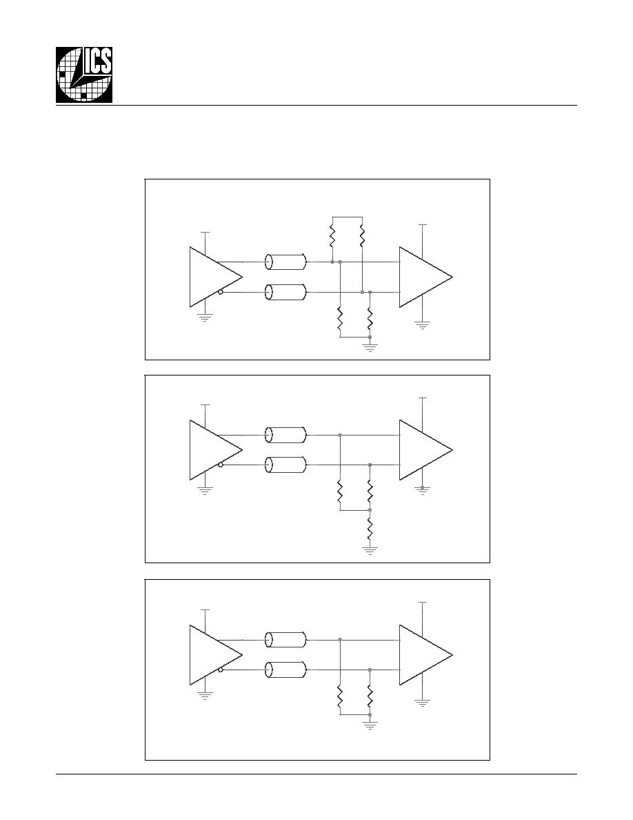
- Terminatin for 3.3V LVPECL Outputs
- LVPECL 3.3V Output Termination Diagrams
- Terminatin for 2.5V LVPECL Outputs
- LVPECL 2.5V Output Termination Diagrams
- Crystal Input Interface
- Crystal Input Interface Diagrams
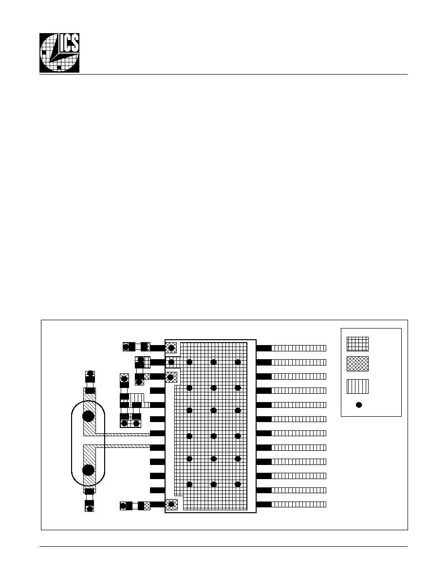
- Schematic Example
- Power & Grounding
- Clock Traces & Termination
- Crystal
- PC Board Layout
- Power Considerations
- Power Dissipation
- Junction Temperature
- Thermal Resistance
- Calculations & Equations
- LVPECL Driver Circuit & Termination Diagram
- Reliability Information
- Transistor Count
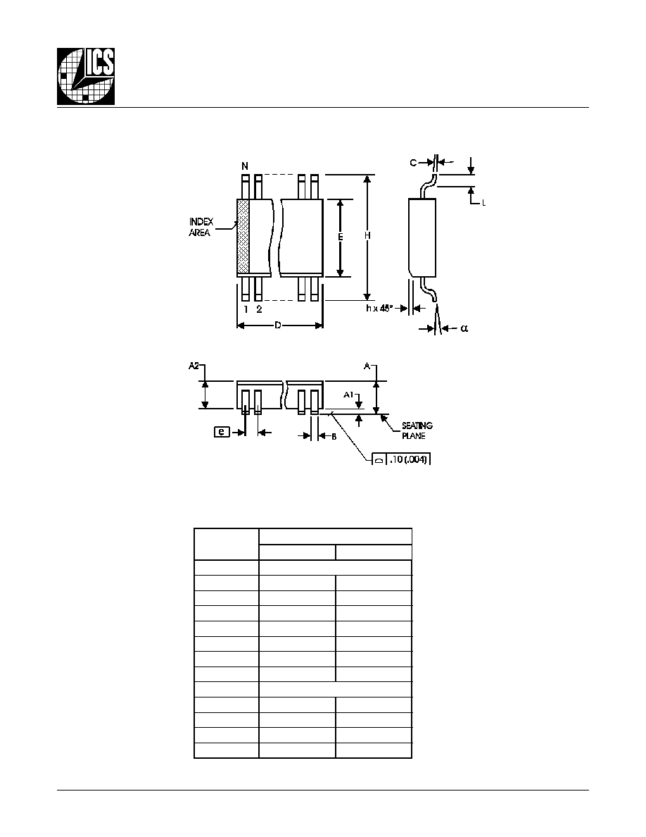
- Package Outline
- Package Dimensions
- Ordering Information
84326AM
www.icst.com/products/hiperclocks.html
REV. A MARCH 10, 2003
1
Integrated
Circuit
Systems, Inc.
ICS84326
C
RYSTAL
-
TO
-3.3V LVPECL
S
ERIAL
A
TTACHED
SCSI C
LOCK
S
YNTHESIZER
/F
ANOUT
B
UFFER
PRELIMINARY
G
ENERAL
D
ESCRIPTION
The ICS84326 is a Crystal-to-3.3V LVPECL Clock
Synthesizer/Fanout Buffer designed for Serial
Attached SCSI applications and is a member of
the HiperClockS family of High Performance Clock
Solutions from ICS. Using a 25MHz crystal, the
6 LVPECL outputs can be set for either 75MHz or 150MHz
using the frequency select pins. The low jitter/low phase noise
characteristics make it an ideal clock source for use in Serial
Attached SCSI applications or for other applications which
require a 75MHz or 150MHz reference clock.
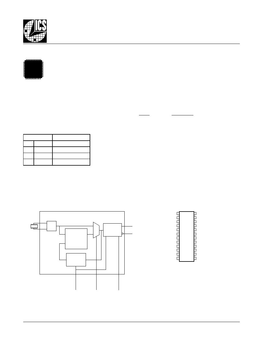
B
LOCK
D
IAGRAM
P
IN
A
SSIGNMENT
F
EATURES
∑
6 LVPECL outputs
∑
Crystal oscillator interface
∑
Output frequency: 75MHz or 150MHz
∑
Crystal input frequency: 25MHz
∑
Cycle-to-cycle jitter: 20ps (typical)
∑
RMS phase jitter at 150MHz, using a 25MHz crystal
(899.8KHz to 20MHz): TBD
∑
Phase noise:
Offset
Noise Power
100Hz ............... TBD
1KHz ............... TBD
10KHz ............... TBD
100KHz ............... TBD
∑
Full 3.3V or 3.3V core, 2.5V supply mode
∑
0∞C to 70∞C ambient operating temperature
∑
Industrial temperature information available upon request
HiPerClockSTM
,&6
Q0:Q5
ICS84326
24-Lead, 300-MIL SOIC
7.5mm x 15.33mm x 2.3mm body package
M Package
Top View
Q0
nQ0
Q1
nQ1
Q2
nQ2
Q3
nQ3
Q4
nQ4
Q5
nQ5
1
2
3
4
5
6
7
8
9
10
11
12
V
CCO
F_SEL
nc
MR
XTAL1
XTAL2
nc
V
CCA
V
CC
PLL_SEL
V
EE
V
CCO
PLL
6
/
Feedback
Divider
OSC
6
/
Output
Divider
0
1
XTAL1
XTAL2
PLL_SEL
MR
F_SEL
nQ0:nQ5
24
23
22
21
20
19
18
17
16
15
14
13
F
UNCTION
T
ABLE
s
t
u
p
n
I
y
c
n
e
u
q
e
r
F
t
u
p
t
u
O
R
M
L
E
S
_
F
T
U
O
_
F
1
X
W
O
L
0
0
z
H
M
5
7
0
1
z
H
M
0
5
1
The Preliminary Information presented herein represents a product in prototyping or pre-production. The noted characteristics are based on initial
product characterization. Integrated Circuit Systems, Incorporated (ICS) reserves the right to change any circuitry or specifications without notice.
84326AM
www.icst.com/products/hiperclocks.html
REV. A MARCH 10, 2003
2
Integrated
Circuit
Systems, Inc.
ICS84326
C
RYSTAL
-
TO
-3.3V LVPECL
S
ERIAL
A
TTACHED
SCSI C
LOCK
S
YNTHESIZER
/F
ANOUT
B
UFFER
PRELIMINARY
T
ABLE
1. P
IN
D
ESCRIPTIONS
T
ABLE
2. P
IN
C
HARACTERISTICS
l
o
b
m
y
S
r
e
t
e
m
a
r
a
P
s
n
o
i
t
i
d
n
o
C
t
s
e
T
m
u
m
i
n
i
M
l
a
c
i
p
y
T
m
u
m
i
x
a
M
s
t
i
n
U
C
N
I
e
c
n
a
t
i
c
a
p
a
C
t
u
p
n
I
4
F
p
R
P
U
L
L
U
P
r
o
t
s
i
s
e
R
p
u
ll
u
P
t
u
p
n
I
1
5
K
R
N
W
O
D
L
L
U
P
r
o
t
s
i
s
e
R
n
w
o
d
ll
u
P
t
u
p
n
I
1
5
K
r
e
b
m
u
N
e
m
a
N
e
p
y
T
n
o
i
t
p
i
r
c
s
e
D
2
,
1
0
Q
n
,
0
Q
t
u
p
t
u
O
.
s
l
e
v
e
l
e
c
a
f
r
e
t
n
i
L
C
E
P
V
L
.
r
i
a
p
t
u
p
t
u
o
l
a
i
t
n
e
r
e
f
f
i
D
4
,
3
1
Q
n
,
1
Q
t
u
p
t
u
O
.
s
l
e
v
e
l
e
c
a
f
r
e
t
n
i
L
C
E
P
V
L
.
r
i
a
p
t
u
p
t
u
o
l
a
i
t
n
e
r
e
f
f
i
D
6
,
5
2
Q
n
,
2
Q
t
u
p
t
u
O
.
s
l
e
v
e
l
e
c
a
f
r
e
t
n
i
L
C
E
P
V
L
.
r
i
a
p
t
u
p
t
u
o
l
a
i
t
n
e
r
e
f
f
i
D
8
,
7
3
Q
n
,
3
Q
t
u
p
t
u
O
.
s
l
e
v
e
l
e
c
a
f
r
e
t
n
i
L
C
E
P
V
L
.
r
i
a
p
t
u
p
t
u
o
l
a
i
t
n
e
r
e
f
f
i
D
0
1
,
9
4
Q
n
,
4
Q
t
u
p
t
u
O
.
s
l
e
v
e
l
e
c
a
f
r
e
t
n
i
L
C
E
P
V
L
.
r
i
a
p
t
u
p
t
u
o
l
a
i
t
n
e
r
e
f
f
i
D
2
1
,
1
1
5
Q
n
,
5
Q
t
u
p
t
u
O
.
s
l
e
v
e
l
e
c
a
f
r
e
t
n
i
L
C
E
P
V
L
.
r
i
a
p
t
u
p
t
u
o
l
a
i
t
n
e
r
e
f
f
i
D
4
2
,
3
1
V
O
C
C
r
e
w
o
P
.
s
n
i
p
y
l
p
p
u
s
t
u
p
t
u
O
6
1
V
C
C
r
e
w
o
P
.
n
i
p
y
l
p
p
u
s
e
r
o
C
4
1
V
E
E
.
n
i
p
y
l
p
p
u
s
e
v
i
t
a
g
e
N
5
1
L
E
S
_
L
L
P
t
u
p
n
I
p
u
ll
u
P
e
h
t
o
t
t
u
p
n
i
e
h
t
s
a
s
t
u
p
n
i
l
a
t
s
y
r
c
d
n
a
L
L
P
e
h
t
n
e
e
w
t
e
b
s
t
c
e
l
e
S
.
2
L
A
T
X
,
1
L
A
T
X
s
t
c
e
l
e
s
,
W
O
L
n
e
h
W
.
L
L
P
s
t
c
e
l
e
s
,
H
G
I
H
n
e
h
W
.
s
r
e
d
i
v
i
d
.
s
l
e
v
e
l
e
c
a
f
r
e
t
n
i
L
T
T
V
L
/
S
O
M
C
V
L
7
1
V
A
C
C
r
e
w
o
P
.
n
i
p
y
l
p
p
u
s
g
o
l
a
n
A
2
2
,
8
1
c
n
d
e
s
u
n
U
.
t
c
e
n
n
o
c
o
N
0
2
,
9
1
1
L
A
T
X
,
2
L
A
T
X
t
u
p
n
I
.
t
u
p
t
u
o
e
h
t
s
i
2
L
A
T
X
.
t
u
p
n
i
e
h
t
s
i
1
L
A
T
X
.
e
c
a
f
r
e
t
n
i
r
o
t
a
ll
i
c
s
o
l
a
t
s
y
r
C
1
2
R
M
t
u
p
n
I
n
w
o
d
ll
u
P
s
r
e
d
i
v
i
d
l
a
n
r
e
t
n
i
e
h
t
,
H
G
I
H
c
i
g
o
l
n
e
h
W
.
t
e
s
e
R
r
e
t
s
a
M
h
g
i
H
e
v
i
t
c
A
d
e
t
r
e
v
n
i
e
h
t
d
n
a
,
w
o
l
o
g
o
t
x
Q
s
t
u
p
t
u
o
e
u
r
t
e
h
t
g
n
i
s
u
a
c
t
e
s
e
r
e
r
a
d
n
a
s
r
e
d
i
v
i
d
l
a
n
r
e
t
n
i
e
h
t
,
W
O
L
c
i
g
o
l
n
e
h
W
.
h
g
i
h
o
g
o
t
x
Q
n
s
t
u
p
t
u
o
.
s
l
e
v
e
l
e
c
a
f
r
e
t
n
i
L
T
T
V
L
/
S
O
M
C
V
L
.
d
e
l
b
a
n
e
e
r
a
s
t
u
p
t
u
o
e
h
t
3
2
L
E
S
_
F
t
u
p
n
I
p
u
ll
u
P
.
s
l
e
v
e
l
e
c
a
f
r
e
t
n
i
L
T
T
V
L
/
S
O
M
C
V
L
.
n
i
p
t
c
e
l
e
s
y
c
n
e
u
q
e
r
f
t
u
p
t
u
O
:
E
T
O
N
p
u
ll
u
P
d
n
a
n
w
o
d
ll
u
P
.
s
e
u
l
a
v
l
a
c
i
p
y
t
r
o
f
,
s
c
i
t
s
i
r
e
t
c
a
r
a
h
C
n
i
P
,
2
e
l
b
a
T
e
e
S
.
s
r
o
t
s
i
s
e
r
t
u
p
n
i
l
a
n
r
e
t
n
i
o
t
r
e
f
e
r

84326AM
www.icst.com/products/hiperclocks.html
REV. A MARCH 10, 2003
3
Integrated
Circuit
Systems, Inc.
ICS84326
C
RYSTAL
-
TO
-3.3V LVPECL
S
ERIAL
A
TTACHED
SCSI C
LOCK
S
YNTHESIZER
/F
ANOUT
B
UFFER
PRELIMINARY
T
ABLE
3B. LVCMOS / LVTTL DC C
HARACTERISTICS
,
V
CC
= V
CCA
= V
CCO
= 3.3V±5%, T
A
= 0∞C
TO
70∞C
l
o
b
m
y
S
r
e
t
e
m
a
r
a
P
s
n
o
i
t
i
d
n
o
C
t
s
e
T
m
u
m
i
n
i
M
l
a
c
i
p
y
T
m
u
m
i
x
a
M
s
t
i
n
U
V
C
C
e
g
a
t
l
o
V
y
l
p
p
u
S
e
r
o
C
5
3
1
.
3
3
.
3
5
6
4
.
3
V
V
A
C
C
e
g
a
t
l
o
V
y
l
p
p
u
S
g
o
l
a
n
A
5
3
1
.
3
3
.
3
5
6
4
.
3
V
V
O
C
C
e
g
a
t
l
o
V
y
l
p
p
u
S
t
u
p
t
u
O
5
3
1
.
3
3
.
3
5
6
4
.
3
V
I
E
E
t
n
e
r
r
u
C
y
l
p
p
u
S
r
e
w
o
P
0
4
1
A
m
I
A
C
C
t
n
e
r
r
u
C
y
l
p
p
u
S
g
o
l
a
n
A
0
2
A
m
l
o
b
m
y
S
r
e
t
e
m
a
r
a
P
s
n
o
i
t
i
d
n
o
C
t
s
e
T
m
u
m
i
n
i
M
l
a
c
i
p
y
T
m
u
m
i
x
a
M
s
t
i
n
U
V
H
I
e
g
a
t
l
o
V
h
g
i
H
t
u
p
n
I
,
R
M
,
L
E
S
_
L
L
P
L
E
S
_
F
2
V
C
C
3
.
0
+
V
V
L
I
e
g
a
t
l
o
V
w
o
L
t
u
p
n
I
,
R
M
,
L
E
S
_
L
L
P
L
E
S
_
F
3
.
0
-
8
.
0
V
I
H
I
t
n
e
r
r
u
C
h
g
i
H
t
u
p
n
I
R
M
V
C
C
V
=
N
I
V
5
6
4
.
3
=
0
5
1
A
µ
L
E
S
_
F
,
L
E
S
_
L
L
P
V
C
C
V
=
N
I
V
5
6
4
.
3
=
5
A
µ
I
L
I
t
n
e
r
r
u
C
w
o
L
t
u
p
n
I
R
M
V
C
C
V
,
V
5
6
4
.
3
=
N
I
V
0
=
5
-
A
µ
L
E
S
_
F
,
L
E
S
_
L
L
P
V
C
C
V
,
V
5
6
4
.
3
=
N
I
V
0
=
0
5
1
-
A
µ
T
ABLE
3C. LVPECL DC C
HARACTERISTICS
,
V
CC
= V
CCA
= V
CCO
= 3.3V±5%, T
A
= 0∞C
TO
70∞C
A
BSOLUTE
M
AXIMUM
R
ATINGS
Supply Voltage, V
CC
4.6V
Inputs, V
I
-0.5V to V
CC
+ 0.5 V
Outputs, V
O
-0.5V to V
CCO
+ 0.5V
Package Thermal Impedance,
JA
50∞C/W (0 lfpm)
Storage Temperature, T
STG
-65∞C to 150∞C
NOTE: Stresses beyond those listed under Absolute
Maximum Ratings may cause permanent damage to the
device. These ratings are stress specifications only. Functional
operation of product at these conditions or any conditions be-
yond those listed in the
DC Characteristics or AC Character-
istics is not implied. Exposure to absolute maximum rating
conditions for extended periods may affect product reliability.
T
ABLE
3A. P
OWER
S
UPPLY
DC C
HARACTERISTICS
,
V
CC
= V
CCA
= V
CCO
= 3.3V±5%, T
A
= 0∞C
TO
70∞C
l
o
b
m
y
S
r
e
t
e
m
a
r
a
P
s
n
o
i
t
i
d
n
o
C
t
s
e
T
m
u
m
i
n
i
M
l
a
c
i
p
y
T
m
u
m
i
x
a
M
s
t
i
n
U
V
H
O
1
E
T
O
N
;
e
g
a
t
l
o
V
h
g
i
H
t
u
p
t
u
O
V
O
C
C
4
.
1
-
V
O
C
C
0
.
1
-
V
V
L
O
1
E
T
O
N
;
e
g
a
t
l
o
V
w
o
L
t
u
p
t
u
O
V
O
C
C
0
.
2
-
V
O
C
C
7
.
1
-
V
V
G
N
I
W
S
g
n
i
w
S
e
g
a
t
l
o
V
t
u
p
t
u
O
k
a
e
P
-
o
t
-
k
a
e
P
6
.
0
0
.
1
V
0
5
h
t
i
w
d
e
t
a
n
i
m
r
e
t
s
t
u
p
t
u
O
:
1
E
T
O
N
V
o
t
O
C
C
.
V
2
-

84326AM
www.icst.com/products/hiperclocks.html
REV. A MARCH 10, 2003
4
Integrated
Circuit
Systems, Inc.
ICS84326
C
RYSTAL
-
TO
-3.3V LVPECL
S
ERIAL
A
TTACHED
SCSI C
LOCK
S
YNTHESIZER
/F
ANOUT
B
UFFER
PRELIMINARY
T
ABLE
4. C
RYSTAL
C
HARACTERISTICS
r
e
t
e
m
a
r
a
P
s
n
o
i
t
i
d
n
o
C
t
s
e
T
m
u
m
i
n
i
M
l
a
c
i
p
y
T
m
u
m
i
x
a
M
s
t
i
n
U
n
o
i
t
a
ll
i
c
s
O
f
o
e
d
o
M
l
a
t
n
e
m
a
d
n
u
F
y
c
n
e
u
q
e
r
F
5
2
z
H
M
)
R
S
E
(
e
c
n
a
t
s
i
s
e
R
s
e
i
r
e
S
t
n
e
l
a
v
i
u
q
E
0
7
e
c
n
a
t
i
c
a
p
a
C
t
n
u
h
S
7
F
p
.
l
a
t
s
y
r
c
t
n
a
n
o
s
e
r
l
e
ll
a
r
a
p
f
p
8
1
n
a
g
n
i
s
u
d
e
z
i
r
e
t
c
a
r
a
h
C
:
E
T
O
N
T
ABLE
3E. LVCMOS / LVTTL DC C
HARACTERISTICS
,
V
CC
= V
CCA
= 3.3V±5%, V
CCO
= 2.5V±5%, T
A
= 0∞C
TO
70∞C
l
o
b
m
y
S
r
e
t
e
m
a
r
a
P
s
n
o
i
t
i
d
n
o
C
t
s
e
T
m
u
m
i
n
i
M
l
a
c
i
p
y
T
m
u
m
i
x
a
M
s
t
i
n
U
V
C
C
e
g
a
t
l
o
V
y
l
p
p
u
S
e
r
o
C
5
3
1
.
3
3
.
3
5
6
4
.
3
V
V
A
C
C
e
g
a
t
l
o
V
y
l
p
p
u
S
g
o
l
a
n
A
5
3
1
.
3
3
.
3
5
6
4
.
3
V
V
O
C
C
e
g
a
t
l
o
V
y
l
p
p
u
S
t
u
p
t
u
O
5
7
3
.
2
5
.
2
5
2
6
.
2
V
I
E
E
t
n
e
r
r
u
C
y
l
p
p
u
S
r
e
w
o
P
0
4
1
A
m
I
A
C
C
t
n
e
r
r
u
C
y
l
p
p
u
S
g
o
l
a
n
A
0
2
A
m
l
o
b
m
y
S
r
e
t
e
m
a
r
a
P
s
n
o
i
t
i
d
n
o
C
t
s
e
T
m
u
m
i
n
i
M
l
a
c
i
p
y
T
m
u
m
i
x
a
M
s
t
i
n
U
V
H
I
e
g
a
t
l
o
V
h
g
i
H
t
u
p
n
I
,
R
M
,
L
E
S
_
L
L
P
L
E
S
_
F
2
V
C
C
3
.
0
+
V
V
L
I
e
g
a
t
l
o
V
w
o
L
t
u
p
n
I
,
R
M
,
L
E
S
_
L
L
P
L
E
S
_
F
3
.
0
-
8
.
0
V
I
H
I
t
n
e
r
r
u
C
h
g
i
H
t
u
p
n
I
R
M
V
C
C
V
=
N
I
V
5
6
4
.
3
=
0
5
1
A
µ
L
E
S
_
F
,
L
E
S
_
L
L
P
V
C
C
V
=
N
I
V
5
6
4
.
3
=
5
A
µ
I
L
I
t
n
e
r
r
u
C
w
o
L
t
u
p
n
I
R
M
V
C
C
V
,
V
5
6
4
.
3
=
N
I
V
0
=
5
-
A
µ
L
E
S
_
F
,
L
E
S
_
L
L
P
V
C
C
V
,
V
5
6
4
.
3
=
N
I
V
0
=
0
5
1
-
A
µ
T
ABLE
3F. LVPECL DC C
HARACTERISTICS
,
V
CC
= V
CCA
= 3.3V±5%, V
CCO
= 2.5V±5%, T
A
= 0∞C
TO
70∞C
T
ABLE
3D. P
OWER
S
UPPLY
DC C
HARACTERISTICS
,
V
CC
= V
CCA
= 3.3V±5%, V
CCO
= 2.5V±5%, T
A
= 0∞C
TO
70∞C
l
o
b
m
y
S
r
e
t
e
m
a
r
a
P
s
n
o
i
t
i
d
n
o
C
t
s
e
T
m
u
m
i
n
i
M
l
a
c
i
p
y
T
m
u
m
i
x
a
M
s
t
i
n
U
V
H
O
1
E
T
O
N
;
e
g
a
t
l
o
V
h
g
i
H
t
u
p
t
u
O
V
O
C
C
4
.
1
-
V
O
C
C
0
.
1
-
V
V
L
O
1
E
T
O
N
;
e
g
a
t
l
o
V
w
o
L
t
u
p
t
u
O
V
O
C
C
0
.
2
-
V
O
C
C
7
.
1
-
V
V
G
N
I
W
S
g
n
i
w
S
e
g
a
t
l
o
V
t
u
p
t
u
O
k
a
e
P
-
o
t
-
k
a
e
P
6
.
0
0
.
1
V
0
5
h
t
i
w
d
e
t
a
n
i
m
r
e
t
s
t
u
p
t
u
O
:
1
E
T
O
N
V
o
t
O
C
C
.
V
2
-

84326AM
www.icst.com/products/hiperclocks.html
REV. A MARCH 10, 2003
5
Integrated
Circuit
Systems, Inc.
ICS84326
C
RYSTAL
-
TO
-3.3V LVPECL
S
ERIAL
A
TTACHED
SCSI C
LOCK
S
YNTHESIZER
/F
ANOUT
B
UFFER
PRELIMINARY
l
o
b
m
y
S
r
e
t
e
m
a
r
a
P
s
n
o
i
t
i
d
n
o
C
t
s
e
T
m
u
m
i
n
i
M
l
a
c
i
p
y
T
m
u
m
i
x
a
M
s
t
i
n
U
F
T
U
O
y
c
n
e
u
q
e
r
F
t
u
p
t
u
O
5
7
0
5
1
z
H
M
t
)
c
c
(
t
ij
2
E
T
O
N
;
r
e
t
t
i
J
e
l
c
y
C
-
o
t
-
e
l
c
y
C
0
2
s
p
t
)
r
e
p
(
t
ij
S
M
R
,
r
e
t
t
i
J
d
o
i
r
e
P
D
B
T
s
p
t
)
o
(
k
s
2
,
1
E
T
O
N
;
w
e
k
S
t
u
p
t
u
O
0
5
s
p
t
R
/ t
F
e
m
i
T
ll
a
F
/
e
s
i
R
t
u
p
t
u
O
%
0
8
o
t
%
0
2
0
0
2
0
0
7
s
p
c
d
o
e
l
c
y
C
y
t
u
D
t
u
p
t
u
O
0
5
%
t
K
C
O
L
e
m
i
T
k
c
o
L
L
L
P
1
s
m
.
n
o
i
t
c
e
s
n
o
i
t
a
m
r
o
f
n
I
t
n
e
m
e
r
u
s
a
e
M
r
e
t
e
m
a
r
a
P
e
e
S
.
s
n
o
i
t
i
d
n
o
c
d
a
o
l
l
a
u
q
e
h
t
i
w
d
n
a
e
g
a
t
l
o
v
y
l
p
p
u
s
e
m
a
s
e
h
t
t
a
s
t
u
p
t
u
o
n
e
e
w
t
e
b
w
e
k
s
s
a
d
e
n
i
f
e
D
:
1
E
T
O
N
.
s
t
n
i
o
p
g
n
i
s
s
o
r
c
l
a
i
t
n
e
r
e
f
f
i
d
t
u
p
t
u
o
e
h
t
t
a
d
e
r
u
s
a
e
M
.
5
6
d
r
a
d
n
a
t
S
C
E
D
E
J
h
t
i
w
e
c
n
a
d
r
o
c
c
a
n
i
d
e
n
i
f
e
d
s
i
r
e
t
e
m
a
r
a
p
s
i
h
T
:
2
E
T
O
N
T
ABLE
5A. AC C
HARACTERISTICS
,
V
CC
= V
CCA
= V
CCO
= 3.3V±5%, T
A
= 0∞C
TO
70∞C
l
o
b
m
y
S
r
e
t
e
m
a
r
a
P
s
n
o
i
t
i
d
n
o
C
t
s
e
T
m
u
m
i
n
i
M
l
a
c
i
p
y
T
m
u
m
i
x
a
M
s
t
i
n
U
F
T
U
O
y
c
n
e
u
q
e
r
F
t
u
p
t
u
O
5
7
0
5
1
z
H
M
t
)
c
c
(
t
ij
2
E
T
O
N
;
r
e
t
t
i
J
e
l
c
y
C
-
o
t
-
e
l
c
y
C
0
2
s
p
t
)
r
e
p
(
t
ij
S
M
R
,
r
e
t
t
i
J
d
o
i
r
e
P
D
B
T
s
p
t
)
o
(
k
s
2
,
1
E
T
O
N
;
w
e
k
S
t
u
p
t
u
O
5
3
s
p
t
R
t
/
F
e
m
i
T
ll
a
F
/
e
s
i
R
t
u
p
t
u
O
%
0
8
o
t
%
0
2
0
0
2
0
0
7
s
p
c
d
o
e
l
c
y
C
y
t
u
D
t
u
p
t
u
O
0
5
%
t
K
C
O
L
e
m
i
T
k
c
o
L
L
L
P
1
s
m
.
n
o
i
t
c
e
s
n
o
i
t
a
m
r
o
f
n
I
t
n
e
m
e
r
u
s
a
e
M
r
e
t
e
m
a
r
a
P
e
e
S
.
s
n
o
i
t
i
d
n
o
c
d
a
o
l
l
a
u
q
e
h
t
i
w
d
n
a
e
g
a
t
l
o
v
y
l
p
p
u
s
e
m
a
s
e
h
t
t
a
s
t
u
p
t
u
o
n
e
e
w
t
e
b
w
e
k
s
s
a
d
e
n
i
f
e
D
:
1
E
T
O
N
.
s
t
n
i
o
p
g
n
i
s
s
o
r
c
l
a
i
t
n
e
r
e
f
f
i
d
t
u
p
t
u
o
e
h
t
t
a
d
e
r
u
s
a
e
M
.
5
6
d
r
a
d
n
a
t
S
C
E
D
E
J
h
t
i
w
e
c
n
a
d
r
o
c
c
a
n
i
d
e
n
i
f
e
d
s
i
r
e
t
e
m
a
r
a
p
s
i
h
T
:
2
E
T
O
N
T
ABLE
5B. AC C
HARACTERISTICS
,
V
CC
= V
CCA
= 3.3V±5%, V
CCO
= 2.5V±5%, T
A
= 0∞C
TO
70∞C
84326AM
www.icst.com/products/hiperclocks.html
REV. A MARCH 10, 2003
6
Integrated
Circuit
Systems, Inc.
ICS84326
C
RYSTAL
-
TO
-3.3V LVPECL
S
ERIAL
A
TTACHED
SCSI C
LOCK
S
YNTHESIZER
/F
ANOUT
B
UFFER
PRELIMINARY
P
ARAMETER
M
EASUREMENT
I
NFORMATION
3.3V/2.5V O
UTPUT
L
OAD
AC T
EST
C
IRCUIT
odc & t
P
ERIOD
C
YCLE
-
TO
-C
YCLE
J
ITTER
O
UTPUT
R
ISE
/F
ALL
T
IME
V
OH
V
REF
V
OL
Mean Period
(First edge after trigger)
Reference Point
(Trigger Edge)
1
contains 68.26% of all measurements
2
contains 95.4% of all measurements
3
contains 99.73% of all measurements
4
contains 99.99366% of all measurements
6
contains (100-1.973x10
-7
)% of all measurements
Histogram
Clock Outputs
20%
80%
80%
20%
t
R
t
F
V
SW I N G
Pulse Width
t
PERIOD
t
PW
t
PERIOD
odc =
nQ0:nQ5
Q0:Q5
nQ0:nQ5
Q0:Q5
tsk(o)
nQx
Qx
nQy
Qy
3.3V O
UTPUT
L
OAD
AC T
EST
C
IRCUIT
SCOPE
Qx
nQx
LVPECL
V
CC
, V
CCA
, V
CCO
= 2V
V
EE
= -1.3V ± 0.165V
P
ERIOD
J
ITTER
O
UTPUT
S
KEW
SCOPE
Qx
nQx
LVPECL
V
CCO
V
EE
= -0.5V ± 0.165V
2V
2.8V
V
CC
,
V
CCA
t
jit(cc) =
t
cycle n ≠
t
cycle n+1
1000 Cycles
t
cycle n
t
cycle n+1
84326AM
www.icst.com/products/hiperclocks.html
REV. A MARCH 10, 2003
7
Integrated
Circuit
Systems, Inc.
ICS84326
C
RYSTAL
-
TO
-3.3V LVPECL
S
ERIAL
A
TTACHED
SCSI C
LOCK
S
YNTHESIZER
/F
ANOUT
B
UFFER
PRELIMINARY
As in any high speed analog circuitry, the power supply pins
are vulnerable to random noise. The ICS84326 provides sepa-
r a t e p o w e r s u p p l i e s t o i s o l a t e a n y h i g h s w i t c h i n g
noise from the outputs to the internal PLL. V
CC
, V
CCA
and V
CCO
should be individually connected to the power supply plane
through vias, and bypass capacitors should be used for each
pin. To achieve optimum jitter performance, power supply iso-
lation is required.
Figure 1 illustrates how a 20
resistor along
with a 10
µ
F and a .01
µ
F bypass capacitor should be con-
nected to each V
CCA
pin.
P
OWER
S
UPPLY
F
ILTERING
T
ECHNIQUES
F
IGURE
1. P
OWER
S
UPPLY
F
ILTERING
20
V
CCA
10
µ
F
.01
µ
F
3.3V
.01
µ
F
V
CC
A
PPLICATION
I
NFORMATION
T
ERMINATION
FOR
3.3V LVPECL O
UTPUTS
The clock layout topology shown below is a typical termina-
tion for 3.3V LVPECL outputs. The two different layouts
mentioned are recommended only as guidelines.
FOUT and nFOUT are low impedance follower outputs that
generate ECL/LVPECL compatible outputs. Therefore, termi-
nating resistors (DC current path to ground) or current
sources must be used for functionality. These outputs are
F
IGURE
2B. LVPECL O
UTPUT
T
ERMINATION
3.3V
F
OUT
F
IN
5
2 Z
o
Z
o
5
2
Z
o
3
2
Z
o
3
2
Z
o
= 50
Z
o
= 50
F
IGURE
2A. LVPECL O
UTPUT
T
ERMINATION
RTT =
1
(V
OH
+ V
OL
/ V
CC
≠2) ≠2
Z
o
Z
o
= 50
Z
o
= 50
50
50
RTT
V
CC
- 2V
F
IN
F
OUT
designed to drive 50
transmission lines. Matched impedance
t e c h n i q u e s s h o u l d b e u s e d t o m a x i m i z e o p e r a t i n g
frequency and minimize signal distortion.
Figures 2A and 2B
show two different layouts which are recommended only
as guidelines. Other suitable clock layouts may exist and it
would be recommended that the board designers simulate to
guarantee compatibility across all printed circuit and clock
component process variations.
84326AM
www.icst.com/products/hiperclocks.html
REV. A MARCH 10, 2003
8
Integrated
Circuit
Systems, Inc.
ICS84326
C
RYSTAL
-
TO
-3.3V LVPECL
S
ERIAL
A
TTACHED
SCSI C
LOCK
S
YNTHESIZER
/F
ANOUT
B
UFFER
PRELIMINARY
2.5V
Zo = 50 Ohm
R3
18
+
-
Zo = 50 Ohm
2.5V
R2
50
R1
50
2,5V LVPECL
Driver
R3
250
+
-
2.5V
2,5V LVPECL
Driver
2.5V
Zo = 50 Ohm
R4
62.5
R2
62.5
2.5V
Zo = 50 Ohm
R1
250
2.5V
R1
50
R2
50
+
-
Zo = 50 Ohm
2.5V
2,5V LVPECL
Driver
Zo = 50 Ohm
T
ERMINATION
FOR
2.5V LVPECL O
UTPUT
Figure 3A and Figure 3B show examples of termination for 2.5V
LVPECL driver. These terminations are equivalent to terminat-
ing 50
to V
CC
- 2V. For V
CC
= 2.5V, the V
CC
- 2V is very close to
ground level. The R3 in Figure 3B can be eliminated and the
termination is shown in
Figure 3C.
F
IGURE
3A. 2.5V LVPECL D
RIVER
T
ERMINATION
E
XAMPLE
F
IGURE
3B. 2.5V LVPECL D
RIVER
T
ERMINATION
E
XAMPLE
F
IGURE
3C. 2.5V LVPECL T
ERMINATION
E
XAMPLE

84326AM
www.icst.com/products/hiperclocks.html
REV. A MARCH 10, 2003
9
Integrated
Circuit
Systems, Inc.
ICS84326
C
RYSTAL
-
TO
-3.3V LVPECL
S
ERIAL
A
TTACHED
SCSI C
LOCK
S
YNTHESIZER
/F
ANOUT
B
UFFER
PRELIMINARY
F
IGURE
5A. ICS84326 S
CHEMATIC
E
XAMPLE
C
RYSTAL
I
NPUT
I
NTERFACE
The ICS84326 has been characterized with 18pF parallel
resonant crystals. The capacitor values, C1 and C2, shown
in
Figure 4 below were determined using a 25MHz, 18pF
Figure 4. C
RYSTAL
I
NPU
t I
NTERFACE
C2
22pF
C1
18pF
25MHz X1
ICS84326
19
20
XTAL2
XTAL1
parallel resonant crystal and were chosen to minimize the
ppm error. The optimum C1 and C2 values can be slightly
adjusted for different board layouts.
S
CHEMATIC
E
XAMPLE
Figure 5A shows a schematic example of using an ICS84326. In
this example, the input is a 25MHz parallel resonant crystal with
load capacitor CL=18pF. The frequency fine tuning capacitors C1
and C2 is 22pF and 18pF respectively. This example also shows
logic control input handling. The configuration is set at F_SEL=0,
therefore, the output frequency is 150MHz. It is recommended to
have one decouple capacitor per power pin. Each decoupling ca-
pacitor should be located as close as possible to the power pin.
The low pass filter R7, C11 and C16 for clean analog supply should
also be located as close to the V
CCA
pin as possible.
X1
25MHz,18pF
C5
0.1u
R6
1K
VCCA
R2
50
VCC
+
-
R5
1K
VCC
R3
50
VCC=3.3V
U1
ICS84326
1
2
3
4
5
6
7
8
9
10
11
12
13
14
15
16
17
18
19
20
21
22
23
24
Q0
nQ0
Q1
nQ1
Q2
nQ2
Q3
nQ3
Q4
nQ4
Q5
nQ5
VCCO
VEE
PLL_SEL
VCC
VCCA
nc
XTAL2
XTAL1
MR
nc
F_SEL
VCCO
(U1,24)
C6
0.1u
C 16
10u
VCC
(U1,13)
C2
18p
VCC
R7
24
R1
50
C11
0.1u
Zo = 50
Zo = 50
R4
1K
(U 1,16)
C3
0.1u
C1
22p
84326AM
www.icst.com/products/hiperclocks.html
REV. A MARCH 10, 2003
10
Integrated
Circuit
Systems, Inc.
ICS84326
C
RYSTAL
-
TO
-3.3V LVPECL
S
ERIAL
A
TTACHED
SCSI C
LOCK
S
YNTHESIZER
/F
ANOUT
B
UFFER
PRELIMINARY
ICS84326
R7
VIA
C1
VCC
GND
C11
C2
C16
U1
C5
Pin1
X1
C6
50 Ohm Traces
C3
Signals
F
IGURE
5B. ICS84326 P.C. B
OARD
L
AYOUT
E
XAMPLE
The following component footprints are used in this layout
example:
All the resistors and capacitors are size 0603.
P
OWER
AND
G
ROUNDING
Place the decoupling capacitors C5, C6 and C3, as close as
possible to the power pins. If space allows, placement of the
decoupling capacitor on the component side is preferred. This
can reduce unwanted inductance between the decoupling ca-
pacitor and the power pin caused by the via.
Maximize the power and ground pad sizes and number of vias
capacitors. This can reduce the inductance between the power
and ground planes and the component power and ground pins.
The RC filter consisting of R7, C11, and C16 should be placed
as close to the V
CCA
pin as possible.
C
LOCK
T
RACES
AND
T
ERMINATION
Poor signal integrity can degrade the system performance or
cause system failure. In synchronous high-speed digital systems,
the clock signal is less tolerant to poor signal integrity than other
signals. Any ringing on the rising or falling edge or excessive ring
back can cause system failure. The shape of the trace and the
trace delay might be restricted by the available space on the board
and the component location. While routing the traces, the clock
signal traces should be routed first and should be locked prior to
routing other signal traces.
∑ The differential 50
output traces should have the
same length.
∑ Avoid sharp angles on the clock trace. Sharp angle
turns cause the characteristic impedance to change on
the transmission lines.
∑ Keep the clock traces on the same layer. Whenever pos-
sible, avoid placing vias on the clock traces. Placement
of vias on the traces can affect the trace characteristic
impedance and hence degrade signal integrity.
∑ To prevent cross talk, avoid routing other signal traces in
parallel with the clock traces. If running parallel traces is
unavoidable, allow a separation of at least three trace
widths between the differential clock trace and the other
signal trace.
∑ Make sure no other signal traces are routed between the
clock trace pair.
∑ The matching termination resistors should be located as
close to the receiver input pins as possible.
C
RYSTAL
The crystal X1 should be located as close as possible to the pins
20 (XTAL1) and 19 (XTAL2). The trace length between the X1
and U1 should be kept to a minimum to avoid unwanted parasitic
inductance and capacitance. Other signal traces should not be
routed near the crystal traces.

84326AM
www.icst.com/products/hiperclocks.html
REV. A MARCH 10, 2003
11
Integrated
Circuit
Systems, Inc.
ICS84326
C
RYSTAL
-
TO
-3.3V LVPECL
S
ERIAL
A
TTACHED
SCSI C
LOCK
S
YNTHESIZER
/F
ANOUT
B
UFFER
PRELIMINARY
P
OWER
C
ONSIDERATIONS
This section provides information on power dissipation and junction temperature for the ICS84326.
Equations and example calculations are also provided.
1. Power Dissipation.
The total power dissipation for the ICS84326 is the sum of the core power plus the power dissipated in the load(s).
The following is the power dissipation for V
CC
= 3.3V + 5% = 3.465V, which gives worst case results.
NOTE: Please refer to Section 3 for details on calculating power dissipated in the load.
∑
Power (core)
MAX
= V
CC_MAX
* I
EE_MAX
= 3.465V * 140mA = 485mW
∑
Power (outputs)
MAX
= 30.2mW/Loaded Output pair
If all outputs are loaded, the total power is 6 * 30.2mW = 181mW
Total Power
_MAX
(3.465V, with all outputs switching) = 485mW + 181mW = 666mW
2. Junction Temperature.
Junction temperature, Tj, is the temperature at the junction of the bond wire and bond pad and directly affects the reliability of the
device. The maximum recommended junction temperature for HiPerClockS
TM
devices is 125∞C.
The equation for Tj is as follows: Tj =
JA
* Pd_total + T
A
Tj = Junction Temperature
JA
= Junction-to-Ambient Thermal Resistance
Pd_total = Total Device Power Dissipation (example calculation is in section 1 above)
T
A
= Ambient Temperature
In order to calculate junction temperature, the appropriate junction-to-ambient thermal resistance
JA
must be used. Assuming a
moderate air flow of 200 linear feet per minute and a multi-layer board, the appropriate value is 43∞C/W per Table 6 below.
Therefore, Tj for an ambient temperature of 70∞C with all outputs switching is:
70∞C + 0.666W * 43∞C/W = 98.6∞C. This is well below the limit of 125∞C.
This calculation is only an example. Tj will obviously vary depending on the number of loaded outputs, supply voltage, air flow,
and the type of board (single layer or multi-layer).
q
JA
by Velocity (Linear Feet per Minute)
T
ABLE
6. T
HERMAL
R
ESISTANCE
q
JA
FOR
24-P
IN
SOIC, F
ORCED
C
ONVECTION
0
200
500
Multi-Layer PCB, JEDEC Standard Test Boards
50∞C/W
43∞C/W
38∞C/W
NOTE: Most modern PCB designs use multi-layered boards. The data in the second row pertains to most designs.

84326AM
www.icst.com/products/hiperclocks.html
REV. A MARCH 10, 2003
12
Integrated
Circuit
Systems, Inc.
ICS84326
C
RYSTAL
-
TO
-3.3V LVPECL
S
ERIAL
A
TTACHED
SCSI C
LOCK
S
YNTHESIZER
/F
ANOUT
B
UFFER
PRELIMINARY
3. Calculations and Equations.
The purpose of this section is to derive the power dissipated into the load.
LVPECL output driver circuit and termination are shown in
Figure 6.
T
o calculate worst case power dissipation into the load, use the following equations which assume a 50
load, and a termination
voltage of V
CCO
- 2V.
∑
For logic high, V
OUT
= V
OH_MAX
= V
CCO_MAX
≠ 1.0V
(V
CCO_MAX
- V
OH_MAX
) = 1.0V
∑
For logic low, V
OUT
= V
OL_MAX
= V
CCO_MAX
≠ 1.7V
(V
CCO_MAX
- V
OL_MAX
) = 1.7V
Pd_H is power dissipation when the output drives high.
Pd_L is the power dissipation when the output drives low.
Pd_H = [(V
OH_MAX
≠ (V
CCO_MAX
- 2V))/R
L
] * (V
CCO_MAX
- V
OH_MAX
) = [(2V - (V
CCO_MAX
- V
OH_MAX
))/R
L
] * (V
CCO_MAX
- V
OH_MAX
) =
[(2V - 1V)/50
] * 1V = 20.0mW
Pd_L = [(V
OL_MAX
≠ (V
CCO_MAX
- 2V))/R
L
] * (V
CCO_MAX
- V
OL_MAX
) = [(2V - (V
CCO_MAX
- V
OL_MAX
))/R
L
] * (V
CCO_MAX
- V
OL_MAX
) =
[(2V - 1.7V)/50
] * 1.7V = 10.2mW
Total Power Dissipation per output pair = Pd_H + Pd_L = 30.2mW
F
IGURE
6. LVPECL D
RIVER
C
IRCUIT
AND
T
ERMINATION
Q1
V
OUT
V
CC
RL
50
V
CC
- 2V

84326AM
www.icst.com/products/hiperclocks.html
REV. A MARCH 10, 2003
13
Integrated
Circuit
Systems, Inc.
ICS84326
C
RYSTAL
-
TO
-3.3V LVPECL
S
ERIAL
A
TTACHED
SCSI C
LOCK
S
YNTHESIZER
/F
ANOUT
B
UFFER
PRELIMINARY
R
ELIABILITY
I
NFORMATION
T
RANSISTOR
C
OUNT
The transistor count for ICS84326 is: 2804
T
ABLE
7.
JA
VS
. A
IR
F
LOW
T
ABLE
q
JA
by Velocity (Linear Feet per Minute)
0
200
500
Multi-Layer PCB, JEDEC Standard Test Boards
50∞C/W
43∞C/W
38∞C/W
NOTE: Most modern PCB designs use multi-layered boards. The data in the second row pertains to most designs.
84326AM
www.icst.com/products/hiperclocks.html
REV. A MARCH 10, 2003
14
Integrated
Circuit
Systems, Inc.
ICS84326
C
RYSTAL
-
TO
-3.3V LVPECL
S
ERIAL
A
TTACHED
SCSI C
LOCK
S
YNTHESIZER
/F
ANOUT
B
UFFER
PRELIMINARY
P
ACKAGE
O
UTLINE
- M S
UFFIX
T
ABLE
8. P
ACKAGE
D
IMENSIONS
Reference Document: JEDEC Publication 95, MS-013, MO-119
L
O
B
M
Y
S
s
r
e
t
e
m
i
l
l
i
M
m
u
m
i
n
i
M
m
u
m
i
x
a
M
N
4
2
A
-
-
5
6
.
2
1
A
0
1
.
0
-
-
2
A
5
0
.
2
5
5
.
2
B
3
3
.
0
1
5
.
0
C
8
1
.
0
2
3
.
0
D
0
2
.
5
1
5
8
.
5
1
E
0
4
.
7
0
6
.
7
e
C
I
S
A
B
7
2
.
1
H
0
0
.
0
1
5
6
.
0
1
h
5
2
.
0
5
7
.
0
L
0
4
.
0
7
2
.
1
∞
0
∞
8
84326AM
www.icst.com/products/hiperclocks.html
REV. A MARCH 10, 2003
15
Integrated
Circuit
Systems, Inc.
ICS84326
C
RYSTAL
-
TO
-3.3V LVPECL
S
ERIAL
A
TTACHED
SCSI C
LOCK
S
YNTHESIZER
/F
ANOUT
B
UFFER
PRELIMINARY
T
ABLE
9. O
RDERING
I
NFORMATION
While the information presented herein has been checked for both accuracy and reliability, Integrated Circuit Systems, Incorporated (ICS) assumes no responsibility for either its use
or for infringement of any patents or other rights of third parties, which would result from its use. No other circuits, patents, or licenses are implied. This product is intended for use
in normal commercial applications. Any other applications such as those requiring extended temperature range, high reliability, or other extraordinary environmental requirements are
not recommended without additional processing by ICS. ICS reserves the right to change any circuitry or specifications without notice. ICS does not authorize or warrant any ICS
product for use in life support devices or critical medical instruments.
r
e
b
m
u
N
r
e
d
r
O
/
t
r
a
P
g
n
i
k
r
a
M
e
g
a
k
c
a
P
t
n
u
o
C
e
r
u
t
a
r
e
p
m
e
T
M
A
6
2
3
4
8
S
C
I
M
A
6
2
3
4
8
S
C
I
C
I
O
S
d
a
e
L
4
2
e
b
u
t
r
e
p
0
3
C
∞
0
7
o
t
C
∞
0
T
M
A
6
2
3
4
8
S
C
I
M
A
6
2
3
4
8
S
C
I
l
e
e
R
d
n
a
e
p
a
T
n
o
C
I
O
S
d
a
e
L
4
2
0
0
0
1
C
∞
0
7
o
t
C
∞
0