Document Outline
- General Description
- Features
- Block Diagram
- Pin Assignment
- I2C Conrol Registers
- I2C Addressing
- I2C Interface - Protocol
- I2C Interface - A Write Example
- Spread Spectrum Operation
- Functional Description
- Parallel Load Operations Diagram
- Pin Descriptions
- Pin Characteristics
- Programmable VCO Frequency Function Table
- Programmable Output Divider Function Table
- Absolute Maximum Ratings
- Power Supply DC Characteristics
- LVCMOS DC Characteristics
- LVPECL DC Characteristics
- Crystal Characteristics
- Input Frequency Characteristics
- AC Characteristics
- Parameter Measurement Information
- Application Information
- Power Supply Filtering Techniques
- Recommendations for Unused Input and Output Pins
- Crystal Input Interface
- LVCMOS to XTAL Interface
- Cycle-to-Cycle Jitter vs. fOUT diagram
- Jitter Reduction for FREF_EXT Single End Input
- Spread Spectrum
- Termination for LVPECL Outputs
- Power Considerations
- Power Dissipation
- Junction Temperature
- Thermal Resistance
- Calculations & Equations
- LVPECL Driver Circuit & Termination
- Reliability Information
- Transistor Count
- Package Outline
- Package Dimensions
- Ordering Information

84330AY-03
www.icst.com/products/hiperclocks.html
REV. A FEBRUARY 2, 2006
1
Integrated
Circuit
Systems, Inc.
ICS84330-03
700MH
Z
, L
OW
J
ITTER
, C
RYSTAL
-
TO
-3.3V
D
IFFERENTIAL
LVPECL F
REQUENCY
S
YNTHESIZER
G
ENERAL
D
ESCRIPTION
The ICS84330-03 is a general purpose, dual
output high frequency synthesizer and a mem-
ber of the HiPerClockSTM family of High Perfor-
mance Clock Solutions from ICS. The VCO
operates at a frequency range of 250MHz to
700MHz. The VCO and output frequency can be pro-
grammed using the I
2
C interface. The output can be config-
ured to divide the VCO frequency by 1, 2, 3, 4, and 6.
Additionally, the device suppor ts spread spectrum clock-
ing (SSC) for minimizing Electromagnetic Interference
(EMI). The low cycle-cycle jitter and broad frequency
range of the ICS84330-03 make it an ideal clock gen-
erator for a variety of demanding applications which
require high performance.
F
EATURES
� Fully integrated PLL, no external loop filter requirements
� Two differential 3.3V LVPECL output
� Crystal oscillator interface: 10MHz to 25MHz
� Output frequency range: 41.67MHz to 700MHz
� VCO range: 250MHz to 700MHz
� Parallel or I
2
C interface for programming M and N dividers
during power-up
� Supports Spread Spectrum Clocking (SSC)
Center spread: selectable �0.5%, �1.0%, �1.5%, �2%
Up/Down spread: selectable 0.5%, 1.0%, 1.5%, 2%,
2.5%, 3%, 3.5%, 4%
� RMS Period jitter: 9ps (maximum)
� Cycle-to-cycle jitter: 40ps (maximum)
� 3.3V supply voltage
� 0�C to 70�C ambient operating temperature
� Industrial temperature information available upon request
� Available in both standard and lead-free RoHS-compliant
packages
HiPerClockSTM
ICS
P
IN
A
SSIGNMENT
B
LOCK
D
IAGRAM
XTAL_IN
XTAL_OUT
Q0
nQ0
ICS84330-03
32-Lead LQFP
Y package
7mm x 7mm x 1.4mm
body package
Top View
32 31 30 29 28 27 26 25
9 10 11 12 13 14 15 16
1
2
3
4
5
6
7
8
24
23
22
21
20
19
18
17
VCO_SEL
N1
N0
M8
M7
M6
M5
M4
SCL
SDA
ADDR_SEL
V
CCA
V
CCA
FREF_EXT
XTAL_SEL
XTAL_IN
nc
M3
M2
M1
M0
nP_LOAD
OE
XT
AL_OUT
V
EE
V
CC
nQ1
Q1
V
EE
nQ0
Q0
V
CC
OSC
1
0
0
1
�16
�2
�M
Phase Detector
VCO
I
2
C Parallel Interface
PLL
�1
�2
1
0
�2
�3
�4
�6
1
0
Q1
nQ1
FREF_EXT
XTAL_SEL
ADDR_SEL
SDA
SCL
nP_LOAD
M0:M8
N0
N1
OE
VCO_SEL
Pullup
Pullup
Pulldown
Pullup
Pulldown
Pullup
Pulldown
Pulldown
M0:M7 = Pulldown, M8 = Pullup

84330AY-03
www.icst.com/products/hiperclocks.html
REV. A FEBRUARY 2, 2006
2
Integrated
Circuit
Systems, Inc.
ICS84330-03
700MH
Z
, L
OW
J
ITTER
, C
RYSTAL
-
TO
-3.3V
D
IFFERENTIAL
LVPECL F
REQUENCY
S
YNTHESIZER
The ICS84330-03 uses either a parallel interface or indus-
try standard I
2
C interface to control the programming of the
internal dividers. The power on defaults are summarized as
follows:
Data Byte 2
I
2
C A
DDRESSING
The ICS84330-03 can be set to decode one of two addresses
to minimize the chance of address conflict on the I
2
C bus. The
t
l
u
a
f
e
D
0
=
)
3
n
i
p
(
L
E
S
_
R
D
D
A
7
t
i
B
6
t
i
B
5
t
i
B
4
t
i
B
3
t
i
B
2
t
i
B
1
t
i
B
0
t
i
B
1
1
0
1
1
0
0
W
/
R
1
=
)
3
n
i
p
(
L
E
S
_
R
D
D
A
7
t
i
B
6
t
i
B
5
t
i
B
4
t
i
B
3
t
i
B
2
t
i
B
1
t
i
B
0
t
i
B
1
1
0
1
1
1
0
W
/
R
M
Output
Parallel Mode:
256
Q0/nQ0 output at 267MHz
(using a 16.667MHz crystal)
Q1/nQ1 output at 133MHz
(using a 16.667MHz crystal)
SSC Mode:
Off
The programming mode is controlled by the nP_LOAD pin.
When this pin is low, The M, N values are set by the logic
values on the M, N pins. If nP_LOAD is HIGH, the M, N
dividers can be changed using the I
2
C serial programming
interface.
The I
2
C control registers are defined below:
Data Byte 0
address that is decoded is controlled by the setting of the
ADDR_SEL pin (pin 3).
t
i
B
l
o
r
t
n
o
C
1
N
0
N
8
M
7
M
6
M
5
M
4
M
3
M
e
u
l
a
V
t
l
u
a
f
e
D
p
u
-
r
e
w
o
P
0
0
1
0
0
0
0
0
t
i
B
l
o
r
t
n
o
C
2
M
1
M
0
M
t
o
N
d
e
s
U
t
o
N
d
e
s
U
t
o
N
d
e
s
U
t
o
N
d
e
s
U
t
o
N
d
e
s
U
e
u
l
a
V
t
l
u
a
f
e
D
p
u
-
r
e
w
o
P
0
0
0
X
X
X
X
X
Data Byte 1
t
i
B
l
o
r
t
n
o
C
p
U
n
w
o
D
5
C
S
S
4
C
S
S
3
C
S
S
2
C
S
S
1
C
S
S
0
C
S
S
e
u
l
a
V
t
l
u
a
f
e
D
p
u
-
r
e
w
o
P
0
0
0
0
0
0
0
0

84330AY-03
www.icst.com/products/hiperclocks.html
REV. A FEBRUARY 2, 2006
3
Integrated
Circuit
Systems, Inc.
ICS84330-03
700MH
Z
, L
OW
J
ITTER
, C
RYSTAL
-
TO
-3.3V
D
IFFERENTIAL
LVPECL F
REQUENCY
S
YNTHESIZER
START (ST) � defined as high-to-low transition on SDA while holding SCL HIGH.
DATA - Between START and STOP cycles, SDA is synchronous with SCL.
Data may change only when SCL is LOW and must be stable when SCL is HIGH.
ACKNOWLEDGE (AK) � SDA is driven LOW before the SCL rising edge and
held LOW until the SCL falling edge.
STOP (SP) � defined as low-to-high transition on SDA while holding SCL HIGH.
Data Byte values latched into control registers here.
I
2
C I
NTERFACE
- P
ROTOCOL
The ICS84330-03 is a slave-only device and uses the stan-
dard I
2
C protocol as shown in the below diagrams. The maxi-
A serial transfer to the ICS84330-03 always consists of an
address cycle followed by 4 data bytes: 1 dummy byte fol-
lowed by 3 data bytes. Any additional bytes beyond the 4 data
bytes will not be acknowledged and the ICS84330-03 will
leave the data bus HIGH. These extra bits will not be loaded
into the serial control register. Once the 4 Data bytes are loaded
I
2
C I
NTERFACE
- A W
RITE
E
XAMPLE
mum SCL frequency is greater than 10MHz which is more
than sufficient for standard I
2
C clock speeds.
and the master generates a stop condition, the values in the
serial control register are latched into the M divider, N divider,
and control bits and the device will smoothly slew to the new
frequency and any changes to the state of the control bits will
take effect.
s
t
i
B
8
:
0
e
t
y
B
y
m
m
u
D
K
A
t
i
B
1
T
S
s
t
i
B
7
:
s
s
e
r
d
d
A
e
v
a
l
S
W
/
R
K
A
t
i
B
1
g
n
i
t
t
e
s
n
i
p
L
E
S
_
R
D
D
A
n
o
d
e
s
a
b
s
e
c
i
o
h
c
s
s
e
r
d
d
a
r
o
f
2
e
g
a
p
o
t
r
e
f
e
R
t
i
B
1
t
i
B
1
SCL
SDA
START
Valid Data
Acknowledge
STOP
s
t
i
B
8
:
2
e
t
y
B
a
t
a
D
K
A
P
S
p
U
n
w
o
D
5
C
S
S
4
C
S
S
3
C
S
S
2
C
S
S
1
C
S
S
0
C
S
S
t
i
B
1
t
i
B
1
s
t
i
B
8
:
0
e
t
y
B
a
t
a
D
K
A
1
N
0
N
8
M
7
M
6
M
5
M
4
M
3
M
t
i
B
1
s
t
i
B
8
:
1
e
t
y
B
a
t
a
D
K
A
2
M
1
M
0
M
t
o
N
d
e
s
U
t
o
N
d
e
s
U
t
o
N
d
e
s
U
t
o
N
d
e
s
U
t
o
N
d
e
s
U
t
i
B
1

84330AY-03
www.icst.com/products/hiperclocks.html
REV. A FEBRUARY 2, 2006
4
Integrated
Circuit
Systems, Inc.
ICS84330-03
700MH
Z
, L
OW
J
ITTER
, C
RYSTAL
-
TO
-3.3V
D
IFFERENTIAL
LVPECL F
REQUENCY
S
YNTHESIZER
S
PREAD
S
PECTRUM
O
PERATION
NOTE: The functional description that follows used a
16.6667MHz crystal with an M divide value of 160.
Spread Spectrum operation is controlled by I
2
C Data Byte
2, Spread Spectrum Control Register. Bits SSC0 � SSC5
(SS) of the register are a subtrahend to the M-divider for
down-spread, and they are an addend and a subtrahend to
the M-divider for center-spread. When the UP bit is HIGH,
then up-spread has been selected and the M-divider value
will toggle between the programmed M value, and M+SS at
a 32kHz rate. When the DN bit is HIGH, then down-spread
has been selected and the M-divider value will toggle be-
tween the programmed M value, and M-SS at a 32kHz rate.
When both the UP and DN bits are HIGH, then center-
spread has been selected and the M-divider will toggle
between M+SS and M-SS at a 32kHz rate. The table below
shows the desired SS value to achieve 0.5%, 1% and 1.5%
spread at selected VCO frequencies. To disable Spread
Spectrum operation, program both the UP and DN bits to
LOW. Spread Spectrum operation will also be disabled when
the nP_LOAD input is LOW.
e
u
l
a
V
S
S
d
a
e
r
p
S
-
n
w
o
D
r
o
-
p
U
%
d
a
e
r
p
S
5
C
S
S
4
C
S
S
3
C
S
S
2
C
S
S
1
C
S
S
0
C
S
S
0
0
0
0
0
1
0
5
.
0
0
0
0
1
0
0
0
0
.
1
0
0
0
1
1
0
0
5
.
1
0
0
1
0
0
0
0
0
.
2
0
0
1
0
1
0
0
5
.
2
0
0
1
1
0
0
0
0
.
3
0
0
1
1
1
0
0
5
.
3
0
1
0
0
0
0
0
0
.
4
e
u
l
a
V
S
S
d
a
e
r
p
S
-
r
e
t
n
e
C
%
)
�
(
d
a
e
r
p
S
5
C
S
S
4
C
S
S
3
C
S
S
2
C
S
S
1
C
S
S
0
C
S
S
0
0
0
0
0
1
0
5
.
0
0
0
0
1
0
0
0
0
.
1
0
0
0
1
1
0
0
5
.
1
0
0
1
0
0
0
0
0
.
2
T
ABLE
1B. U
P
/D
OWN
S
PREAD
C
ONFIGURATION
T
ABLE
1C. C
ENTER
S
PREAD
C
ONFIGURATION
s
t
i
B
r
e
t
s
i
g
e
R
e
d
o
M
S
S
7
C
S
S
6
C
S
S
0
0
f
f
O
0
1
d
a
e
r
p
S
-
n
w
o
D
1
0
d
a
e
r
p
S
-
p
U
1
1
d
a
e
r
p
S
-
r
e
t
n
e
C
T
ABLE
1A. SS M
ODE
F
UNCTION
T
ABLE

84330AY-03
www.icst.com/products/hiperclocks.html
REV. A FEBRUARY 2, 2006
5
Integrated
Circuit
Systems, Inc.
ICS84330-03
700MH
Z
, L
OW
J
ITTER
, C
RYSTAL
-
TO
-3.3V
D
IFFERENTIAL
LVPECL F
REQUENCY
S
YNTHESIZER
The programmable features of the ICS84330-03 support
two input modes to program the M divider and N output
divider. The two input operational modes are parallel and
I
2
C.
Figure 1
shows the timing diagram for parallel mode. In
parallel mode the nP_LOAD input is LOW. The data on
inputs M0 through M8 and N0 through N1 is passed
directly to the M divider and N output divider. On the LOW-
to-HIGH transition of the nP_LOAD input, the data is latched
and the M divider remains loaded until the next LOW tran-
sition on nP_LOAD or until an I
2
C event occurs. The rela-
tionship between the VCO frequency, the crystal frequency
and the M divider is defined as follows:
The M value and the required values of M0 through M8 are
shown in Table 3B, Programmable VCO Frequency Func-
tion Table. Valid M values for which the PLL will achieve
lock are defined as 120
M 336. The frequency out is
defined as follows:
F
UNCTIONAL
D
ESCRIPTION
NOTE: The functional description that follows describes op-
eration using a 16.6667MHz crystal. Valid PLL loop divider
values for different crystal or input frequencies are defined
in the Input Frequency Characteristics, Table 7, NOTE 1.
The ICS84330-03 features a fully integrated PLL and
therefore requires no external components for setting the
loop bandwidth. A quartz crystal is used as the input to the
on-chip oscillator. The output of the oscillator is divided by
16 prior to the phase detector.
The phase detector and the M divider force the VCO output
frequency to be 2M times the reference frequency by
adjusting the VCO control voltage. Note that for some
values of M (either too high or too low), the PLL will not
achieve lock. The output of the VCO is scaled by a divider
prior to being sent to each of the LVPECL output buffers.
The divider provides a 50% output duty cycle.
F
IGURE
1. P
ARALLEL
L
OAD
O
PERATIONS
16
2M
fVCO =
fxtal x
N
fout =
fVCO
=
16
2M
fxtal x
N
Time
P
ARALLEL
L
OADING
M, N
M0:M8, N0:N1
nP_LOAD

84330AY-03
www.icst.com/products/hiperclocks.html
REV. A FEBRUARY 2, 2006
6
Integrated
Circuit
Systems, Inc.
ICS84330-03
700MH
Z
, L
OW
J
ITTER
, C
RYSTAL
-
TO
-3.3V
D
IFFERENTIAL
LVPECL F
REQUENCY
S
YNTHESIZER
T
ABLE
3. P
IN
C
HARACTERISTICS
T
ABLE
2. P
IN
D
ESCRIPTIONS
r
e
b
m
u
N
e
m
a
N
e
p
y
T
n
o
i
t
p
i
r
c
s
e
D
1
L
C
S
t
u
p
n
I
1
E
T
O
N
I
2
.
t
u
p
n
i
k
c
o
l
c
l
a
i
r
e
s
C
2
A
D
S
t
u
p
n
I
1
E
T
O
N
I
2
.
t
u
p
n
i
a
t
a
d
l
a
i
r
e
s
C
3
L
E
S
_
R
D
D
A
t
u
p
n
I
n
w
o
d
ll
u
P
.
s
l
e
v
e
l
e
c
a
f
r
e
t
n
i
L
T
T
V
L
/
S
O
M
C
V
L
.
n
i
p
t
c
e
l
e
s
s
s
e
r
d
d
a
l
a
i
r
e
S
5
,
4
V
A
C
C
r
e
w
o
P
.
n
i
p
y
l
p
p
u
s
g
o
l
a
n
A
6
T
X
E
_
F
E
R
F
t
u
p
n
I
n
w
o
d
ll
u
P
.
s
l
e
v
e
l
e
c
a
f
r
e
t
n
i
L
T
T
V
L
/
S
O
M
C
V
L
.
t
u
p
n
i
e
c
n
e
r
e
f
e
r
L
L
P
7
L
E
S
_
L
A
T
X
t
u
p
n
I
p
u
ll
u
P
L
L
P
e
h
t
s
a
s
t
u
p
n
i
T
X
E
_
F
E
R
F
r
o
r
o
t
a
ll
i
c
s
o
l
a
t
s
y
r
c
e
h
t
n
e
e
w
t
e
b
s
t
c
e
l
e
S
T
X
E
_
F
E
R
F
s
t
c
e
l
e
S
.
H
G
I
H
n
e
h
w
s
t
u
p
n
i
L
A
T
X
s
t
c
e
l
e
S
.
e
c
r
u
o
s
e
c
n
e
r
e
f
e
r
.
s
l
e
v
e
l
e
c
a
f
r
e
t
n
i
L
T
T
V
L
/
S
O
M
C
V
L
.
W
O
L
n
e
h
w
9
,
8
,
N
I
_
L
A
T
X
T
U
O
_
L
A
T
X
t
u
p
n
I
.
t
u
p
n
i
r
o
t
a
ll
i
c
s
o
n
a
s
i
N
I
_
L
A
T
X
.
e
c
a
f
r
e
t
n
i
r
o
t
a
ll
i
c
s
o
l
a
t
s
y
r
C
.
t
u
p
t
u
o
r
o
t
a
ll
i
c
s
o
n
a
s
i
T
U
O
_
L
A
T
X
0
1
E
O
t
u
p
n
I
p
u
ll
u
P
.
s
l
e
v
e
l
e
c
a
f
r
e
t
n
i
L
T
T
V
L
/
S
O
M
C
V
L
.
e
l
b
a
n
e
t
u
p
t
u
O
1
1
D
A
O
L
_
P
n
t
u
p
n
I
p
u
ll
u
P
d
e
d
a
o
l
s
i
0
M
:
8
M
t
a
t
n
e
s
e
r
p
a
t
a
d
n
e
h
w
s
e
n
i
m
r
e
t
e
D
.
t
u
p
n
i
d
a
o
l
l
e
ll
a
r
a
P
e
d
i
v
i
d
t
u
p
t
u
o
N
e
h
t
s
t
e
s
0
N
:
1
N
t
a
t
n
e
s
e
r
p
a
t
a
d
n
e
h
w
d
n
a
,
r
e
d
i
v
i
d
M
o
t
n
i
.
s
l
e
v
e
l
e
c
a
f
r
e
t
n
i
L
T
T
V
L
/
S
O
M
C
V
L
.
e
u
l
a
v
,
4
1
,
3
1
,
2
1
,
8
1
,
7
1
,
5
1
0
2
,
9
1
2
M
,
1
M
,
0
M
5
M
,
4
M
,
3
M
7
M
,
6
M
t
u
p
n
I
n
w
o
d
ll
u
P
D
A
O
L
_
P
n
f
o
n
o
i
t
i
s
n
a
r
t
H
G
I
H
-
o
t
-
W
O
L
n
o
d
e
h
c
t
a
l
a
t
a
D
.
s
t
u
p
n
i
r
e
d
i
v
i
d
M
.
s
l
e
v
e
l
e
c
a
f
r
e
t
n
i
L
T
T
V
L
/
S
O
M
C
V
L
.
t
u
p
n
i
1
2
8
M
t
u
p
n
I
p
u
ll
u
P
6
1
c
n
d
e
s
u
n
U
.
t
c
e
n
n
o
c
o
N
3
2
,
2
2
1
N
,
0
N
t
u
p
n
I
n
w
o
d
ll
u
P
n
o
i
t
c
n
u
F
B
4
e
l
b
a
T
n
i
d
e
n
i
f
e
d
s
a
e
u
l
a
v
r
e
d
i
v
i
d
t
u
p
t
u
o
N
s
e
n
i
m
r
e
t
e
D
.
s
l
e
v
e
l
e
c
a
f
r
e
t
n
i
L
T
T
V
L
/
S
O
M
C
V
L
.
e
l
b
a
T
4
2
L
E
S
_
O
C
V
t
u
p
n
I
p
u
ll
u
P
.
e
v
i
t
c
a
s
i
L
L
P
,
H
G
I
H
c
i
g
o
l
n
e
h
W
.
L
L
P
s
s
a
p
y
b
,
W
O
L
c
i
g
o
l
n
e
h
W
.
s
l
e
v
e
l
e
c
a
f
r
e
t
n
i
L
T
T
V
L
/
S
O
M
C
V
L
9
2
,
5
2
V
E
E
r
e
w
o
P
.
s
n
i
p
y
l
p
p
u
s
e
v
i
t
a
g
e
N
2
3
,
6
2
V
C
C
r
e
w
o
P
.
s
n
i
p
y
l
p
p
u
s
e
r
o
C
8
2
,
7
2
1
Q
,
1
Q
n
t
u
p
t
u
O
.
s
l
e
v
e
l
e
c
a
f
r
e
t
n
i
L
C
E
P
V
L
.
s
t
u
p
t
u
o
k
c
o
l
c
l
a
i
t
n
e
r
e
f
f
i
D
1
3
,
0
3
0
Q
,
0
Q
n
t
u
p
t
u
O
.
s
l
e
v
e
l
e
c
a
f
r
e
t
n
i
L
C
E
P
V
L
.
s
t
u
p
t
u
o
k
c
o
l
c
l
a
i
t
n
e
r
e
f
f
i
D
:
E
T
O
N
p
u
ll
u
P
d
n
a
n
w
o
d
ll
u
P
.
s
e
u
l
a
v
l
a
c
i
p
y
t
r
o
f
,
s
c
i
t
s
i
r
e
t
c
a
r
a
h
C
n
i
P
,
3
e
l
b
a
T
e
e
S
.
s
r
o
t
s
i
s
e
r
t
u
p
n
i
l
a
n
r
e
t
n
i
o
t
r
e
f
e
r
.
e
d
o
m
l
e
ll
a
r
a
p
n
i
e
v
i
t
c
a
y
l
n
o
s
i
r
o
t
s
i
s
e
r
p
u
ll
u
P
:
1
E
T
O
N
l
o
b
m
y
S
r
e
t
e
m
a
r
a
P
s
n
o
i
t
i
d
n
o
C
t
s
e
T
m
u
m
i
n
i
M
l
a
c
i
p
y
T
m
u
m
i
x
a
M
s
t
i
n
U
C
N
I
e
c
n
a
t
i
c
a
p
a
C
t
u
p
n
I
4
F
p
R
P
U
L
L
U
P
r
o
t
s
i
s
e
R
p
u
ll
u
P
t
u
p
n
I
1
5
k
R
N
W
O
D
L
L
U
P
r
o
t
s
i
s
e
R
n
w
o
d
ll
u
P
t
u
p
n
I
1
5
k

84330AY-03
www.icst.com/products/hiperclocks.html
REV. A FEBRUARY 2, 2006
7
Integrated
Circuit
Systems, Inc.
ICS84330-03
700MH
Z
, L
OW
J
ITTER
, C
RYSTAL
-
TO
-3.3V
D
IFFERENTIAL
LVPECL F
REQUENCY
S
YNTHESIZER
T
ABLE
4A. P
ROGRAMMABLE
VCO F
REQUENCY
F
UNCTION
T
ABLE
T
ABLE
4B. P
ROGRAMMABLE
O
UTPUT
D
IVIDER
F
UNCTION
T
ABLE
y
c
n
e
u
q
e
r
F
O
C
V
)
z
H
M
(
e
d
i
v
i
D
M
6
5
2
8
2
1
4
6
2
3
6
1
8
4
2
1
8
M
7
M
6
M
5
M
4
M
3
M
2
M
1
M
0
M
0
5
2
0
2
1
0
0
1
1
1
1
0
0
0
2
5
2
1
2
1
0
0
1
1
1
1
0
0
1
4
5
2
2
2
1
0
0
1
1
1
1
0
1
0
6
5
2
3
2
1
0
0
1
1
1
1
0
1
1
�
�
�
�
�
�
�
�
�
�
�
�
�
�
�
�
�
�
�
�
�
�
6
9
6
4
3
3
1
0
1
0
0
1
1
1
0
8
9
6
5
3
3
1
0
1
0
0
1
1
1
1
0
0
7
6
3
3
1
0
1
0
1
0
0
0
0
.
z
H
M
7
6
6
6
.
6
1
f
o
y
c
n
e
u
q
e
r
f
l
a
t
s
y
r
c
a
o
t
d
n
o
p
s
e
r
r
o
c
s
e
i
c
n
e
u
q
e
r
f
g
n
i
t
l
u
s
e
r
e
h
t
d
n
a
s
e
u
l
a
v
e
d
i
v
i
d
M
e
s
e
h
T
:
1
E
T
O
N
s
t
u
p
n
I
s
t
u
p
t
u
O
1
N
0
N
0
Q
n
/
0
Q
1
Q
n
/
1
Q
0
0
2
�
4
�
0
1
1
�
2
�
1
0
2
�
6
�
1
1
1
�
3
�

84330AY-03
www.icst.com/products/hiperclocks.html
REV. A FEBRUARY 2, 2006
8
Integrated
Circuit
Systems, Inc.
ICS84330-03
700MH
Z
, L
OW
J
ITTER
, C
RYSTAL
-
TO
-3.3V
D
IFFERENTIAL
LVPECL F
REQUENCY
S
YNTHESIZER
T
ABLE
5C. LVPECL DC C
HARACTERISTICS
,
V
CC
= V
CCA
= 3.3V�5%, T
A
= 0�C
TO
70�C
T
ABLE
5A. P
OWER
S
UPPLY
DC C
HARACTERISTICS
,
V
CC
= V
CCA
= 3.3V�5%, T
A
= 0�C
TO
70�C
T
ABLE
5B. LVCMOS / LVTTL DC C
HARACTERISTICS
,
V
CC
= V
CCA
= 3.3V�5%, T
A
= 0�C
TO
70�C
NOTE: Stresses beyond those listed under Absolute
Maximum Ratings may cause permanent damage to the
device. These ratings are stress specifications only. Functional
operation of product at these conditions or any conditions be-
yond those listed in the
DC Characteristics
or
AC Character-
istics
is not implied. Exposure to absolute maximum rating
conditions for extended periods may affect product reliability.
A
BSOLUTE
M
AXIMUM
R
ATINGS
Supply Voltage, V
CC
4.6V
Inputs, V
I
-0.5V to V
CC
+ 0.5 V
Outputs, I
O
Continuous Current
50mA
Surge Current
100mA
Package Thermal Impedance,
JA
47.9�C/W (0 lfpm)
Storage Temperature, T
STG
-65�C to 150�C
l
o
b
m
y
S
r
e
t
e
m
a
r
a
P
s
n
o
i
t
i
d
n
o
C
t
s
e
T
m
u
m
i
n
i
M
l
a
c
i
p
y
T
m
u
m
i
x
a
M
s
t
i
n
U
V
H
I
e
g
a
t
l
o
V
h
g
i
H
t
u
p
n
I
2
V
C
C
3
.
0
+
V
V
L
I
e
g
a
t
l
o
V
w
o
L
t
u
p
n
I
3
.
0
-
8
.
0
V
I
H
I
t
u
p
n
I
t
n
e
r
r
u
C
h
g
i
H
,
E
O
,
1
N
,
0
N
,
8
M
L
E
S
_
L
A
T
X
,
D
A
O
L
_
P
n
V
C
C
V
=
N
I
V
5
6
4
.
3
=
5
A
�
,
A
D
S
,
L
E
S
_
R
D
D
A
,
T
X
E
_
F
E
R
F
,
L
C
S
7
M
:
0
M
,
L
E
S
_
O
C
V
V
C
C
V
=
N
I
V
5
6
4
.
3
=
0
5
1
A
�
I
L
I
t
u
p
n
I
t
n
e
r
r
u
C
w
o
L
,
E
O
,
1
N
,
0
N
,
8
M
L
E
S
_
L
A
T
X
,
D
A
O
L
_
P
n
V
C
C
V
,
V
5
6
4
.
3
=
N
I
V
0
=
0
5
1
-
A
�
,
A
D
S
,
L
E
S
_
R
D
D
A
,
T
X
E
_
F
E
R
F
,
L
C
S
7
M
:
0
M
,
L
E
S
_
O
C
V
V
C
C
V
,
V
5
6
4
.
3
=
N
I
V
0
=
5
-
A
�
l
o
b
m
y
S
r
e
t
e
m
a
r
a
P
s
n
o
i
t
i
d
n
o
C
t
s
e
T
m
u
m
i
n
i
M
l
a
c
i
p
y
T
m
u
m
i
x
a
M
s
t
i
n
U
V
H
O
1
E
T
O
N
;
e
g
a
t
l
o
V
h
g
i
H
t
u
p
t
u
O
V
C
C
4
.
1
-
V
C
C
9
.
0
-
V
V
L
O
1
E
T
O
N
;
e
g
a
t
l
o
V
w
o
L
t
u
p
t
u
O
V
C
C
0
.
2
-
V
C
C
7
.
1
-
V
V
G
N
I
W
S
g
n
i
w
S
e
g
a
t
l
o
V
t
u
p
t
u
O
k
a
e
P
-
o
t
-
k
a
e
P
6
.
0
0
.
1
V
0
5
h
t
i
w
d
e
t
a
n
i
m
r
e
t
s
t
u
p
t
u
O
:
1
E
T
O
N
V
o
t
C
C
.
V
2
-
l
o
b
m
y
S
r
e
t
e
m
a
r
a
P
s
n
o
i
t
i
d
n
o
C
t
s
e
T
m
u
m
i
n
i
M
l
a
c
i
p
y
T
m
u
m
i
x
a
M
s
t
i
n
U
V
C
C
e
g
a
t
l
o
V
y
l
p
p
u
S
e
r
o
C
5
3
1
.
3
3
.
3
5
6
4
.
3
V
V
A
C
C
e
g
a
t
l
o
V
y
l
p
p
u
S
g
o
l
a
n
A
5
3
1
.
3
3
.
3
5
6
4
.
3
V
I
C
C
t
n
e
r
r
u
C
y
l
p
p
u
S
r
e
w
o
P
0
8
1
A
m
I
A
C
C
t
n
e
r
r
u
C
y
l
p
p
u
S
g
o
l
a
n
A
5
1
A
m

84330AY-03
www.icst.com/products/hiperclocks.html
REV. A FEBRUARY 2, 2006
9
Integrated
Circuit
Systems, Inc.
ICS84330-03
700MH
Z
, L
OW
J
ITTER
, C
RYSTAL
-
TO
-3.3V
D
IFFERENTIAL
LVPECL F
REQUENCY
S
YNTHESIZER
T
ABLE
7. I
NPUT
F
REQUENCY
C
HARACTERISTICS
,
V
CC
= V
CCA
= 3.3V�5%, T
A
= 0�C
TO
70�C
T
ABLE
6. C
RYSTAL
C
HARACTERISTICS
T
ABLE
8. AC C
HARACTERISTICS
,
V
CC
= V
CCA
= 3.3V�5%, T
A
= 0�C
TO
70�C
r
e
t
e
m
a
r
a
P
s
n
o
i
t
i
d
n
o
C
t
s
e
T
m
u
m
i
n
i
M
l
a
c
i
p
y
T
m
u
m
i
x
a
M
s
t
i
n
U
n
o
i
t
a
ll
i
c
s
O
f
o
e
d
o
M
l
a
t
n
e
m
a
d
n
u
F
y
c
n
e
u
q
e
r
F
0
1
5
2
z
H
M
)
R
S
E
(
e
c
n
a
t
s
i
s
e
R
s
e
i
r
e
S
t
n
e
l
a
v
i
u
q
E
0
5
e
c
n
a
t
i
c
a
p
a
C
t
n
u
h
S
7
F
p
l
e
v
e
L
e
v
i
r
D
1
W
m
l
o
b
m
y
S
r
e
t
e
m
a
r
a
P
s
n
o
i
t
i
d
n
o
C
t
s
e
T
m
u
m
i
n
i
M
l
a
c
i
p
y
T
m
u
m
i
x
a
M
s
t
i
n
U
F
T
U
O
y
c
n
e
u
q
e
r
F
t
u
p
t
u
O
0
0
7
z
H
M
t
)
r
e
p
(
t
ij
2
,
1
E
T
O
N
;
S
M
R
,
r
e
t
t
i
J
d
o
i
r
e
P
3
9
s
p
t
)
c
c
(
t
ij
2
,
1
E
T
O
N
;
r
e
t
t
i
J
e
l
c
y
C
-
o
t
-
e
l
c
y
C
0
2
0
4
s
p
t
)
o
(
k
s
3
E
T
O
N
;
w
e
k
S
t
u
p
t
u
O
0
8
s
p
t
R
t
/
F
e
m
i
T
ll
a
F
/
e
s
i
R
t
u
p
t
u
O
%
0
8
o
t
%
0
2
0
0
2
0
0
9
s
p
t
S
e
m
i
T
p
u
t
e
S
L
C
S
o
t
A
D
S
0
2
s
n
D
A
O
L
_
P
n
o
t
N
,
M
0
2
s
n
t
H
e
m
i
T
d
l
o
H
L
C
S
o
t
A
D
S
0
2
s
n
D
A
O
L
_
P
n
o
t
N
,
M
0
2
s
n
F
M
;
y
c
n
e
u
q
e
r
F
n
o
i
t
a
l
u
d
o
M
C
S
S
4
E
T
O
N
z
H
M
7
6
6
6
.
6
1
=
N
I
_
L
A
T
X
0
3
2
3
3
3
.
3
3
z
H
k
C
S
S
d
e
r
4
E
T
O
N
;
n
o
i
t
c
u
d
e
R
l
a
r
t
c
e
p
S
7
-
0
1
-
B
d
t
L
e
m
i
T
k
c
o
L
L
L
P
0
1
s
m
c
d
o
e
l
c
y
C
y
t
u
D
t
u
p
t
u
O
N
1
�
8
4
2
5
%
t
W
P
h
t
d
i
W
e
s
l
u
P
t
u
p
t
u
O
1
�
=
N
t
D
O
I
R
E
P
5
7
2
-
2
/
t
D
O
I
R
E
P
2
/
t
D
O
I
R
E
P
5
7
2
+
2
/
s
p
.
n
o
i
t
c
e
s
n
o
i
t
a
m
r
o
f
n
I
t
n
e
m
e
r
u
s
a
e
M
r
e
t
e
m
a
r
a
P
e
e
S
.
t
u
p
n
i
L
A
T
X
a
g
n
i
s
u
d
e
z
i
r
e
t
c
a
r
a
h
C
5
6
d
r
a
d
n
a
t
S
C
E
D
E
J
h
t
i
w
e
c
n
a
d
r
o
c
c
a
n
i
d
e
n
i
f
e
d
s
i
r
e
t
e
m
a
r
a
p
s
i
h
T
:
1
E
T
O
N
.
n
o
i
t
c
e
s
s
n
o
i
t
a
c
il
p
p
A
e
e
S
:
2
E
T
O
N
.
s
n
o
i
t
i
d
n
o
c
d
a
o
l
l
a
u
q
e
h
t
i
w
d
n
a
e
g
a
t
l
o
v
y
l
p
p
u
s
e
m
a
s
e
h
t
t
a
s
t
u
p
t
u
o
n
e
e
w
t
e
b
w
e
k
s
s
a
d
e
n
i
f
e
D
:
3
E
T
O
N
.
s
t
n
i
o
p
s
s
o
r
c
l
a
i
t
n
e
r
e
f
f
i
d
t
u
p
t
u
o
e
h
t
m
o
r
f
d
e
r
u
s
a
e
M
.
d
e
l
b
a
n
e
g
n
i
k
c
o
l
c
m
u
r
t
c
e
p
S
d
a
e
r
p
S
:
4
E
T
O
N
l
o
b
m
y
S
r
e
t
e
m
a
r
a
P
s
n
o
i
t
i
d
n
o
C
t
s
e
T
m
u
m
i
n
i
M
l
a
c
i
p
y
T
m
u
m
i
x
a
M
s
t
i
n
U
f
N
I
y
c
n
e
u
q
e
r
F
t
u
p
n
I
1
E
T
O
N
;
L
A
T
X
0
1
5
2
z
H
M
L
C
S
0
1
z
H
M
2
E
T
O
N
;
T
X
E
_
F
E
R
F
0
1
z
H
M
y
c
n
e
u
q
e
r
f
O
C
V
m
u
m
i
x
a
m
r
o
m
u
m
i
n
i
m
e
h
t
e
v
e
i
h
c
a
o
t
t
e
s
e
b
t
s
u
m
e
u
l
a
v
M
e
h
t
e
g
n
a
r
y
c
n
e
u
q
e
r
f
l
a
t
s
y
r
c
e
h
t
r
o
F
:
1
E
T
O
N
0
0
2
e
r
a
M
f
o
s
e
u
l
a
v
d
il
a
v
,
z
H
M
0
1
f
o
y
c
n
e
u
q
e
r
f
m
u
m
i
n
i
m
e
h
t
g
n
i
s
U
.
z
H
M
0
0
7
o
t
z
H
M
0
5
2
f
o
e
g
n
a
r
M
.
1
1
5
0
8
e
r
a
M
f
o
s
e
u
l
a
v
d
il
a
v
,
z
H
M
5
2
f
o
y
c
n
e
u
q
e
r
f
m
u
m
i
x
a
m
e
h
t
g
n
i
s
U
M
.
4
2
2
n
o
i
t
a
c
il
p
p
A
e
e
S
.
s
n
o
i
t
a
t
i
m
il
r
e
t
n
u
o
c
M
l
a
n
r
e
t
n
i
e
h
t
n
o
t
n
e
d
n
e
p
e
d
s
i
T
X
E
_
F
E
R
F
n
o
y
c
n
e
u
q
e
r
f
m
u
m
i
x
a
M
:
2
E
T
O
N
.
t
u
p
n
i
T
X
E
_
F
E
R
F
e
h
t
g
n
i
s
u
e
c
n
a
m
r
o
f
r
e
p
e
h
t
g
n
i
z
i
m
i
t
p
o
n
o
s
n
o
i
t
a
d
n
e
m
m
o
c
e
r
r
o
f
n
o
i
t
c
e
S
n
o
i
t
a
m
r
o
f
n
I
84330AY-03
www.icst.com/products/hiperclocks.html
REV. A FEBRUARY 2, 2006
10
Integrated
Circuit
Systems, Inc.
ICS84330-03
700MH
Z
, L
OW
J
ITTER
, C
RYSTAL
-
TO
-3.3V
D
IFFERENTIAL
LVPECL F
REQUENCY
S
YNTHESIZER
P
ARAMETER
M
EASUREMENT
I
NFORMATION
SCOPE
Qx
nQx
LVPECL
C
YCLE
-
TO
-C
YCLE
J
ITTER
P
ERIOD
J
ITTER
3.3V O
UTPUT
L
OAD
AC T
EST
C
IRCUIT
2V
-1.3V � 0.165V
Q0, Q1
O
UTPUT
S
KEW
t
jit(cc) =
t
cycle n �
t
cycle n+1
1000 Cycles
t
cycle n
t
cycle n+1
O
UTPUT
D
UTY
C
YCLE
/P
ULSE
W
IDTH
/P
ERIOD
V
OH
V
REF
V
OL
Mean Period
(First edge after trigger)
Reference Point
(Trigger Edge)
1
contains 68.26% of all measurements
2
contains 95.4% of all measurements
3
contains 99.73% of all measurements
4
contains 99.99366% of all measurements
6
contains (100-1.973x10
-7
)% of all measurements
Histogram
nQ0, nQ1
t
PW
t
PERIOD
t
PW
t
PERIOD
odc =
x 100%
Q0, Q1
nQ0, nQ1
Clock
Outputs
20%
80%
80%
20%
t
R
t
F
V
SW I N G
V
CC
V
EE
O
UTPUT
R
ISE
/F
ALL
T
IME
t
sk(o)
nQx
Qx
nQy
Qy
V
CCA
2V

84330AY-03
www.icst.com/products/hiperclocks.html
REV. A FEBRUARY 2, 2006
11
Integrated
Circuit
Systems, Inc.
ICS84330-03
700MH
Z
, L
OW
J
ITTER
, C
RYSTAL
-
TO
-3.3V
D
IFFERENTIAL
LVPECL F
REQUENCY
S
YNTHESIZER
A
PPLICATION
I
NFORMATION
As in any high speed analog circuitry, the power supply pins
are vulnerable to random noise. The ICS84330-03 provides
separate power supplies to isolate any high switching
noise from the outputs to the internal PLL. V
CC
and V
CCA
should be individually connected to the power supply
plane through vias, and bypass capacitors should be
used for each pin. To achieve optimum jitter performance,
power supply isolation is required.
Figure 2
illustrates how
a 10
resistor along with a 10F and a .01F bypass
capacitor should be connected to each V
CCA
pin. The 10
resistor can also be replaced by a ferrite bead.
F
IGURE
2. P
OWER
S
UPPLY
F
ILTERING
10
V
CCA
10
F
.01
F
3.3V
.01
F
V
CC
P
OWER
S
UPPLY
F
ILTERING
T
ECHNIQUES
I
NPUTS
:
S
ELECT
P
INS
:
All select pins have internal pull-ups and pull-downs;
additional resistance is not required but can be added for
additional protection. A 1k
resistor can be used.
R
ECOMMENDATIONS
FOR
U
NUSED
I
NPUT
AND
O
UTPUT
P
INS
C
RYSTAL
I
NPUT
I
NTERFACE
The ICS84330-03 has been characterized with 18pF paral-
lel resonant crystals. The capacitor values, C1 and C2,
shown in
Figure 3
below were determined using an 18pF
parallel resonant crystal and were chosen to minimize the
ppm error. These same capacitor values will tune any 18pF
Figure 3. C
RYSTAL
I
NPU
t I
NTERFACE
parallel resonant crystal over the frequency range and other
parameters specified in this data sheet. The optimum C1
and C2 values can be slightly adjusted for different board
layouts.
O
UTPUTS
:
LVPECL O
UTPUT
All unused LVPECL outputs can be left floating. We
recommend that there is no trace attached. Both sides of the
differential output pair should either be left floating or
terminated.
ICS84332
XTAL_IN
XTAL_OUT
X1
18pF Parallel Cry stal
C2
22p
C1
22p

84330AY-03
www.icst.com/products/hiperclocks.html
REV. A FEBRUARY 2, 2006
12
Integrated
Circuit
Systems, Inc.
ICS84330-03
700MH
Z
, L
OW
J
ITTER
, C
RYSTAL
-
TO
-3.3V
D
IFFERENTIAL
LVPECL F
REQUENCY
S
YNTHESIZER
50
40
30
20
10
0
200
300
600
700
400
500
Output Frequency (MHz)
Cyc
le-to-Cyc
le Jitter (ps)
N = 1
Spec Limit
LVCMOS
TO
XTAL I
NTERFACE
The XTAL_IN input can accept a single-ended LVCMOS
signal through an AC couple capacitor. A general interface
diagram is shown in
Figure 4.
The XTAL_OUT pin can
be left floating. The input edge rate can be as slow as
10ns. For LVCMOS inputs, it is recommended that the
amplitude be reduced from full swing to half swing in order
to prevent signal interference with the power rail and to
reduce noise. This configuration requires that the output
Figure 4. G
ENERAL
D
IAGRAM
FOR
LVCMOS D
RIVER
TO
XTAL I
NPUT
I
NTERFACE
impedance of the driver (Ro) plus the series resistance
(Rs) equals the transmission line impedance. In addition,
matched termination at the crystal input will attenuate the
signal in half. This can be done in one of two ways. First,
R1 and R2 in parallel should equal the transmission line
impedance. For most 50
applications, R1 and R2 can be
100
. This can also be accomplished by removing R1 and
making R2 50
.
F
IGURE
5. C
YCLE
-
TO
-C
YCLE
J
ITTER
VS
. fOUT
(using a 16MHz XTAL)
R2
Zo = 50
VDD
Ro
Zo = Ro + Rs
R1
VDD
XTAL_IN
XTAL_OUT
.1uf
Rs

84330AY-03
www.icst.com/products/hiperclocks.html
REV. A FEBRUARY 2, 2006
13
Integrated
Circuit
Systems, Inc.
ICS84330-03
700MH
Z
, L
OW
J
ITTER
, C
RYSTAL
-
TO
-3.3V
D
IFFERENTIAL
LVPECL F
REQUENCY
S
YNTHESIZER
If the FREF_EXT input is driven by a 3.3V LVCMOS driver, the
jitter performance can be improved by reducing the amplitude
swing and slowing down the edge rate.
Figure 6A
shows an
amplitude reduction approach for a long trace. The swing will
be approximately 0.85V for logic low and 2.5V for logic high
R2
100
VDD
R1
100
Ro ~ 7 Ohm
Driver_LVCMOS
Zo = 50 Ohm
Td
RS
43
VDD
VDD
GND
TEST_CLK
VDD
VDD
GND
TEST_CLK
R1
200
RS
100
Ro ~ 7 Ohm
Driver_LVCMOS
R2
200
VDD
VDD
VDD
R1
400
R2
400
Ro ~ 7 Ohm
Driver_LVCMOS
RS
200
VDD
GND
TEST_CLK
J
ITTER
R
EDUCTION
FOR
FREF_EXT S
INGLE
E
ND
I
NPUT
(instead of 0V to 3.3V).
Figure 6B
shows amplitude reduction
approach for a short trace. The circuit shown in
Figure 6C
reduces amplitude swing and also slows down the edge rate
by increasing the resistor value.
F
IGURE
6C. E
DGE
R
ATE
R
EDUCTION
BY
I
NCREASING
THE
R
ESISTOR
V
ALUE
F
IGURE
6A. A
MPLITUDE
R
EDUCTION
FOR
A
L
ONG
T
RACE
F
IGURE
6B. A
MPLITUDE
R
EDUCTION
FOR
A
S
HORT
T
RACE
FREF_EXT
FREF_EXT
FREF_EXT

84330AY-03
www.icst.com/products/hiperclocks.html
REV. A FEBRUARY 2, 2006
14
Integrated
Circuit
Systems, Inc.
ICS84330-03
700MH
Z
, L
OW
J
ITTER
, C
RYSTAL
-
TO
-3.3V
D
IFFERENTIAL
LVPECL F
REQUENCY
S
YNTHESIZER
Spread-spectrum clocking is a frequency modulation tech-
nique for EMI reduction. When spread-spectrum is enabled,
a 32kHz triangle waveform is used from the nominal 333MHz
clock frequency. An example of a triangle frequency modu-
lation profile is shown in
Figure 7A
below. The ramp profile
can be expressed as:
� Fnom = Nominal Clock Frequency in Spread OFF mode
(333MHz with 16.6667MHz IN)
� Fm = Nominal Modulation Frequency (32kHz)
�
= Modulation Factor (0.25% down spread)
(1 -
) fnom + 2 fm x x fnom x t when 0 < t <
,
(1 -
) fnom - 2 fm x x fnom x t when
< t <
1
2 fm
1
2 fm
1
fm
It is important to note the ICS84330-03 7dB minimum
spectral reduction is the component-specific EMI reduc-
tion, and will not necessarily be the same as the system
EMI reduction.
F
IGURE
7B. 333MH
Z
C
LOCK
O
UTPUT
IN
F
REQUENCY
D
OMAIN
(A) S
PREAD
-S
PECTRUM
OFF
(B) S
PREAD
-S
PECTRUM
ON
F
IGURE
7A. T
RIANGLE
F
REQUENCY
M
ODULATION
S
PREAD
S
PECTRUM
- 10 dBm
Fnom
(1 -
) Fnom
0.5/fm
1/fm
B
A
= 0.25%

84330AY-03
www.icst.com/products/hiperclocks.html
REV. A FEBRUARY 2, 2006
15
Integrated
Circuit
Systems, Inc.
ICS84330-03
700MH
Z
, L
OW
J
ITTER
, C
RYSTAL
-
TO
-3.3V
D
IFFERENTIAL
LVPECL F
REQUENCY
S
YNTHESIZER
V
CC
- 2V
50
50
RTT
Z
o
= 50
Z
o
= 50
FOUT
FIN
RTT =
Z
o
1
((V
OH
+ V
OL
) / (V
CC
� 2)) � 2
3.3V
125
125
84
84
Z
o
= 50
Z
o
= 50
FOUT
FIN
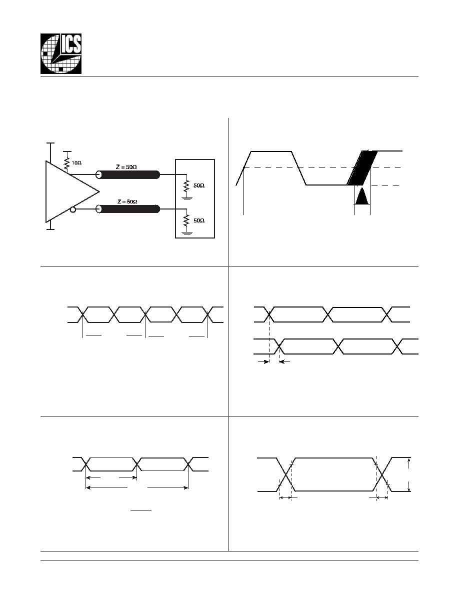
The clock layout topology shown below is a typical termina-
tion for LVPECL outputs. The two different layouts mentioned
are recommended only as guidelines.
FOUT and nFOUT are low impedance follower outputs that
generate ECL/LVPECL compatible outputs. Therefore, ter-
minating resistors (DC current path to ground) or current
sources must be used for functionality. These outputs are
F
IGURE
8B. LVPECL O
UTPUT
T
ERMINATION
F
IGURE
8A. LVPECL O
UTPUT
T
ERMINATION
designed to drive 50
transmission lines. Matched imped-
ance techniques should be used to maximize operating
frequency and minimize signal distortion.
Figures 8A and
8B
show two different layouts which are recommended only
as guidelines. Other suitable clock layouts may exist and it
would be recommended that the board designers simulate
to guarantee compatibility across all printed circuit and clock
component process variations.
T
ERMINATION
FOR
LVPECL O
UTPUTS

84330AY-03
www.icst.com/products/hiperclocks.html
REV. A FEBRUARY 2, 2006
16
Integrated
Circuit
Systems, Inc.
ICS84330-03
700MH
Z
, L
OW
J
ITTER
, C
RYSTAL
-
TO
-3.3V
D
IFFERENTIAL
LVPECL F
REQUENCY
S
YNTHESIZER
JA
by Velocity (Linear Feet per Minute)
0
200
500
Single-Layer PCB, JEDEC Standard Test Boards
67.8�C/W
55.9�C/W
50.1�C/W
Multi-Layer PCB, JEDEC Standard Test Boards
47.9�C/W
42.1�C/W
39.4�C/W
NOTE: Most modern PCB designs use multi-layered boards. The data in the second row pertains to most designs.
T
ABLE
9. T
HERMAL
R
ESISTANCE
JA
FOR
32-
PIN
LQFP, F
ORCED
C
ONVECTION
P
OWER
C
ONSIDERATIONS
This section provides information on power dissipation and junction temperature for the ICS84330-03.
Equations and example calculations are also provided.
1. Power Dissipation.
The total power dissipation for the ICS84330-03 is the sum of the core power plus the power dissipated in the load(s).
The following is the power dissipation for V
CC
= 3.3V + 5% = 3.465V, which gives worst case results.
NOTE: Please refer to Section 3 for details on calculating power dissipated in the load.
�
Power (core)
MAX
= V
CC_MAX
* I
EE_MAX
= 3.465V * 180mA = 623.7mW
�
Power (outputs)
MAX
= 30.2mW/Loaded Output pair
If all outputs are loaded, the total power is 2 * 30mW = 60mW
Total Power
_MAX
(3.465V, with all outputs switching) = 623.7 + 60mW = 683.7mW
2. Junction Temperature.
Junction temperature, Tj, is the temperature at the junction of the bond wire and bond pad and directly affects the reliability of the
device. The maximum recommended junction temperature for HiPerClockS
TM
devices is 125�C.
The equation for Tj is as follows: Tj =
JA
* Pd_total + T
A
Tj = Junction Temperature
JA
= Junction-to-Ambient Thermal Resistance
Pd_total = Total Device Power Dissipation (example calculation is in section 1 above)
T
A
= Ambient Temperature
In order to calculate junction temperature, the appropriate junction-to-ambient thermal resistance
JA
must be used. Assuming a
moderate air flow of 200 linear feet per minute and a multi-layer board, the appropriate value is 42.1�C/W per Table 9 below.
Therefore, Tj for an ambient temperature of 70�C with all outputs switching is:
70�C + 0.684W * 42.1�C/W = 98.8�C. This is well below the limit of 125�C.
This calculation is only an example. Tj will obviously vary depending on the number of loaded outputs, supply voltage, air flow,
and the type of board (single layer or multi-layer).

84330AY-03
www.icst.com/products/hiperclocks.html
REV. A FEBRUARY 2, 2006
17
Integrated
Circuit
Systems, Inc.
ICS84330-03
700MH
Z
, L
OW
J
ITTER
, C
RYSTAL
-
TO
-3.3V
D
IFFERENTIAL
LVPECL F
REQUENCY
S
YNTHESIZER
3. Calculations and Equations.
The purpose of this section is to derive the power dissipated into the load.
LVPECL output driver circuit and termination are shown in the
Figure 9.
T
o calculate worst case power dissipation into the load, use the following equations which assume a 50
load, and a termination
voltage of V
CC
- 2V.
�
For logic high, V
OUT
= V
OH_MAX
= V
CC_MAX
� 0.9V
(V
CC_MAX
- V
OH_MAX
) = 0.9V
�
For logic low, V
OUT
= V
OL_MAX
= V
CC_MAX
� 1.7V
(V
CC_MAX
- V
OL_MAX
) = 1.7V
Pd_H is power dissipation when the output drives high.
Pd_L is the power dissipation when the output drives low.
Pd_H = [(V
OH_MAX
� (V
CC_MAX
- 2V))/R
L
] * (V
CC_MAX
- V
OH_MAX
) = [(2V - (V
CC_MAX
- V
OH_MAX
))/R
L
] * (V
CC_MAX
- V
OH_MAX
) =
[(2V - 0.9V)/50
] * 0.9V = 19.8mW
Pd_L = [(V
OL_MAX
� (V
CC_MAX
- 2V))/R
L
] * (V
CC_MAX
- V
OL_MAX
) = [(2V - (V
CC_MAX
- V
OL_MAX
))/R
L
] * (V
CC_MAX
- V
OL_MAX
) =
[(2V - 1.7V)/50
] * 1.7V = 10.2mW
Total Power Dissipation per output pair = Pd_H + Pd_L = 30mW
F
IGURE
9. LVPECL D
RIVER
C
IRCUIT
AND
T
ERMINATION
Q1
V
OUT
V
CC
RL
50
V
CC
- 2V

84330AY-03
www.icst.com/products/hiperclocks.html
REV. A FEBRUARY 2, 2006
18
Integrated
Circuit
Systems, Inc.
ICS84330-03
700MH
Z
, L
OW
J
ITTER
, C
RYSTAL
-
TO
-3.3V
D
IFFERENTIAL
LVPECL F
REQUENCY
S
YNTHESIZER
R
ELIABILITY
I
NFORMATION
T
RANSISTOR
C
OUNT
The transistor count for ICS84330-03 is: 9304
JA
by Velocity (Linear Feet per Minute)
0
200
500
Single-Layer PCB, JEDEC Standard Test Boards
67.8�C/W
55.9�C/W
50.1�C/W
Multi-Layer PCB, JEDEC Standard Test Boards
47.9�C/W
42.1�C/W
39.4�C/W
NOTE: Most modern PCB designs use multi-layered boards. The data in the second row pertains to most designs.
T
ABLE
10.
JA
VS
. A
IR
F
LOW
32 L
EAD
LQFP T
ABLE

84330AY-03
www.icst.com/products/hiperclocks.html
REV. A FEBRUARY 2, 2006
19
Integrated
Circuit
Systems, Inc.
ICS84330-03
700MH
Z
, L
OW
J
ITTER
, C
RYSTAL
-
TO
-3.3V
D
IFFERENTIAL
LVPECL F
REQUENCY
S
YNTHESIZER
T
ABLE
11. P
ACKAGE
D
IMENSIONS
Reference Document: JEDEC Publication 95, MS-026
N
O
I
T
A
I
R
A
V
C
E
D
E
J
S
R
E
T
E
M
I
L
L
I
M
N
I
S
N
O
I
S
N
E
M
I
D
L
L
A
L
O
B
M
Y
S
A
B
B
M
U
M
I
N
I
M
L
A
N
I
M
O
N
M
U
M
I
X
A
M
N
2
3
A
-
-
-
-
0
6
.
1
1
A
5
0
.
0
-
-
5
1
.
0
2
A
5
3
.
1
0
4
.
1
5
4
.
1
b
0
3
.
0
7
3
.
0
5
4
.
0
c
9
0
.
0
-
-
0
2
.
0
D
C
I
S
A
B
0
0
.
9
1
D
C
I
S
A
B
0
0
.
7
2
D
.
f
e
R
0
6
.
5
E
C
I
S
A
B
0
0
.
9
1
E
C
I
S
A
B
0
0
.
7
2
E
.
f
e
R
0
6
.
5
e
C
I
S
A
B
0
8
.
0
L
5
4
.
0
0
6
.
0
5
7
.
0
0
�
-
-
7
�
c
c
c
-
-
-
-
0
1
.
0
P
ACKAGE
O
UTLINE
- Y S
UFFIX
FOR
32 L
EAD
LQFP

84330AY-03
www.icst.com/products/hiperclocks.html
REV. A FEBRUARY 2, 2006
20
Integrated
Circuit
Systems, Inc.
ICS84330-03
700MH
Z
, L
OW
J
ITTER
, C
RYSTAL
-
TO
-3.3V
D
IFFERENTIAL
LVPECL F
REQUENCY
S
YNTHESIZER
T
ABLE
12. O
RDERING
I
NFORMATION
While the information presented herein has been checked for both accuracy and reliability, Integrated Circuit Systems, Incorporated (ICS) assumes no responsibility for either its use
or for infringement of any patents or other rights of third parties, which would result from its use. No other circuits, patents, or licenses are implied. This product is intended for use
in normal commercial applications. Any other applications such as those requiring extended temperature range, high reliability, or other extraordinary environmental requirements are
not recommended without additional processing by ICS. ICS reserves the right to change any circuitry or specifications without notice. ICS does not authorize or warrant any ICS
product for use in life support devices or critical medical instruments.
The aforementioned trademark, HiPerClockS is a trademark of Integrated Circuit Systems, Inc. or its subsidiaries in the United States and/or other countries.
r
e
b
m
u
N
r
e
d
r
O
/
t
r
a
P
g
n
i
k
r
a
M
e
g
a
k
c
a
P
g
n
i
g
a
k
c
a
P
g
n
i
p
p
i
h
S
e
r
u
t
a
r
e
p
m
e
T
3
0
-
Y
A
0
3
3
4
8
S
C
I
3
0
Y
A
0
3
3
4
8
S
C
I
P
F
Q
L
d
a
e
L
2
3
y
a
r
T
C
�
0
7
o
t
C
�
0
T
3
0
-
Y
A
0
3
3
4
8
S
C
I
3
0
Y
A
0
3
3
4
8
S
C
I
P
F
Q
L
d
a
e
L
2
3
l
e
e
R
&
e
p
a
T
0
0
0
1
C
�
0
7
o
t
C
�
0
F
L
3
0
-
Y
A
0
3
3
4
8
S
C
I
L
3
0
A
0
3
3
4
8
S
C
I
P
F
Q
L
"
e
e
r
F
-
d
a
e
L
"
d
a
e
L
2
3
y
a
r
T
C
�
0
7
o
t
C
�
0
T
F
L
3
0
-
Y
A
0
3
3
4
8
S
C
I
L
3
0
A
0
3
3
4
8
S
C
I
P
F
Q
L
"
e
e
r
F
-
d
a
e
L
"
d
a
e
L
2
3
l
e
e
R
&
e
p
a
T
0
0
0
1
C
�
0
7
o
t
C
�
0
.
t
n
a
il
p
m
o
c
S
H
o
R
e
r
a
d
n
a
n
o
i
t
a
r
u
g
i
f
n
o
c
e
e
r
F
-
b
P
e
h
t
e
r
a
r
e
b
m
u
n
t
r
a
p
e
h
t
o
t
x
i
f
f
u
s
"
F
L
"
n
a
h
t
i
w
d
e
r
e
d
r
o
e
r
a
t
a
h
t
s
t
r
a
P
:
E
T
O
N