ChipFind - документация

Электронный компонент: ICS843404AG

Скачать:  PDF   ZIP
www.docs.chipfind.ru
background image
843404AG
www.icst.com/products/hiperclocks.html
REV. A OCTOBER 17, 2005
1
Integrated
Circuit
Systems, Inc.
ICS843404
LVCMOS/C
RYSTAL
-
TO
-3.3V LVPECL
AND
LVDS C
LOCK
G
ENERATOR
G
ENERAL
D
ESCRIPTION
The ICS843404 is a low phase noise Fibre
Channel Clock Generator and is a member of
the HiPerClockS
TM
family of high performance
clock solutions from ICS. The device provides
two banks of one LVPECL output per bank and
one bank of two LVDS outputs. Each bank can be
independently set by using their respective frequency select
pins for the following output frequencies: 318.75MHz,
212.5MHz, 159.375MHz or 106.25MHz, using a 25.5MHz
18pF parallel resonant crystal. The ICS843404 can also be
driven from a 25.5MHz single-ended reference clock. For
system debug or test purposes, the PLL can be bypassed
using the VCO_SEL pin.
F
EATURES
Three banks of outputs: one bank of two LVDS outputs
and two banks of one LVPECL output
Selectable crystal oscillator interface or
LVCMOS/LVTTL single-ended reference clock input
Four independently selectable output frequency on each
bank: 318.75MHz, 212.5MHz, 159.375MHz and 106.25MHz
Maximum output frequency: 318.75MHz
Crystal input frequency: 25.5MHz
V
DDO
_LVPECL can be set for 3.3V or 2.5V, allowing the
device to generate 3.3V or 2.5V LVPECL levels
RMS phase jitter at 106.25MHz, using a 25.5MHz crystal
(637kHz to 10MHz intergration): 2.65ps (typical)
Offset
Noise Power
100Hz ................. -89.1 dBc/Hz
1kHz ................. -112.7 dBc/Hz
10kHz ................. -128.0 dBc/Hz
100kHz ................. -130.2 dBc/Hz
Supply voltage modes:
V
DD
= V
DDA
= 3.3V
V
DDO_
LVPECL = 3.3V or 2.5V
V
DDO_
LVDS = 3.3V
0C to 70C ambient operating temperature
Available in both standard and lead-free RoHS-compliant
packages
Industrial termperature information available upon request
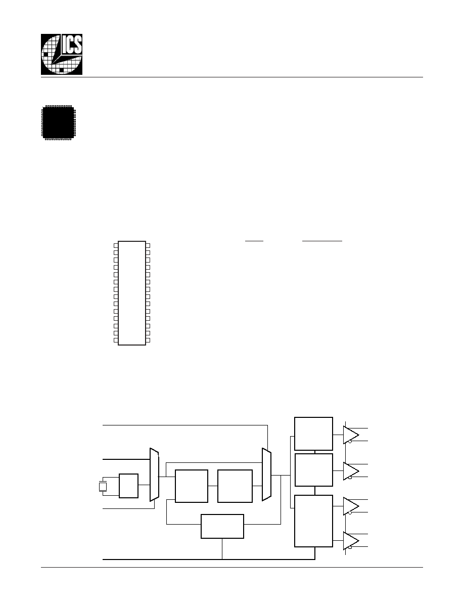
HiPerClockSTM
ICS
P
IN
A
SSIGNMENT
0
1
0
1
Phase
Detector
VCO
637.5MHz
(Fixed)
M = 25 (fixed)
LVDS_FSEL1:0
0 0 2
0 1 3
1 0 4
1 1 6
LVPECL_FSELA1:0
0 0 2
0 1 3
1 0 4
1 1 6
LVPECL_FSELB1:0
0 0 2
0 1 3
1 0 4
1 1 6
25.5MHz
V
DDO
_LVPECL
V
DDO
_LVDS
OSC
B
LOCK
D
IAGRAM
VCO_SEL
TEST_CLK
XTAL_IN
XTAL_OUT
XTAL_SEL
MR
LVPECLA0
nLVPECLA0
LVPECLB0
nLVPECLB0
LVDS0
nLVDS0
LVDS1
nLVDS1
Pullup
Pulldown
Pullup
Pulldown
ICS843404
28-Lead TSSOP, 173-MIL
4.4mm x 9.7mm x 0.92mm
body package
G Package
Top View
MR
VCO_SEL
V
DD
o_LVDS
LVDS0
nLVDS0
LVDS1
nLVDS1
nc
LVPECL_FSELB0
LVPECL_FSELB1
nc
V
DDA
LVPECL_FSELA0
V
DD
LVDS_FSEL0
LVDS_FSEL1
V
DDO
_LVPECL
LVPECLA0
nLVPECLA0
LVPECLB0
nLVPECLB0
XTAL_SEL
TEST_CLK
GND
GND
XTAL_IN
XTAL_OUT
LVPECL_FSELA1
1
2
3
4
5
6
7
8
9
10
11
12
13
14
28
27
26
25
24
23
22
21
20
19
18
17
16
15
background image
843404AG
www.icst.com/products/hiperclocks.html
REV. A OCTOBER 17, 2005
2
Integrated
Circuit
Systems, Inc.
ICS843404
LVCMOS/C
RYSTAL
-
TO
-3.3V LVPECL
AND
LVDS C
LOCK
G
ENERATOR
T
ABLE
1. P
IN
D
ESCRIPTIONS
T
ABLE
2. P
IN
C
HARACTERISTICS
r
e
b
m
u
N
e
m
a
N
e
p
y
T
n
o
i
t
p
i
r
c
s
e
D
1
R
M
t
u
p
n
I
n
w
o
d
ll
u
P
s
r
e
d
i
v
i
d
l
a
n
r
e
t
n
i
e
h
t
,
H
G
I
H
c
i
g
o
l
n
e
h
W
.
t
e
s
e
R
r
e
t
s
a
M
H
G
I
H
e
v
i
t
c
A
e
h
t
d
n
a
w
o
l
o
g
o
t
x
S
D
V
L
/
x
L
C
E
P
V
L
s
t
u
p
t
u
o
e
u
r
t
e
h
t
g
n
i
s
u
a
c
t
e
s
e
r
e
r
a
e
h
t
,
W
O
L
c
i
g
o
l
n
e
h
W
.
h
g
i
h
o
g
o
t
x
S
D
V
L
n
/
x
L
C
E
P
V
L
n
s
t
u
p
t
u
o
d
e
t
r
e
v
n
i
.
d
e
l
b
a
n
e
e
r
a
s
t
u
p
t
u
o
e
h
t
d
n
a
s
r
e
d
i
v
i
d
l
a
n
r
e
t
n
i
.
s
l
e
v
e
l
e
c
a
f
r
e
t
n
i
L
T
T
V
L
/
S
O
M
C
V
L
2
L
E
S
_
O
C
V
t
u
p
n
I
p
u
ll
u
P
n
i
s
i
L
L
P
,
W
O
L
n
e
h
W
.
d
e
l
b
a
n
e
s
i
L
L
P
,
H
G
I
H
n
e
h
W
.
n
i
p
t
c
e
l
e
s
O
C
V
.
s
l
e
v
e
l
e
c
a
f
r
e
t
n
i
L
T
T
V
L
/
S
O
M
C
V
L
.
e
d
o
m
s
s
a
p
y
B
3
V
O
D
D
S
D
V
L
_
r
e
w
o
P
.
s
t
u
p
t
u
o
S
D
V
L
r
o
f
n
i
p
y
l
p
p
u
s
t
u
p
t
u
O
5
,
4
0
S
D
V
L
n
,
0
S
D
V
L
t
u
p
t
u
O
.
s
l
e
v
e
l
e
c
a
f
r
e
t
n
i
S
D
V
L
.
r
i
a
p
t
u
p
t
u
o
l
a
i
t
n
e
r
e
f
f
i
D
7
,
6
1
S
D
V
L
n
,
1
S
D
V
L
t
u
p
t
u
O
.
s
l
e
v
e
l
e
c
a
f
r
e
t
n
i
S
D
V
L
.
r
i
a
p
t
u
p
t
u
o
l
a
i
t
n
e
r
e
f
f
i
D
1
1
,
8
c
n
d
e
s
u
n
U
.
t
c
e
n
n
o
c
o
N
9
0
B
L
E
S
F
_
L
C
E
P
V
L
t
u
p
n
I
n
w
o
d
ll
u
P
.
B
3
e
l
b
a
T
e
e
S
.
s
t
u
p
t
u
o
B
L
C
E
P
V
L
r
o
f
n
i
p
t
c
e
l
e
s
y
c
n
e
u
q
e
r
F
.
s
l
e
v
e
l
e
c
a
f
r
e
t
n
i
L
T
T
V
L
/
S
O
M
C
V
L
0
1
1
B
L
E
S
F
_
L
C
E
P
V
L
t
u
p
n
I
p
u
ll
u
P
.
B
3
e
l
b
a
T
e
e
S
.
s
t
u
p
t
u
o
B
L
C
E
P
V
L
r
o
f
n
i
p
t
c
e
l
e
s
y
c
n
e
u
q
e
r
F
.
s
l
e
v
e
l
e
c
a
f
r
e
t
n
i
L
T
T
V
L
/
S
O
M
C
V
L
2
1
V
A
D
D
r
e
w
o
P
.
n
i
p
y
l
p
p
u
s
g
o
l
a
n
A
3
1
0
A
L
E
S
F
_
L
C
E
P
V
L
t
u
p
n
I
n
w
o
d
ll
u
P
.
B
3
e
l
b
a
T
e
e
S
.
s
t
u
p
t
u
o
A
L
C
E
P
V
L
r
o
f
n
i
p
t
c
e
l
e
s
y
c
n
e
u
q
e
r
F
.
s
l
e
v
e
l
e
c
a
f
r
e
t
n
i
L
T
T
V
L
/
S
O
M
C
V
L
4
1
V
D
D
r
e
w
o
P
.
n
i
p
y
l
p
p
u
s
e
r
o
C
5
1
1
A
L
E
S
F
_
L
C
E
P
V
L
t
u
p
n
I
p
u
ll
u
P
.
B
3
e
l
b
a
T
e
e
S
.
s
t
u
p
t
u
o
A
L
C
E
P
V
L
r
o
f
n
i
p
t
c
e
l
e
s
y
c
n
e
u
q
e
r
F
.
s
l
e
v
e
l
e
c
a
f
r
e
t
n
i
L
T
T
V
L
/
S
O
M
C
V
L
7
1
,
6
1
,
T
U
O
_
L
A
T
X
N
I
_
L
A
T
X
t
u
p
n
I
,
t
u
p
n
i
e
h
t
s
i
N
I
_
L
A
T
X
.
e
c
a
f
r
e
t
n
i
l
a
t
s
y
r
c
t
n
a
n
o
s
e
r
l
e
ll
a
r
a
P
.
t
u
p
t
u
o
e
h
t
s
i
T
U
O
_
L
A
T
X
9
1
,
8
1
D
N
G
r
e
w
o
P
.
n
i
p
y
l
p
p
u
s
e
v
i
t
a
g
e
N
0
2
K
L
C
_
T
S
E
T
t
u
p
n
I
n
w
o
d
ll
u
P
.
t
u
p
n
i
k
c
o
l
c
L
T
T
V
L
/
S
O
M
C
V
L
1
2
L
E
S
_
L
A
T
X
t
u
p
n
I
p
u
ll
u
P
L
L
P
e
h
t
e
h
t
s
a
s
t
u
p
n
i
K
L
C
_
T
S
E
T
r
o
l
a
t
s
y
r
c
n
e
e
w
t
e
b
s
t
c
e
l
e
S
s
t
c
e
l
e
S
.
H
G
I
H
n
e
h
w
s
t
u
p
n
i
L
A
T
X
s
t
c
e
l
e
S
.
e
c
r
u
o
s
e
c
n
e
r
e
f
e
R
.
s
l
e
v
e
l
e
c
a
f
r
e
t
n
i
L
T
T
V
L
/
S
O
M
C
V
L
.
W
O
L
n
e
h
w
K
L
C
_
T
S
E
T
3
2
,
2
2
,
0
B
L
C
E
P
V
L
n
0
B
L
C
E
P
V
L
t
u
p
t
u
O
.
s
l
e
v
e
l
e
c
a
f
r
e
t
n
i
L
C
E
P
V
L
.
r
i
a
p
t
u
p
t
u
o
l
a
i
t
n
e
r
e
f
f
i
D
5
2
,
4
2
,
0
A
L
C
E
P
V
L
n
0
A
L
C
E
P
V
L
t
u
p
u
O
.
s
l
e
v
e
l
e
c
a
f
r
e
t
n
i
L
C
E
P
V
L
.
r
i
a
p
t
u
p
t
u
o
l
a
i
t
n
e
r
e
f
f
i
D
6
2
V
O
D
D
L
C
E
P
V
L
_
r
e
w
o
P
.
s
t
u
p
t
u
o
L
C
E
P
V
L
r
o
f
n
i
p
y
l
p
p
u
s
t
u
p
t
u
O
8
2
,
7
2
,
1
L
E
S
F
_
S
D
V
L
0
L
E
S
F
_
S
D
V
L
t
u
p
n
I
n
w
o
d
ll
u
P
.
A
3
e
l
b
a
T
e
e
S
.
s
t
u
p
t
u
o
S
D
V
L
r
o
f
s
n
i
p
t
c
e
l
e
s
y
c
n
e
u
q
e
r
F
.
s
l
e
v
e
l
e
c
a
f
r
e
t
n
i
L
T
T
V
L
/
S
O
M
C
V
L
:
E
T
O
N
n
w
o
d
ll
u
P
d
n
a
p
u
ll
u
P
.
s
e
u
l
a
v
l
a
c
i
p
y
t
r
o
f
,
s
c
i
t
s
i
r
e
t
c
a
r
a
h
C
n
i
P
,
2
e
l
b
a
T
e
e
S
.
s
r
o
t
s
i
s
e
r
t
u
p
n
i
l
a
n
r
e
t
n
i
o
t
r
e
f
e
r
l
o
b
m
y
S
r
e
t
e
m
a
r
a
P
s
n
o
i
t
i
d
n
o
C
t
s
e
T
m
u
m
i
n
i
M
l
a
c
i
p
y
T
m
u
m
i
x
a
M
s
t
i
n
U
C
N
I
e
c
n
a
t
i
c
a
p
a
C
t
u
p
n
I
4
F
p
R
P
U
L
L
U
P
r
o
t
s
i
s
e
R
p
u
ll
u
P
t
u
p
n
I
1
5
k
R
N
W
O
D
L
L
U
P
r
o
t
s
i
s
e
R
n
w
o
d
ll
u
P
t
u
p
n
I
1
5
k
background image
843404AG
www.icst.com/products/hiperclocks.html
REV. A OCTOBER 17, 2005
3
Integrated
Circuit
Systems, Inc.
ICS843404
LVCMOS/C
RYSTAL
-
TO
-3.3V LVPECL
AND
LVDS C
LOCK
G
ENERATOR
s
t
u
p
n
I
)
z
H
M
(
y
c
n
e
u
q
e
r
F
t
u
p
t
u
O
S
D
V
L
)
l
a
t
s
y
r
C
z
H
M
5
.
5
2
(
1
L
E
S
F
_
S
D
V
L
0
L
E
S
F
_
S
D
V
L
r
e
d
i
v
i
D
t
u
p
t
u
O
S
D
V
L
0
0
2
)
t
l
u
a
f
e
d
(
5
7
.
8
1
3
0
1
3
5
.
2
1
2
1
0
4
5
7
3
.
9
5
1
1
1
6
5
2
.
6
0
1
T
ABLE
3A. LVDS F
REQUENCY
S
ELECT
F
UNCTION
T
ABLE
s
t
u
p
n
I
0
A
L
C
E
P
V
L
)
z
H
M
(
y
c
n
e
u
q
e
r
F
t
u
p
t
u
O
)
l
a
t
s
y
r
C
z
H
M
5
.
5
2
(
1
A
L
E
S
F
_
L
C
E
P
V
L
0
A
L
E
S
F
_
L
C
E
P
V
L
0
A
L
C
E
P
V
L
r
e
d
i
v
i
D
t
u
p
t
u
O
0
0
2
5
7
.
8
1
3
0
1
3
5
.
2
1
2
1
0
4
)
t
l
u
a
f
e
d
(
5
7
3
.
9
5
1
1
1
6
5
2
.
6
0
1
T
ABLE
3B. LVPECLA0 F
REQUENCY
S
ELECT
F
UNCTION
T
ABLE
s
t
u
p
n
I
0
B
L
C
E
P
V
L
)
z
H
M
(
y
c
n
e
u
q
e
r
F
t
u
p
t
u
O
)
l
a
t
s
y
r
C
z
H
M
5
.
5
2
(
1
B
L
E
S
F
_
L
C
E
P
V
L
0
B
L
E
S
F
_
L
C
E
P
V
L
0
B
L
C
E
P
V
L
r
e
d
i
v
i
D
t
u
p
t
u
O
0
0
2
5
7
.
8
1
3
0
1
3
5
.
2
1
2
1
0
4
)
t
l
u
a
f
e
d
(
5
7
3
.
9
5
1
1
1
6
5
2
.
6
0
1
T
ABLE
3C. LVPECLB0 F
REQUENCY
S
ELECT
F
UNCTION
T
ABLE
background image
843404AG
www.icst.com/products/hiperclocks.html
REV. A OCTOBER 17, 2005
4
Integrated
Circuit
Systems, Inc.
ICS843404
LVCMOS/C
RYSTAL
-
TO
-3.3V LVPECL
AND
LVDS C
LOCK
G
ENERATOR
T
ABLE
4A. P
OWER
S
UPPLY
DC C
HARACTERISTICS
,
V
DD
= V
DDA
= V
DDO_LVPECL
= V
DDO_LVDS
= 3.3V5%, TA = 0C
TO
70C
A
BSOLUTE
M
AXIMUM
R
ATINGS
Supply Voltage, V
DD
4.6V
Inputs, V
I
-0.5V to V
DD
+ 0.5V
Outputs, I
O
(LVPECL Outputs)
Continuous Current
50mA
Surge Current
100mA
Outputs, I
O
(LVDS Outputs)
Continuous Current
10mA
Surge Current
15mA
Package Thermal Impedance,
JA
49.8C/W (0 lfpm)
Storage Temperature, T
STG
-65C to 150C
NOTE: Stresses beyond those listed under Absolute
Maximum Ratings may cause permanent damage to the
device. These ratings are stress specifications only. Functional
operation of product at these conditions or any conditions be-
yond those listed in the
DC Characteristics
or
AC Character-
istics
is not implied. Exposure to absolute maximum rating
conditions for extended periods may affect product reliability.
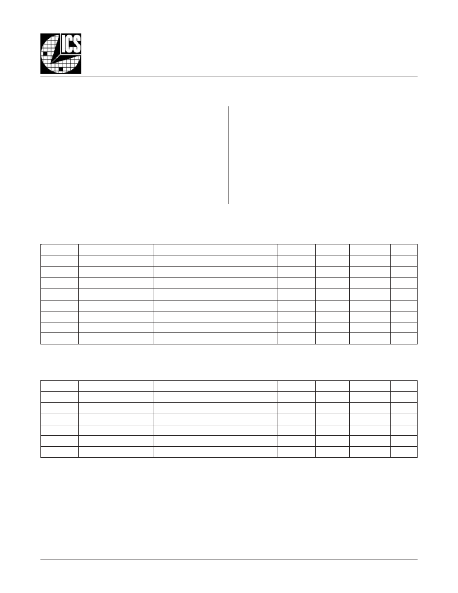
T
ABLE
4B. P
OWER
S
UPPLY
DC C
HARACTERISTICS
,
V
DD
= V
DDA
= 3.3V5%, V
DDO_LVPECL
= 2.5V5%, TA = 0C
TO
70C
l
o
b
m
y
S
r
e
t
e
m
a
r
a
P
s
n
o
i
t
i
d
n
o
C
t
s
e
T
m
u
m
i
n
i
M
l
a
c
i
p
y
T
m
u
m
i
x
a
M
s
t
i
n
U
V
D
D
e
g
a
t
l
o
V
y
l
p
p
u
S
e
r
o
C
5
3
1
.
3
3
.
3
5
6
4
.
3
V
V
A
D
D
e
g
a
t
l
o
V
y
l
p
p
u
S
g
o
l
a
n
A
5
3
1
.
3
3
.
3
5
6
4
.
3
V
V
L
C
E
P
V
L
_
O
D
D
e
g
a
t
l
o
V
y
l
p
p
u
S
t
u
p
t
u
O
5
3
1
.
3
3
.
3
5
6
4
.
3
V
V
S
D
V
L
_
O
D
D
e
g
a
t
l
o
V
y
l
p
p
u
S
t
u
p
t
u
O
5
3
1
.
3
3
.
3
5
6
4
.
3
V
I
D
D
t
n
e
r
r
u
C
y
l
p
p
u
S
r
e
w
o
P
0
0
1
A
m
I
A
D
D
t
n
e
r
r
u
C
y
l
p
p
u
S
g
o
l
a
n
A
5
2
A
m
I
L
C
E
P
V
L
_
O
D
D
t
n
e
r
r
u
C
y
l
p
p
u
S
t
u
p
t
u
O
0
2
A
m
I
S
D
V
L
_
O
D
D
t
n
e
r
r
u
C
y
l
p
p
u
S
t
u
p
t
u
O
5
5
A
m
l
o
b
m
y
S
r
e
t
e
m
a
r
a
P
s
n
o
i
t
i
d
n
o
C
t
s
e
T
m
u
m
i
n
i
M
l
a
c
i
p
y
T
m
u
m
i
x
a
M
s
t
i
n
U
V
D
D
e
g
a
t
l
o
V
y
l
p
p
u
S
e
r
o
C
5
3
1
.
3
3
.
3
5
6
4
.
3
V
V
A
D
D
e
g
a
t
l
o
V
y
l
p
p
u
S
g
o
l
a
n
A
5
3
1
.
3
3
.
3
5
6
4
.
3
V
V
L
C
E
P
V
L
_
O
D
D
e
g
a
t
l
o
V
y
l
p
p
u
S
t
u
p
t
u
O
5
7
3
.
2
5
.
2
5
2
6
.
2
V
I
D
D
t
n
e
r
r
u
C
y
l
p
p
u
S
r
e
w
o
P
0
7
A
m
I
A
D
D
t
n
e
r
r
u
C
y
l
p
p
u
S
g
o
l
a
n
A
0
2
A
m
I
L
C
E
P
V
L
_
O
D
D
t
n
e
r
r
u
C
y
l
p
p
u
S
t
u
p
t
u
O
0
2
A
m
background image
843404AG
www.icst.com/products/hiperclocks.html
REV. A OCTOBER 17, 2005
5
Integrated
Circuit
Systems, Inc.
ICS843404
LVCMOS/C
RYSTAL
-
TO
-3.3V LVPECL
AND
LVDS C
LOCK
G
ENERATOR
T
ABLE
4C. LVCMOS / LVTTL DC C
HARACTERISTICS
,
V
DD
= V
DD
A
= V
DDO_LVPECL
= V
DDO_LVDS
= 3.3V5%,
V
DD
= V
DD
A
= 3.3V5%, V
DDO_LVPECL
= 2.5V5%, TA = 0C
TO
70C
T
ABLE
4D. LVPECL DC C
HARACTERISTICS
,
V
DD
= V
DDA
= 3.3V5%, V
DDO_LVPECL
= 3.3V5%
OR
2.5V5%, TA = 0C
TO
70C
T
ABLE
4E. LVDS DC C
HARACTERISTICS
,
V
DD
= V
DDA
= V
DDO_LVDS
= 3.3V5%, TA = 0C
TO
70C
l
o
b
m
y
S
r
e
t
e
m
a
r
a
P
s
n
o
i
t
i
d
n
o
C
t
s
e
T
m
u
m
i
n
i
M
l
a
c
i
p
y
T
m
u
m
i
x
a
M
s
t
i
n
U
V
D
O
e
g
a
t
l
o
V
t
u
p
t
u
O
l
a
i
t
n
e
r
e
f
f
i
D
0
5
3
V
m
V
D
O
V
D
O
e
g
n
a
h
C
e
d
u
t
i
n
g
a
M
4
V
m
V
S
O
e
g
a
t
l
o
V
t
e
s
f
f
O
5
3
.
1
V
V
S
O
V
S
O
e
g
n
a
h
C
e
d
u
t
i
n
g
a
M
5
V
m
T
ABLE
5. C
RYSTAL
C
HARACTERISTICS
l
o
b
m
y
S
r
e
t
e
m
a
r
a
P
s
n
o
i
t
i
d
n
o
C
t
s
e
T
m
u
m
i
n
i
M
l
a
c
i
p
y
T
m
u
m
i
x
a
M
s
t
i
n
U
V
H
I
e
g
a
t
l
o
V
h
g
i
H
t
u
p
n
I
2
V
D
D
3
.
0
+
V
V
L
I
e
g
a
t
l
o
V
w
o
L
t
u
p
n
I
3
.
0
-
8
.
0
V
I
H
I
t
u
p
n
I
t
n
e
r
r
u
C
h
g
i
H
,
R
M
,
K
L
C
_
T
S
E
T
,
0
A
L
E
S
F
_
L
C
E
P
V
L
,
0
B
L
E
S
F
_
L
C
E
P
V
L
1
L
E
S
F
_
S
D
V
L
,
0
L
E
S
F
_
S
D
V
L
V
D
D
V
=
N
I
V
5
6
4
.
3
=
0
5
1
A
,
1
A
L
E
S
F
_
L
C
E
P
V
L
,
1
B
L
E
S
F
_
L
C
E
P
V
L
L
E
S
_
L
A
T
X
,
L
E
S
_
O
C
V
V
D
D
V
=
N
I
V
5
6
4
.
3
=
5
A
I
L
I
t
u
p
n
I
t
n
e
r
r
u
C
w
o
L
,
R
M
,
K
L
C
_
T
S
E
T
,
0
A
L
E
S
F
_
L
C
E
P
V
L
,
0
B
L
E
S
F
_
L
C
E
P
V
L
1
L
E
S
F
_
S
D
V
L
,
0
L
E
S
F
_
S
D
V
L
V
D
D
V
,
V
5
6
4
.
3
=
N
I
V
0
=
5
-
A
,
1
A
L
E
S
F
_
L
C
E
P
V
L
,
1
B
L
E
S
F
_
L
C
E
P
V
L
L
E
S
_
L
A
T
X
,
L
E
S
_
O
C
V
V
D
D
V
,
V
5
6
4
.
3
=
N
I
V
0
=
0
5
1
-
A
l
o
b
m
y
S
r
e
t
e
m
a
r
a
P
s
n
o
i
t
i
d
n
o
C
t
s
e
T
m
u
m
i
n
i
M
l
a
c
i
p
y
T
m
u
m
i
x
a
M
s
t
i
n
U
V
H
O
1
E
T
O
N
;
e
g
a
t
l
o
V
h
g
i
H
t
u
p
t
u
O
V
L
C
E
P
V
L
_
O
D
D
4
.
1
-
V
L
C
E
P
V
L
_
O
D
D
9
.
0
-
V
V
L
O
1
E
T
O
N
;
e
g
a
t
l
o
V
w
o
L
t
u
p
t
u
O
V
L
C
E
P
V
L
_
O
D
D
0
.
2
-
V
L
C
E
P
V
L
_
O
D
D
7
.
1
-
V
V
G
N
I
W
S
g
n
i
w
S
e
g
a
t
l
o
V
t
u
p
t
u
O
k
a
e
P
-
o
t
-
k
a
e
P
6
.
0
0
.
1
V
0
5
h
t
i
w
d
e
t
a
n
i
m
r
e
t
s
t
u
p
t
u
O
:
1
E
T
O
N
V
o
t
L
C
E
P
V
L
_
O
D
D
.
V
2
-
r
e
t
e
m
a
r
a
P
s
n
o
i
t
i
d
n
o
C
t
s
e
T
m
u
m
i
n
i
M
l
a
c
i
p
y
T
m
u
m
i
x
a
M
s
t
i
n
U
n
o
i
t
a
ll
i
c
s
O
f
o
e
d
o
M
l
a
t
n
e
m
a
d
n
u
F
y
c
n
e
u
q
e
r
F
5
.
5
2
z
H
M
)
R
S
E
(
e
c
n
a
t
s
i
s
e
R
s
e
i
r
e
S
t
n
e
l
a
v
i
u
q
E
0
5
e
c
n
a
t
i
c
a
p
a
C
t
n
u
h
S
7
F
p
l
e
v
e
L
e
v
i
r
D
1
W
m
.
l
a
t
s
y
r
c
t
n
a
n
o
s
e
r
l
e
ll
a
r
a
p
F
p
8
1
n
a
g
n
i
s
u
d
e
z
i
r
e
t
c
a
r
a
h
C
:
E
T
O
N

Document Outline