Document Outline
- General Description
- Features
- Block Diagram
- Pin Assignment
- Pin Descriptions
- Pin Characteristics
- Output Configuration and Frequency Range Function Table
- Absolute Maximum Ratings
- Power Supply DC Characteristics
- LVCMOS DC Characteristics
- LVDS DC Characteristics
- Crystal Characteristics
- AC Characteristics
- Typical Phase Noise Plot @ 155.52MHz
- Typical Phase Noise Plot @ 622.08MHz
- Parameter Measurement Information
- Application Information
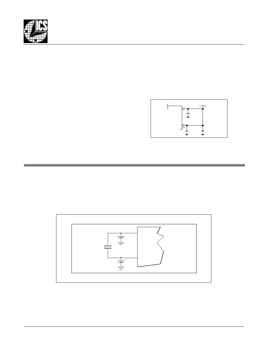
- Power Supply Filtering Techniques
- Crystal Input Interface
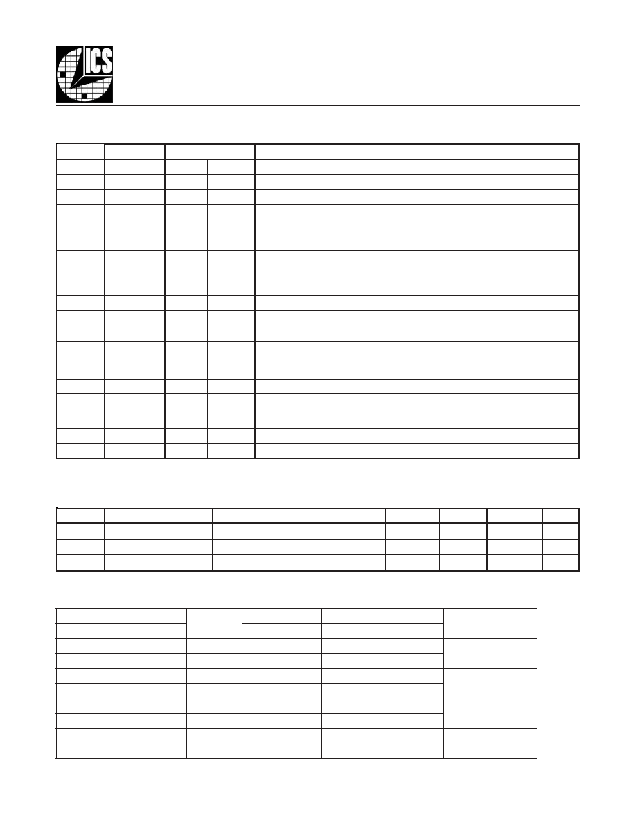
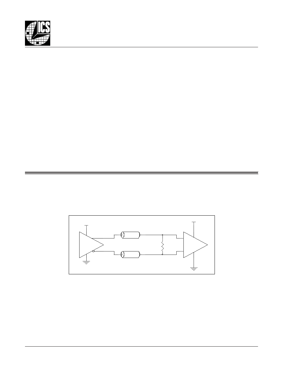
- 3.3V LVDS Driver Termination
- Recommendations for Unused Input and Output Pins
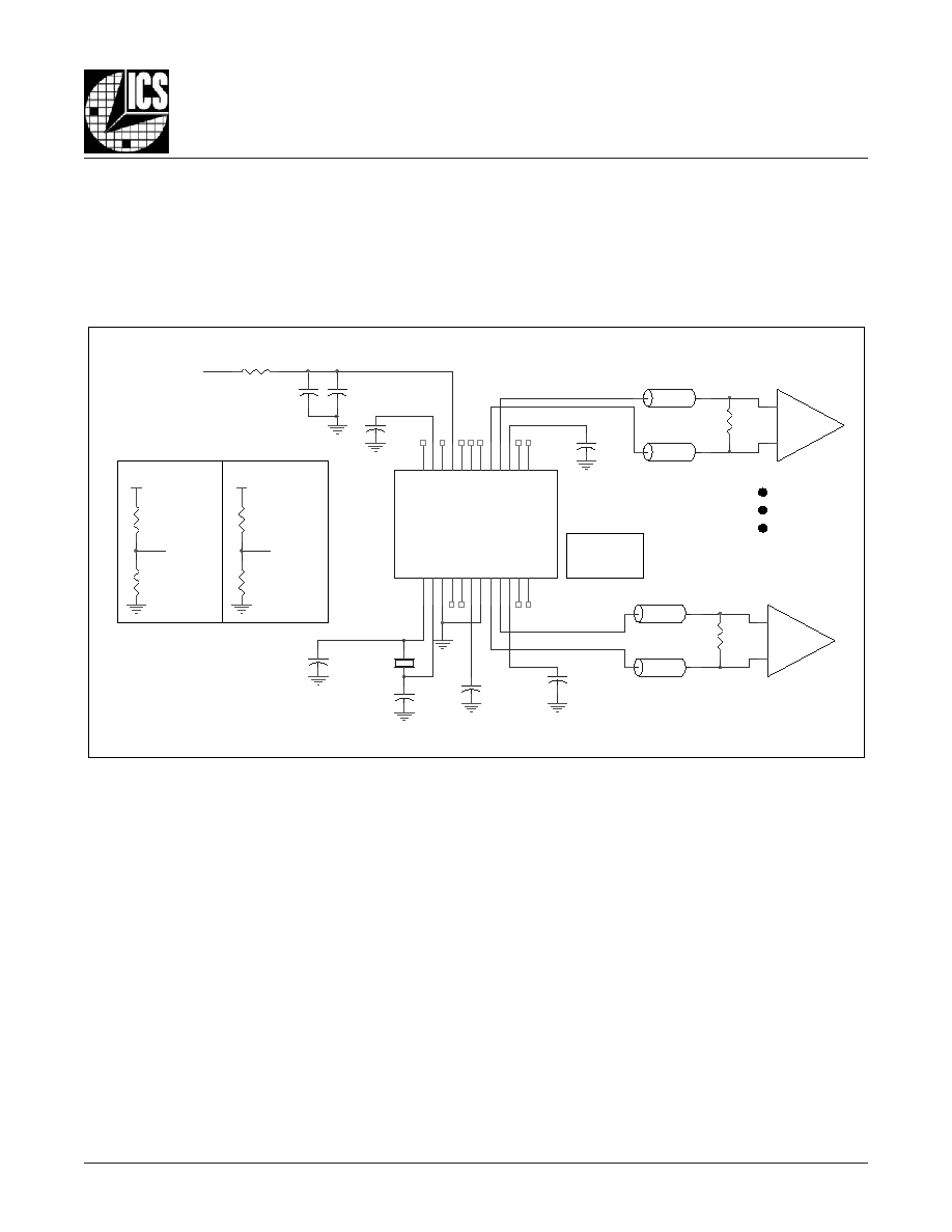
- Schematic Example
- Power Considerations
- Power Dissipation
- Junction Temperature
- Thermal Resistance
- Reliability Information
- Transistor Count
- Package Outline
- Package Dimensions
- Ordering Information

844004AGI-04
www.icst.com/products/hiperclocks.html
REV. A JANUARY 26, 2006
1
Integrated
Circuit
Systems, Inc.
ICS844004I-04
F
EMTO
C
LOCKS
TM C
RYSTAL
/LVCMOS-
TO
-
LVDS F
REQUENCY
S
YNTHESIZER
PRELIMINARY
0
1
Phase
Detector
VCO
M = �32
OSC
�4
�1
0
1
0
1
0
1
0
1
G
ENERAL
D
ESCRIPTION
T h e I C S 8 4 4 0 0 4 I - 0 4 i s a 4 o u t p u t LV D S
Synthesizer optimized to generate clock
frequencies for a variety of high performance
a p p l i c a t i o n s a n d i s a m e m b e r o f t h e
HiPerClocks
TM
family of high perfor mance
clock solutions from ICS. This device can select its input
reference clock from either a crystal input or a single-
ended clock signal. It can be configured to generate 4
outputs with individually selectable divide-by-one or
divide-by-four function via the 4 frequency select pins
(F_SEL[3:0]). The ICS844004I-04 uses ICS' 3
rd
generation
low phase noise VCO technology and can achieve 1ps
or lower typical r ms phase jitter. This ensures that it
will easily meet clocking requirements for SDH (STM-1/
STM-4/STM-16) and SONET (OC-3/OC12/OC-48). This
device is suitable for multi-rate and multiple por t line
card applications. The ICS844004I-04 is conveniently
packaged in a small 24-pin TSSOP package.
F
EATURES
� Four LVDS outputs
� Selectable crystal oscillator interface
or LVCMOS/LVTTL single-ended input
� Supports the following applications: SONET/SDH, SATA,
or 10Gb Ethernet
� Output frequency range: 140MHz - 170MHz,
560MHz - 680MHz
� VCO range: 560MHz - 680MHz
� Crystal oscillator and CLK range: 17.5MHz - 21.25MHz
� RMS phase jitter @ 622.08MHz output, using a 19.44MHz
crystal (12kHz - 20MHz): 0.71ps (typical)
� RMS phase jitter @ 156.25MHz output, using a 19.53125MHz
crystal (1.875MHz - 20MHz): 0.51ps (typical)
� RMS phase jitter @ 155.52MHz output, using a 19.44MHz
crystal (12kHz - 5MHz): 0.75ps (typical)
� Full 3.3V supply mode
� -40�C to 85�C ambient operating temperature
� Available in both standard and lead-free RoHS compliant
packages
HiPerClockSTM
ICS
P
IN
A
SSIGNMENT
ICS844004I-04
24-Lead TSSOP
4.40mm x 7.8mm x 0.92mm
package body
G Package
Top View
nQ1
Q1
V
DD
o
Q0
nQ0
MR
F_SEL3
nc
V
DDA
F_SEL0
V
DD
F_SEL1
1
2
3
4
5
6
7
8
9
10
11
12
nQ2
Q2
V
DDO
Q3
nQ3
GND
F_SEL2
INPUT_SEL
CLK
GND
XTAL_IN
XTAL_OUT
24
23
22
21
20
19
18
17
16
15
14
13
B
LOCK
D
IAGRAM
CLK
INPUT_SEL
MR
F_SEL0
F_SEL1
F_SEL2
F_SEL3
Q0
nQ0
Q1
nQ1
Q2
nQ2
Q3
nQ3
Pulldown
Pulldown
Pulldown
Pullup
Pullup
Pullup
Pullup
XTAL_IN
XTAL_OUT
The Preliminary Information presented herein represents a product in prototyping or pre-production. The noted characteristics are based on initial
product characterization. Integrated Circuit Systems, Incorporated (ICS) reserves the right to change any circuitry or specifications without notice.
844004AGI-04
www.icst.com/products/hiperclocks.html
REV. A JANUARY 26, 2006
2
Integrated
Circuit
Systems, Inc.
ICS844004I-04
F
EMTO
C
LOCKS
TM C
RYSTAL
/LVCMOS-
TO
-
LVDS F
REQUENCY
S
YNTHESIZER
PRELIMINARY
T
ABLE
1. P
IN
D
ESCRIPTIONS
T
ABLE
2. P
IN
C
HARACTERISTICS
r
e
b
m
u
N
e
m
a
N
e
p
y
T
n
o
i
t
p
i
r
c
s
e
D
2
,
1
1
Q
,
1
Q
n
t
u
p
t
u
O
.
s
l
e
v
e
l
e
c
a
f
r
e
t
n
i
S
D
V
L
.
r
i
a
p
t
u
p
t
u
o
l
a
i
t
n
e
r
e
f
f
i
D
2
2
,
3
V
O
D
D
r
e
w
o
P
.
s
n
i
p
y
l
p
p
u
s
t
u
p
t
u
O
5
,
4
0
Q
n
,
0
Q
t
u
p
u
O
.
s
l
e
v
e
l
e
c
a
f
r
e
t
n
i
S
D
V
L
.
r
i
a
p
t
u
p
t
u
o
l
a
i
t
n
e
r
e
f
f
i
D
6
R
M
t
u
p
n
I
n
w
o
d
ll
u
P
e
r
a
s
r
e
d
i
v
i
d
l
a
n
r
e
t
n
i
e
h
t
,
H
G
I
H
c
i
g
o
l
n
e
h
W
.
t
e
s
e
R
r
e
t
s
a
M
H
G
I
H
e
v
i
t
c
A
x
Q
n
s
t
u
p
t
u
o
d
e
t
r
e
v
n
i
e
h
t
d
n
a
w
o
l
o
g
o
t
x
Q
s
t
u
p
t
u
o
e
u
r
t
e
h
t
g
n
i
s
u
a
c
t
e
s
e
r
e
r
a
s
t
u
p
t
u
o
e
h
t
d
n
a
s
r
e
d
i
v
i
d
l
a
n
r
e
t
n
i
e
h
t
,
W
O
L
c
i
g
o
l
n
e
h
W
.
h
g
i
h
o
g
o
t
.
s
l
e
v
e
l
e
c
a
f
r
e
t
n
i
L
T
T
V
L
/
S
O
M
C
V
L
.
d
e
l
b
a
n
e
,
7
,
0
1
,
2
1
8
1
,
3
L
E
S
_
F
,
0
L
E
S
_
F
,
1
L
E
S
_
F
2
L
E
S
_
F
t
u
p
n
I
p
u
ll
u
P
.
3
e
l
b
a
T
e
e
S
.
s
l
e
v
e
l
e
c
a
f
r
e
t
n
i
L
T
T
V
L
/
S
O
M
C
V
L
.
s
n
i
p
t
c
e
l
e
s
y
c
n
e
u
q
e
r
F
8
c
n
d
e
s
u
n
U
.
t
c
e
n
n
o
c
o
N
9
V
A
D
D
r
e
w
o
P
.
n
i
p
y
l
p
p
u
s
g
o
l
a
n
A
1
1
V
D
D
r
e
w
o
P
.
n
i
p
y
l
p
p
u
s
e
r
o
C
4
1
,
3
1
,
T
U
O
_
L
A
T
X
N
I
_
L
A
T
X
t
u
p
n
I
,
t
u
p
t
u
o
e
h
t
s
i
T
U
O
_
L
A
T
X
.
e
c
a
f
r
e
t
n
i
l
a
t
s
y
r
c
t
n
a
n
o
s
e
r
l
e
ll
a
r
a
P
.
t
u
p
n
i
e
h
t
s
i
N
I
_
L
A
T
X
9
1
,
5
1
D
N
G
r
e
w
o
P
.
d
n
u
o
r
g
y
l
p
p
u
s
r
e
w
o
P
6
1
K
L
C
t
u
p
n
I
n
w
o
d
ll
u
P
.
t
u
p
n
i
k
c
o
l
c
L
T
T
V
L
/
S
O
M
C
V
L
7
1
L
E
S
_
T
U
P
N
I
t
u
p
n
I
n
w
o
d
ll
u
P
.
e
c
r
u
o
s
e
c
n
e
r
e
f
e
R
L
L
P
e
h
t
e
h
t
s
a
s
t
u
p
n
i
K
L
C
r
o
l
a
t
s
y
r
c
n
e
e
w
t
e
b
s
t
c
e
l
e
S
.
H
G
I
H
n
e
h
w
K
L
C
s
t
c
e
l
e
S
.
W
O
L
n
e
h
w
s
t
u
p
n
i
L
A
T
X
s
t
c
e
l
e
S
.
s
l
e
v
e
l
e
c
a
f
r
e
t
n
i
L
T
T
V
L
/
S
O
M
C
V
L
1
2
,
0
2
3
Q
,
3
Q
n
t
u
p
t
u
O
.
s
l
e
v
e
l
e
c
a
f
r
e
t
n
i
S
D
V
L
.
r
i
a
p
t
u
p
t
u
o
l
a
i
t
n
e
r
e
f
f
i
D
4
2
,
3
2
2
Q
n
,
2
Q
t
u
p
t
u
O
.
s
l
e
v
e
l
e
c
a
f
r
e
t
n
i
S
D
V
L
.
r
i
a
p
t
u
p
t
u
o
l
a
i
t
n
e
r
e
f
f
i
D
:
E
T
O
N
p
u
ll
u
P
d
n
a
n
w
o
d
ll
u
P
.
s
e
u
l
a
v
l
a
c
i
p
y
t
r
o
f
,
s
c
i
t
s
i
r
e
t
c
a
r
a
h
C
n
i
P
,
2
e
l
b
a
T
e
e
S
.
s
r
o
t
s
i
s
e
r
t
u
p
n
i
l
a
n
r
e
t
n
i
o
t
r
e
f
e
r
l
o
b
m
y
S
r
e
t
e
m
a
r
a
P
s
n
o
i
t
i
d
n
o
C
t
s
e
T
m
u
m
i
n
i
M
l
a
c
i
p
y
T
m
u
m
i
x
a
M
s
t
i
n
U
C
N
I
e
c
n
a
t
i
c
a
p
a
C
t
u
p
n
I
4
F
p
R
N
W
O
D
L
L
U
P
r
o
t
s
i
s
e
R
n
w
o
d
ll
u
P
t
u
p
n
I
1
5
k
R
P
U
L
L
U
P
r
o
t
s
i
s
e
R
p
u
ll
u
P
t
u
p
n
I
1
5
k
T
ABLE
3. O
UTPUT
C
ONFIGURATION
AND
F
REQUENCY
R
ANGE
F
UNCTION
T
ABLE
s
t
u
p
n
I
O
C
V
)
z
H
M
(
e
u
l
a
V
r
e
d
i
v
i
D
N
)
z
H
M
(
y
c
n
e
u
q
e
r
F
t
u
p
t
u
O
n
o
i
t
a
c
i
l
p
p
A
x
L
E
S
_
F
)
z
H
M
(
L
A
T
X
3
N
:
0
N
3
Q
n
/
3
Q
:
0
Q
n
/
0
Q
0
4
4
.
9
1
8
0
.
2
2
6
1
8
0
.
2
2
6
H
D
S
/
T
E
N
O
S
1
4
4
.
9
1
8
0
.
2
2
6
4
2
5
.
5
5
1
0
5
7
.
8
1
0
0
6
1
0
0
6
A
T
A
S
1
5
7
.
8
1
0
0
6
4
0
5
1
0
5
2
1
3
5
.
9
1
5
2
6
1
5
2
6
t
e
n
r
e
h
t
E
t
i
b
a
g
i
G
0
1
1
5
2
1
3
5
.
9
1
5
2
6
4
5
2
.
6
5
1
0
1
0
6
1
4
1
.
0
2
2
1
3
5
.
4
4
6
1
2
1
3
5
.
4
4
6
t
e
n
r
e
h
t
E
t
i
b
a
g
i
G
0
1
C
E
F
B
4
6
/
B
6
6
1
1
0
6
1
4
1
.
0
2
2
1
3
5
.
4
4
6
4
3
1
.
1
6
1
844004AGI-04
www.icst.com/products/hiperclocks.html
REV. A JANUARY 26, 2006
3
Integrated
Circuit
Systems, Inc.
ICS844004I-04
F
EMTO
C
LOCKS
TM C
RYSTAL
/LVCMOS-
TO
-
LVDS F
REQUENCY
S
YNTHESIZER
PRELIMINARY
A
BSOLUTE
M
AXIMUM
R
ATINGS
Supply Voltage, V
CC
4.6V
Inputs, V
I
-0.5V to V
CC
+ 0.5V
Outputs, I
O
Continuous Current
10mA
Surge Current
15mA
Package Thermal Impedance,
JA
70�C/W (0 mps)
Storage Temperature, T
STG
-65�C to 150�C
NOTE: Stresses beyond those listed under Absolute
Maximum Ratings may cause permanent damage to the
device. These ratings are stress specifications only. Functional
operation of product at these conditions or any conditions be-
yond those listed in the
DC Characteristics
or
AC Character-
istics
is not implied. Exposure to absolute maximum rating
conditions for extended periods may affect product reliability.
T
ABLE
4A. P
OWER
S
UPPLY
DC C
HARACTERISTICS
,
V
DD
= V
DDA
= V
DDO
= 3.3V�5%, TA = -40�C
TO
85�C
T
ABLE
4B. LVCMOS / LVTTL DC C
HARACTERISTICS
,
V
DD
= V
DDA
= V
DDO
= 3.3V�5%, TA = -40�C
TO
85�C
l
o
b
m
y
S
r
e
t
e
m
a
r
a
P
s
n
o
i
t
i
d
n
o
C
t
s
e
T
m
u
m
i
n
i
M
l
a
c
i
p
y
T
m
u
m
i
x
a
M
s
t
i
n
U
V
H
I
e
g
a
t
l
o
V
h
g
i
H
t
u
p
n
I
2
V
D
D
3
.
0
+
V
V
L
I
e
g
a
t
l
o
V
w
o
L
t
u
p
n
I
3
.
0
-
8
.
0
V
I
H
I
t
n
e
r
r
u
C
h
g
i
H
t
u
p
n
I
,
K
L
C
L
E
S
_
T
U
P
N
I
,
R
M
V
D
D
V
=
N
I
5
6
4
.
3
=
0
5
1
A
�
3
L
E
S
_
F
:
0
L
E
S
_
F
V
D
D
V
=
N
I
5
6
4
.
3
=
5
A
�
I
L
I
t
n
e
r
r
u
C
w
o
L
t
u
p
n
I
,
K
L
C
L
E
S
_
T
U
P
N
I
,
R
M
V
D
D
V
,
V
5
6
4
.
3
=
N
I
V
0
=
5
-
A
�
3
L
E
S
_
F
:
0
L
E
S
_
F
V
D
D
V
,
V
5
6
4
.
3
=
N
I
V
0
=
0
5
1
-
A
�
/
V
T
e
t
a
R
e
g
d
E
t
u
p
n
I
K
L
C
%
0
8
-
%
0
2
D
B
T
s
n
/
V
l
o
b
m
y
S
r
e
t
e
m
a
r
a
P
s
n
o
i
t
i
d
n
o
C
t
s
e
T
m
u
m
i
n
i
M
l
a
c
i
p
y
T
m
u
m
i
x
a
M
s
t
i
n
U
V
D
D
e
g
a
t
l
o
V
y
l
p
p
u
S
e
r
o
C
5
3
1
.
3
3
.
3
5
6
4
.
3
V
V
A
D
D
e
g
a
t
l
o
V
y
l
p
p
u
S
g
o
l
a
n
A
5
3
1
.
3
3
.
3
5
6
4
.
3
V
V
O
D
D
e
g
a
t
l
o
V
y
l
p
p
u
S
t
u
p
t
u
O
5
3
1
.
3
3
.
3
5
6
4
.
3
V
I
D
D
t
n
e
r
r
u
C
y
l
p
p
u
S
r
e
w
o
P
0
8
A
m
I
A
D
D
t
n
e
r
r
u
C
y
l
p
p
u
S
g
o
l
a
n
A
8
A
m
I
O
D
D
t
n
e
r
r
u
C
y
l
p
p
u
S
t
u
p
t
u
O
7
8
A
m
T
ABLE
4C. LVDS DC C
HARACTERISTICS
,
V
DD
= V
DDA
= V
DDO
= 3.3V�5%, TA = -40�C
TO
85�C
l
o
b
m
y
S
r
e
t
e
m
a
r
a
P
s
n
o
i
t
i
d
n
o
C
t
s
e
T
m
u
m
i
n
i
M
l
a
c
i
p
y
T
m
u
m
i
x
a
M
s
t
i
n
U
V
D
O
e
g
a
t
l
o
V
t
u
p
t
u
O
l
a
i
t
n
e
r
e
f
f
i
D
0
5
3
V
m
V
D
O
V
D
O
e
g
n
a
h
C
e
d
u
t
i
n
g
a
M
0
4
V
m
V
S
O
e
g
a
t
l
o
V
t
e
s
f
f
O
5
3
.
1
V
V
S
O
V
S
O
e
g
n
a
h
C
e
d
u
t
i
n
g
a
M
0
5
V
m
844004AGI-04
www.icst.com/products/hiperclocks.html
REV. A JANUARY 26, 2006
4
Integrated
Circuit
Systems, Inc.
ICS844004I-04
F
EMTO
C
LOCKS
TM C
RYSTAL
/LVCMOS-
TO
-
LVDS F
REQUENCY
S
YNTHESIZER
PRELIMINARY
T
ABLE
6. AC C
HARACTERISTICS
,
V
DD
= V
DDA
= V
DDO
= 3.3V�5%, TA = -40�C
TO
85�C
T
ABLE
5. C
RYSTAL
C
HARACTERISTICS
r
e
t
e
m
a
r
a
P
s
n
o
i
t
i
d
n
o
C
t
s
e
T
m
u
m
i
n
i
M
l
a
c
i
p
y
T
m
u
m
i
x
a
M
s
t
i
n
U
n
o
i
t
a
ll
i
c
s
O
f
o
e
d
o
M
l
a
t
n
e
m
a
d
n
u
F
y
c
n
e
u
q
e
r
F
5
.
7
1
5
2
.
1
2
z
H
M
)
R
S
E
(
e
c
n
a
t
s
i
s
e
R
s
e
i
r
e
S
t
n
e
l
a
v
i
u
q
E
0
5
e
c
n
a
t
i
c
a
p
a
C
t
n
u
h
S
7
F
p
l
e
v
e
L
e
v
i
r
D
1
W
m
.
l
a
t
s
y
r
c
t
n
a
n
o
s
e
r
l
e
ll
a
r
a
p
F
p
8
1
n
a
g
n
i
s
u
d
e
z
i
r
e
t
c
a
r
a
h
C
:
E
T
O
N
l
o
b
m
y
S
r
e
t
e
m
a
r
a
P
s
n
o
i
t
i
d
n
o
C
t
s
e
T
m
u
m
i
n
i
M
l
a
c
i
p
y
T
m
u
m
i
x
a
M
s
t
i
n
U
f
T
U
O
y
c
n
e
u
q
e
r
F
t
u
p
t
u
O
1
�
=
r
e
d
i
v
i
D
t
u
p
t
u
O
0
6
5
0
8
6
z
H
M
4
�
=
r
e
d
i
v
i
D
t
u
p
t
u
O
0
4
1
0
7
1
z
H
M
t
)
o
(
k
s
2
,
1
E
T
O
N
;
w
e
k
S
t
u
p
t
u
O
D
B
T
s
p
t
)
�
(
t
ij
;
)
m
o
d
n
a
R
(
r
e
t
t
i
J
e
s
a
h
P
S
M
R
3
E
T
O
N
,
z
H
M
2
5
.
5
5
1
z
H
M
0
2
-
z
H
k
2
1
:
e
g
n
a
R
n
o
i
t
a
r
g
e
t
n
I
5
7
.
0
s
p
,
z
H
M
5
2
.
6
5
1
z
H
M
0
2
-
z
H
M
5
7
8
.
1
:
e
g
n
a
R
n
o
i
t
a
r
g
e
t
n
I
1
5
.
0
s
p
,
z
H
M
8
0
.
2
2
6
z
H
M
0
2
-
z
H
k
2
1
:
e
g
n
a
R
n
o
i
t
a
r
g
e
t
n
I
1
7
.
0
s
p
t
R
t
/
F
e
m
i
T
ll
a
F
/
e
s
i
R
t
u
p
t
u
O
%
0
8
o
t
%
0
2
0
9
2
s
p
c
d
o
e
l
c
y
C
y
t
u
D
t
u
p
t
u
O
0
5
%
.
s
n
o
i
t
i
d
n
o
c
d
a
o
l
l
a
u
q
e
h
t
i
w
d
n
a
s
e
g
a
t
l
o
v
y
l
p
p
u
s
e
m
a
s
e
h
t
t
a
s
t
u
p
t
u
o
n
e
e
w
t
e
b
w
e
k
s
s
a
d
e
n
i
f
e
D
:
1
E
T
O
N
V
t
a
d
e
r
u
s
a
e
M
O
D
D
.
2
/
.
5
6
d
r
a
d
n
a
t
S
C
E
D
E
J
h
t
i
w
e
c
n
a
d
r
o
c
c
a
n
i
d
e
n
i
f
e
d
s
i
r
e
t
e
m
a
r
a
p
s
i
h
T
:
2
E
T
O
N
.
t
o
l
P
e
s
i
o
N
e
s
a
h
P
e
h
t
o
t
r
e
f
e
r
e
s
a
e
l
P
:
3
E
T
O
N

844004AGI-04
www.icst.com/products/hiperclocks.html
REV. A JANUARY 26, 2006
5
Integrated
Circuit
Systems, Inc.
ICS844004I-04
F
EMTO
C
LOCKS
TM C
RYSTAL
/LVCMOS-
TO
-
LVDS F
REQUENCY
S
YNTHESIZER
PRELIMINARY
T
YPICAL
P
HASE
N
OISE
AT
622.08MH
Z
A
T
3.3V
622.08MHz
RMS Phase Jitter (Random)
12kHz to 20MHz = 0.71ps (typical)
O
FFSET
F
REQUENCY
(H
Z
)
0
-10
-20
-30
-40
-50
-60
-70
-80
-90
-100
-110
-120
-130
-140
-150
-160
-170
-180
-190
10
100
1k
10k
100k
1M
10M
100M
OC 12 SONET Filter
Phase Noise Result by adding
OC 12 SONET Filter to raw data
Raw Phase Noise Data
dBc
Hz
N
OISE
P
O
WER
T
YPICAL
P
HASE
N
OISE
AT
155.52MH
Z
A
T
3.3V
0
-10
-20
-30
-40
-50
-60
-70
-80
-90
-100
-110
-120
-130
-140
-150
-160
-170
-180
-190
155.52MHz
RMS Phase Jitter (Random)
12kHz to 5MHz = 0.75ps (typical)
O
FFSET
F
REQUENCY
(H
Z
)
10
100
1k
10k
100k
1M
10M
100M
OC3 SONET Filter
Phase Noise Result by adding
OC3 SONET Filter to raw data
Raw Phase Noise Data
dBc
Hz
N
OISE
P
O
WER
844004AGI-04
www.icst.com/products/hiperclocks.html
REV. A JANUARY 26, 2006
6
Integrated
Circuit
Systems, Inc.
ICS844004I-04
F
EMTO
C
LOCKS
TM C
RYSTAL
/LVCMOS-
TO
-
LVDS F
REQUENCY
S
YNTHESIZER
PRELIMINARY
P
ARAMETER
M
EASUREMENT
I
NFORMATION
O
UTPUT
R
ISE
/F
ALL
T
IME
3.3V C
ORE
/3.3V O
UTPUT
L
OAD
AC T
EST
C
IRCUIT
t
sk(o)
Qy
Qx
nQy
nQx
Phase Noise Mask
Offset Frequency
f
1
f
2
Phase Noise Plot
RMS Jitter = Area Under the Masked Phase Noise Plot
Noise P
o
w
er
O
FFSET
V
OLTAGE
S
ETUP
t
PW
t
PERIOD
t
PW
t
PERIOD
odc =
x 100%
Q0:Q3
nQ0:nQ3
O
UTPUT
D
UTY
C
YCLE
/P
ULSE
W
IDTH
/P
ERIOD
RMS P
HASE
J
ITTER
SCOPE
Qx
nQx
LVDS
Power Supply
+
-
Float GND
O
UTPUT
S
KEW
100
out
out
LVDS
DC Input
V
OD
/
V
OD
V
DD
D
IFFERENTIAL
O
UTPUT
V
OLTAGE
S
ETUP
Clock
Outputs
20%
80%
80%
20%
t
R
t
F
V
SW I N G
out
out
LVDS
DC Input
V
OS
/
V
OS
V
DD
V
DD
844004AGI-04
www.icst.com/products/hiperclocks.html
REV. A JANUARY 26, 2006
7
Integrated
Circuit
Systems, Inc.
ICS844004I-04
F
EMTO
C
LOCKS
TM C
RYSTAL
/LVCMOS-
TO
-
LVDS F
REQUENCY
S
YNTHESIZER
PRELIMINARY
C
RYSTAL
I
NPUT
I
NTERFACE
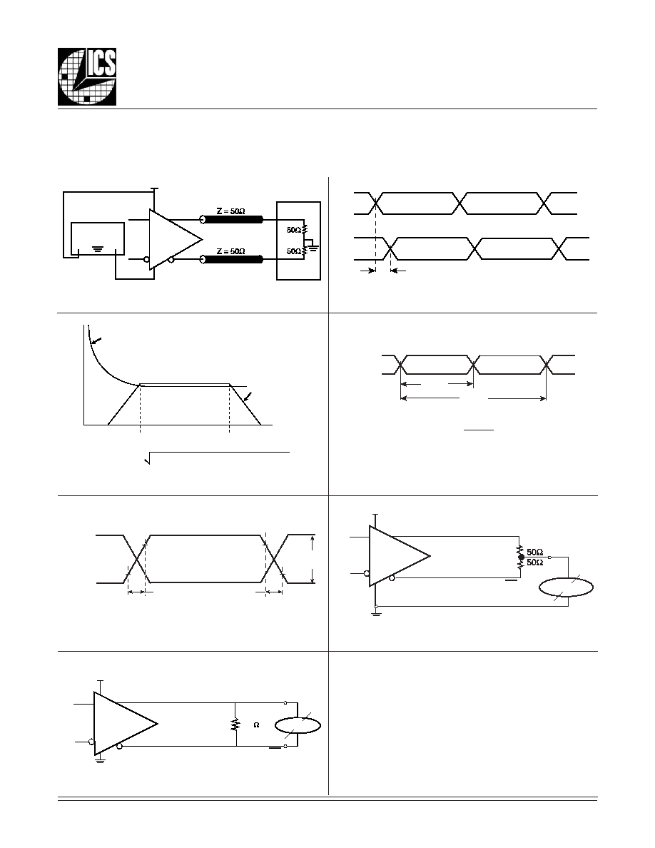
The ICS844004I-04 has been characterized with 18pF
parallel resonant crystals. The capacitor values shown in
Figure 2
below were determined using a 19.44MHz 18pF
parallel resonant crystal and were chosen to minimize
the ppm error.
A
PPLICATION
I
NFORMATION
As in any high speed analog circuitry, the power supply pins
are vulnerable to random noise. The ICS844004I-04 provides
separate power supplies to isolate any high switching
noise from the outputs to the internal PLL. V
DD
, V
DDA
, and V
DDO
should be individually connected to the power supply
plane through vias, and bypass capacitors should be
used for each pin. To achieve optimum jitter performance,
power supply isolation is required.
Figure 1
illustrates how
a 10
resistor along with a 10�F and a .01F bypass
capacitor should be connected to each V
DDA
.
P
OWER
S
UPPLY
F
ILTERING
T
ECHNIQUES
F
IGURE
1. P
OWER
S
UPPLY
F
ILTERING
10
V
DDA
10
F
.01
F
3.3V
.01
F
V
DD
ICS84332
XTAL_IN
XTAL_OUT
X1
18pF Parallel Cry stal
C2
22p
C1
22p
Figure 2. C
RYSTAL
I
NPU
t I
NTERFACE
ICS844004I-04
844004AGI-04
www.icst.com/products/hiperclocks.html
REV. A JANUARY 26, 2006
8
Integrated
Circuit
Systems, Inc.
ICS844004I-04
F
EMTO
C
LOCKS
TM C
RYSTAL
/LVCMOS-
TO
-
LVDS F
REQUENCY
S
YNTHESIZER
PRELIMINARY
3.3V LVDS D
RIVER
T
ERMINATION
A general LVDS interface is shown in
Figure 3.
In a 100
differential transmission line environment, LVDS drivers
require a matched load termination of 100
across near
F
IGURE
3. T
YPICAL
LVDS D
RIVER
T
ERMINATION
the receiver input. For a multiple LVDS outputs buffer, if
only partial outputs are used, it is recommended to termi-
nate the unused outputs.
R1
100
3.3V
100 Ohm Differential Transmission Line
3.3V
+
-
LVDS
I
NPUTS
:
C
RYSTAL
I
NPUT
:
For applications not requiring the use of the crystal oscillator
input, both XTAL_IN and XTAL_OUT can be left floating.
Though not required, but for additional protection, a 1k
resistor can be tied from XTAL_IN to ground.
CLK I
NPUT
:
For applications not requiring the use of a clock input, it can
be left floating. Though not required, but for additional
protection, a 1k
resistor can be tied from the CLK input to
ground.
LVCMOS C
ONTROL
P
INS
:
All control pins have internal pull-ups or pull-downs; additional
resistance is not required but can be added for additional
protection. A 1k
resistor can be used.
R
ECOMMENDATIONS
FOR
U
NUSED
I
NPUT
AND
O
UTPUT
P
INS
O
UTPUTS
:
LVDS
All unused LVDS outputs can be left floating. We recommend
that there is no trace attached. Both sides of the differential
output pair should either be left floating or terminated.
844004AGI-04
www.icst.com/products/hiperclocks.html
REV. A JANUARY 26, 2006
9
Integrated
Circuit
Systems, Inc.
ICS844004I-04
F
EMTO
C
LOCKS
TM C
RYSTAL
/LVCMOS-
TO
-
LVDS F
REQUENCY
S
YNTHESIZER
PRELIMINARY
S
CHEMATIC
E
XAMPLE
Figure 4
shows a schematic example for ICS844004i-04. In this
example, the input is a 19.44MHz parallel resonant crystal with
load capacitor CL=18pF. The 22pF frequency fine tuning
capacitors are used C1 and C2. This example also shows general
logic control input handling. For decoupling capacitors, it is
recommended to have one decouple capacitor per power pin.
C6
0.1u
VCCO
C9
0.1u
RD2
1K
R2
10
+
-
Logic Control Input Examples
Zo = 50 Ohm
Zo = 50 Ohm
RD1
Not Install
C1
27pF
RU1
1K
R3
100
VCC
VCCO
C7
0.1u
VC
C
VCC
RU2
Not Install
X1
19.44MHz
C2
33pF
VCC
To Logic
Input
pins
U1
844004i-04
1
2
3
4
5
6
7
8
9
10
11
12
13
14
15
16
17
18
19
20
21
22
23
24
nQ
1
Q1
VD
D
O
Q0
nQ
0
MR
F
_
SEL3
NC
VD
D
A
F
_
SEL0
VD
D
F
_
SEL1
XT
AL_O
U
T
XT
AL_I
N
GN
D
CL
K
IN
P
U
T
_
S
E
L
F
_
SEL2
GN
D
nQ
3
Q3
VD
D
O
Q2
nQ
2
+
-
Set Logic
Input to
'0'
VCC
C8
0.1u
R4
100
VCCO=3.3V
Zo = 50 Ohm
Set Logic
Input to
'1'
18pF
To Logic
Input
pins
C4
0.01u
VCCA
C3
10uF
VCC=3.3V
Zo = 50 Ohm
F
IGURE
4. ICS844004I-04 S
CHEMATIC
E
XAMPLE
Each decoupling capacitor should be located as close as
possible to the power pin. The low pass filter R2, C3 and C4
should also be located as close to the VCCA pin as possible.
For LVDS driver, the unused output pairs should be terminated
with a 100
resistor across.
844004AGI-04
www.icst.com/products/hiperclocks.html
REV. A JANUARY 26, 2006
10
Integrated
Circuit
Systems, Inc.
ICS844004I-04
F
EMTO
C
LOCKS
TM C
RYSTAL
/LVCMOS-
TO
-
LVDS F
REQUENCY
S
YNTHESIZER
PRELIMINARY
P
OWER
C
ONSIDERATIONS
This section provides information on power dissipation and junction temperature for the ICS844004I-04.
Equations and example calculations are also provided.
1. Power Dissipation.
The total power dissipation for the ICS844004I-04 is the sum of the core power plus the power dissipated in the load(s).
The following is the power dissipation for V
DD
= 3.3V + 5% = 3.465V, which gives worst case results.
�
Power (core)
MAX
= V
DD_MAX
* (I
DD_MAX
+ I
DDA_MAX
) = 3.465V * (80mA + 8mA) = 304.92mW
�
Power (outputs)
MAX
= V
DDO_MAX
* I
DDO_MAX
= 3.465V * 87mA = 301.45mW
Total Power
_MAX
= 304.92mW + 301.45mW = 606.37mW
2. Junction Temperature.
Junction temperature, Tj, is the temperature at the junction of the bond wire and bond pad and directly affects the reliability
of the device. The maximum recommended junction temperature for HiPerClockS
TM
devices is 125�C.
The equation for Tj is as follows: Tj =
JA
* Pd_total + T
A
Tj = Junction Temperature
q
JA
= Junction-to-Ambient Thermal Resistance
Pd_total = Total Device Power Dissipation (example calculation is in section 1 above)
T
A
= Ambient Temperature
In order to calculate junction temperature, the appropriate junction-to-ambient thermal resistance
JA
must be used.
Assuming a moderate air flow of 1 meter per second and a multi-layer board, the appropriate value is 65�C/W per Table 7
below.
Therefore, Tj for an ambient temperature of 85�C with all outputs switching is:
85�C + 0.606W * 65�C/W = 124�C. This is below the limit of 125�C.
This calculation is only an example. Tj will obviously vary depending on the number of loaded outputs, supply voltage, air
flow, and the type of board (single layer or multi-layer).
T
ABLE
7. T
HERMAL
R
ESISTANCE
JA
FOR
24-L
EAD
TSSOP, F
ORCED
C
ONVECTION
JA
by Velocity (Meters per Second)
0
1
2.5
Multi-Layer PCB, JEDEC Standard Test Boards
70�C/W
65�C/W
62�C/W

844004AGI-04
www.icst.com/products/hiperclocks.html
REV. A JANUARY 26, 2006
11
Integrated
Circuit
Systems, Inc.
ICS844004I-04
F
EMTO
C
LOCKS
TM C
RYSTAL
/LVCMOS-
TO
-
LVDS F
REQUENCY
S
YNTHESIZER
PRELIMINARY
R
ELIABILITY
I
NFORMATION
T
RANSISTOR
C
OUNT
The transistor count for ICS844004I-04 is: 2285
T
ABLE
8.
JA
VS
. A
IR
F
LOW
T
ABLE
FOR
24 L
EAD
TSSOP
JA
by Velocity (Meters per Second)
0
1
2.5
Multi-Layer PCB, JEDEC Standard Test Boards
70�C/W
65�C/W
62�C/W

844004AGI-04
www.icst.com/products/hiperclocks.html
REV. A JANUARY 26, 2006
12
Integrated
Circuit
Systems, Inc.
ICS844004I-04
F
EMTO
C
LOCKS
TM C
RYSTAL
/LVCMOS-
TO
-
LVDS F
REQUENCY
S
YNTHESIZER
PRELIMINARY
P
ACKAGE
O
UTLINE
- G S
UFFIX
FOR
24 L
EAD
TSSOP
T
ABLE
9. P
ACKAGE
D
IMENSIONS
Reference Document: JEDEC Publication 95, MO-153
L
O
B
M
Y
S
s
r
e
t
e
m
i
l
l
i
M
m
u
m
i
n
i
M
m
u
m
i
x
a
M
N
4
2
A
-
-
0
2
.
1
1
A
5
0
.
0
5
1
.
0
2
A
0
8
.
0
5
0
.
1
b
9
1
.
0
0
3
.
0
c
9
0
.
0
0
2
.
0
D
0
7
.
7
0
9
.
7
E
C
I
S
A
B
0
4
.
6
1
E
0
3
.
4
0
5
.
4
e
C
I
S
A
B
5
6
.
0
L
5
4
.
0
5
7
.
0
�
0
�
8
a
a
a
-
-
0
1
.
0
844004AGI-04
www.icst.com/products/hiperclocks.html
REV. A JANUARY 26, 2006
13
Integrated
Circuit
Systems, Inc.
ICS844004I-04
F
EMTO
C
LOCKS
TM C
RYSTAL
/LVCMOS-
TO
-
LVDS F
REQUENCY
S
YNTHESIZER
PRELIMINARY
T
ABLE
10. O
RDERING
I
NFORMATION
While the information presented herein has been checked for both accuracy and reliability, Integrated Circuit Systems, Incorporated (ICS) assumes no responsibility for either its use
or for infringement of any patents or other rights of third parties, which would result from its use. No other circuits, patents, or licenses are implied. This product is intended for use
in normal commercial and industrial applications. Any other applications such as those requiring high reliability or other extraordinary environmental requirements are not
recommended without additional processing by ICS. ICS reserves the right to change any circuitry or specifications without notice. ICS does not authorize or warrant any ICS product
for use in life support devices or critical medical instruments.
The aforementioned trademarks, HiPerClockS and F
EMTO
C
LOCKS
are trademarks of Integrated Circuit Systems, Inc. or its subsidiaries in the United States and/or other countries.
r
e
b
m
u
N
r
e
d
r
O
/
t
r
a
P
g
n
i
k
r
a
M
e
g
a
k
c
a
P
g
n
i
g
a
k
c
a
P
g
n
i
p
p
i
h
S
e
r
u
t
a
r
e
p
m
e
T
4
0
-
I
G
A
4
0
0
4
4
8
S
C
I
4
0
I
A
4
0
0
4
4
8
S
C
I
P
O
S
S
T
d
a
e
L
4
2
e
b
u
t
C
�
5
8
o
t
C
�
0
4
-
T
4
0
-
I
G
A
4
0
0
4
4
8
S
C
I
4
0
I
A
4
0
0
4
4
8
S
C
I
P
O
S
S
T
d
a
e
L
4
2
l
e
e
r
&
e
p
a
t
0
0
5
2
C
�
5
8
o
t
C
�
0
4
-
F
L
4
0
-
I
G
A
4
0
0
4
4
8
S
C
I
L
4
0
I
A
4
0
0
4
4
S
C
I
P
O
S
S
T
"
e
e
r
F
-
d
a
e
L
"
d
a
e
L
4
2
e
b
u
t
C
�
5
8
o
t
C
�
0
4
-
T
F
L
4
0
-
I
G
A
4
0
0
4
4
8
S
C
I
L
4
0
I
A
4
0
0
4
4
S
C
I
P
O
S
S
T
"
e
e
r
F
-
d
a
e
L
"
d
a
e
L
4
2
l
e
e
r
&
e
p
a
t
0
0
5
2
C
�
5
8
o
t
C
�
0
4
-
.
t
n
a
il
p
m
o
c
S
H
o
R
e
r
a
d
n
a
n
o
i
t
a
r
u
g
i
f
n
o
c
e
e
r
F
-
b
P
e
h
t
e
r
a
r
e
b
m
u
n
t
r
a
p
e
h
t
o
t
x
i
f
f
u
s
"
F
L
"
n
a
h
t
i
w
d
e
r
e
d
r
o
e
r
a
t
a
h
t
s
t
r
a
P
:
E
T
O
N