Document Outline
- General Description
- Features
- Common Configuration Table
- Block Diagram
- Pin Assignment
- Pin Descriptions
- Pin Characteristics
- Absolute Maximum Ratings
- 3.3V Power Supply DC Characteristics
- 2.5V Power Supply DC Characteristics
- LVCMOS DC Characteristics
- 3.3V LVDS DC Characteristics
- 2.5V LVDS DC Characteristics
- Crystal Characteristics
- 3.3V AC Characteristics
- 2.5V AC Characteristics
- Parameter Measurement Information
- LVDS 3.3V Output Load AC Test Circuit Diagram
- LVDS 2.5V Output Load AC Test Circuit Diagram
- Output Rise/Fall Time Diagram
- Output Duty Cycle/Pulse Width/Period Diagram
- RMS Phase Jitter Diagram
- Offset Voltage Setup Diagram
- Differential Output Voltage Setup Diagram
- Application Information
- Power Supply Filtering Techniques
- Crystal Input Interface
- LVDS Driver Termination
- Reliability Information
- Transistor Count
- Package Outline
- Package Dimensions
- Ordering Information
844021AGI-01
www.icst.com/products/hiperclocks.html
REV. A MARCH 29, 2005
1
Integrated
Circuit
Systems, Inc.
ICS844021I-01
F
EMTO
C
LOCKS
TM C
RYSTAL
-
TO
- LVDS
C
LOCK
G
ENERATOR
PRELIMINARY
G
ENERAL
D
ESCRIPTION
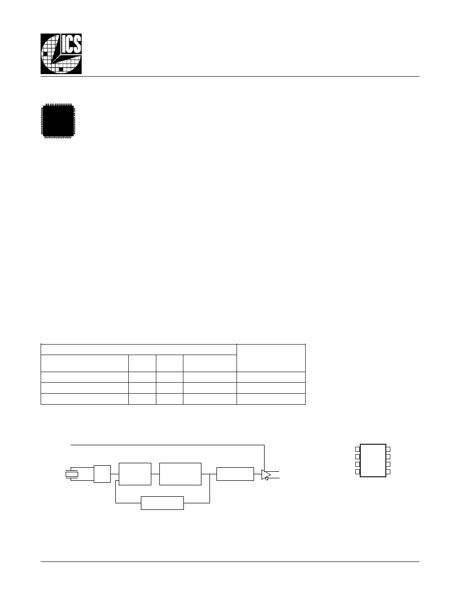
The ICS844021I-01 is an Ethernet Clock
Generator and a member of the HiPerClocks
TM
family of high performance devices from ICS. The
ICS844021I-01 uses an 18pF parallel resonant
crystal over the range of 24.5MHz - 34MHz. For
Ether net applications, a 25MHz cr ystal is used. The
ICS844021I-01 has excellent <1ps phase jitter performance,
over the 1.875MHz - 20MHz integration range. The
ICS844021I-01 is packaged in a small 8-pin TSSOP, making
it ideal for use in systems with limited board space.
F
EATURES
∑ (1) Differential LVDS output
∑ Crystal oscillator interface, 18pF parallel resonant crystal
(24.5MHz - 34MHz)
∑ Output frequency range: 122.5MHz - 170MHz
∑ VCO range: 490MHz - 680MHz
∑ RMS phase jitter @ 125MHz, using a 25MHz crystal
(1.875MHz - 20MHz): 0.45ps (typical)
∑ 3.3V or 2.5V operating supply
∑ -40∞C to 85∞C ambient operating temperature
HiPerClockSTM
ICS
ICS844021I-01
8-Lead TSSOP
4.40mm x 3.0mm x 0.925mm
package body
G Package
Top View
V
DDA
GND
XTAL_OUT
XTAL_IN
1
2
3
4
V
DD
Q0
nQ0
OE
8
7
6
5
B
LOCK
D
IAGRAM
OSC
Phase
Detector
VCO
490MHz - 680MHz
M = ˜20
(fixed)
N = ˜4
(fixed)
XTAL_IN
XTAL_OUT
Q0
nQ0
C
OMMON
C
ONFIGURATION
T
ABLE
- Gb E
THERNET
P
IN
A
SSIGNMENT
OE
s
t
u
p
n
I
y
c
n
e
u
q
e
r
F
t
u
p
t
u
O
)
z
H
M
(
)
z
H
M
(
y
c
n
e
u
q
e
r
F
l
a
t
s
y
r
C
M
N
n
o
i
t
a
c
i
l
p
i
t
l
u
M
N
/
M
e
u
l
a
V
5
2
0
2
4
5
5
2
1
6
6
6
.
6
2
0
2
4
5
3
3
.
3
3
1
3
3
.
3
3
0
2
4
5
6
6
.
6
6
1
Pullup
The Preliminary Information presented herein represents a product in prototyping or pre-production. The noted characteristics are based on initial
product characterization. Integrated Circuit Systems, Incorporated (ICS) reserves the right to change any circuitry or specifications without notice.
844021AGI-01
www.icst.com/products/hiperclocks.html
REV. A MARCH 29, 2005
2
Integrated
Circuit
Systems, Inc.
ICS844021I-01
F
EMTO
C
LOCKS
TM C
RYSTAL
-
TO
- LVDS
C
LOCK
G
ENERATOR
PRELIMINARY
T
ABLE
2. P
IN
C
HARACTERISTICS
T
ABLE
1. P
IN
D
ESCRIPTIONS
r
e
b
m
u
N
e
m
a
N
e
p
y
T
n
o
i
t
p
i
r
c
s
e
D
1
V
A
D
D
r
e
w
o
P
.
n
i
p
y
l
p
p
u
s
g
o
l
a
n
A
2
D
N
G
r
e
w
o
P
.
d
n
u
o
r
g
y
l
p
p
u
s
r
e
w
o
P
4
,
3
,
T
U
O
_
L
A
T
X
N
I
_
L
A
T
X
t
u
p
n
I
,
t
u
p
n
i
e
h
t
s
i
N
I
_
L
A
T
X
.
e
c
a
f
r
e
t
n
i
r
o
t
a
ll
i
c
s
o
l
a
t
s
y
r
C
.
t
u
p
t
u
o
e
h
t
s
i
T
U
O
_
L
A
T
X
5
E
O
t
u
p
n
I
p
u
ll
u
P
.
e
v
i
t
c
a
s
i
t
u
p
t
u
o
0
Q
n
/
0
Q
,
H
G
I
H
n
e
h
W
.
n
i
p
e
l
b
a
n
e
t
u
p
t
u
O
.
e
t
a
t
s
e
c
n
a
d
e
p
m
i
h
g
i
h
a
n
i
s
i
t
u
p
t
u
o
0
Q
n
/
0
Q
e
h
t
,
W
O
L
n
e
h
W
.
s
l
e
v
e
l
e
c
a
f
r
e
t
n
i
L
T
T
V
L
/
S
O
M
C
V
L
7
,
6
0
Q
,
0
Q
n
t
u
p
t
u
O
.
s
l
e
v
e
l
e
c
a
f
r
e
t
n
i
S
D
V
L
.
s
t
u
p
t
u
o
k
c
o
l
c
l
a
i
t
n
e
r
e
f
f
i
D
8
V
D
D
r
e
w
o
P
.
n
i
p
y
l
p
p
u
s
e
r
o
C
:
E
T
O
N
p
u
ll
u
P
.
s
e
u
l
a
v
l
a
c
i
p
y
t
r
o
f
,
s
c
i
t
s
i
r
e
t
c
a
r
a
h
C
n
i
P
,
2
e
l
b
a
T
e
e
S
.
s
r
o
t
s
i
s
e
r
t
u
p
n
i
l
a
n
r
e
t
n
i
o
t
s
r
e
f
e
r
l
o
b
m
y
S
r
e
t
e
m
a
r
a
P
s
n
o
i
t
i
d
n
o
C
t
s
e
T
m
u
m
i
n
i
M
l
a
c
i
p
y
T
m
u
m
i
x
a
M
s
t
i
n
U
C
N
I
e
c
n
a
t
i
c
a
p
a
C
t
u
p
n
I
4
F
p
R
P
U
L
L
U
P
r
o
t
s
i
s
e
R
p
u
ll
u
P
t
u
p
n
I
1
5
k
844021AGI-01
www.icst.com/products/hiperclocks.html
REV. A MARCH 29, 2005
3
Integrated
Circuit
Systems, Inc.
ICS844021I-01
F
EMTO
C
LOCKS
TM C
RYSTAL
-
TO
- LVDS
C
LOCK
G
ENERATOR
PRELIMINARY
T
ABLE
3A. P
OWER
S
UPPLY
DC C
HARACTERISTICS
,
V
DD
= V
DDA
= 3.3V±5%, T
A
= -40∞C
TO
85∞C
l
o
b
m
y
S
r
e
t
e
m
a
r
a
P
s
n
o
i
t
i
d
n
o
C
t
s
e
T
m
u
m
i
n
i
M
l
a
c
i
p
y
T
m
u
m
i
x
a
M
s
t
i
n
U
V
D
D
e
g
a
t
l
o
V
y
l
p
p
u
S
e
r
o
C
5
3
1
.
3
3
.
3
5
6
4
.
3
V
V
A
D
D
e
g
a
t
l
o
V
y
l
p
p
u
S
g
o
l
a
n
A
5
3
1
.
3
3
.
3
5
6
4
.
3
V
I
D
D
t
n
e
r
r
u
C
y
l
p
p
u
S
r
e
w
o
P
D
B
T
A
m
I
A
D
D
t
n
e
r
r
u
C
y
l
p
p
u
S
g
o
l
a
n
A
D
B
T
A
m
A
BSOLUTE
M
AXIMUM
R
ATINGS
Supply Voltage, V
DD
4.6V
Inputs, V
I
-0.5V to V
DD
+ 0.5 V
Outputs, I
O
(LVDS)
Continuous Current
10mA
Surge Current
15mA
Package Thermal Impedance,
JA
101.7∞C/W (0 mps)
Storage Temperature, T
STG
-65∞C to 150∞C
NOTE: Stresses beyond those listed under Absolute
Maximum Ratings may cause permanent damage to the
device. These ratings are stress specifications only. Functional
operation of product at these conditions or any conditions be-
yond those listed in the
DC Characteristics or AC Character-
istics is not implied. Exposure to absolute maximum rating
conditions for extended periods may affect product reliability.
T
ABLE
3C. LVCMOS/LVTTL DC C
HARACTERISTICS
,
V
DD
= V
DDA
= 3.3V±5%
OR
2.5V±5%, T
A
= -40∞C
TO
85∞C
l
o
b
m
y
S
r
e
t
e
m
a
r
a
P
s
n
o
i
t
i
d
n
o
C
t
s
e
T
m
u
m
i
n
i
M
l
a
c
i
p
y
T
m
u
m
i
x
a
M
s
t
i
n
U
V
H
I
e
g
a
t
l
o
V
h
g
i
H
t
u
p
n
I
V
D
D
V
3
.
3
=
2
V
D
D
3
.
0
+
V
V
D
D
V
5
.
2
=
7
.
1
V
D
D
3
.
0
+
V
V
L
I
e
g
a
t
l
o
V
w
o
L
t
u
p
n
I
V
D
D
V
3
.
3
=
3
.
0
-
8
.
0
V
V
D
D
V
5
.
2
=
3
.
0
-
7
.
0
V
I
H
I
t
n
e
r
r
u
C
h
g
i
H
t
u
p
n
I
E
O
V
D
D
V
=
N
I
V
5
2
6
.
2
r
o
V
5
6
4
.
3
=
5
A
µ
I
L
I
t
n
e
r
r
u
C
w
o
L
t
u
p
n
I
E
O
V
D
D
V
,
V
5
2
6
.
2
r
o
V
5
6
4
.
3
=
N
I
V
0
=
0
5
1
-
A
µ
T
ABLE
3B. P
OWER
S
UPPLY
DC C
HARACTERISTICS
,
V
DD
= V
DDA
= 2.5V±5%, T
A
= -40∞C
TO
85∞C
l
o
b
m
y
S
r
e
t
e
m
a
r
a
P
s
n
o
i
t
i
d
n
o
C
t
s
e
T
m
u
m
i
n
i
M
l
a
c
i
p
y
T
m
u
m
i
x
a
M
s
t
i
n
U
V
D
D
e
g
a
t
l
o
V
y
l
p
p
u
S
e
r
o
C
5
7
3
.
2
5
.
2
5
2
6
.
2
V
V
A
D
D
e
g
a
t
l
o
V
y
l
p
p
u
S
g
o
l
a
n
A
5
7
3
.
2
5
.
2
5
2
6
.
2
V
I
D
D
t
n
e
r
r
u
C
y
l
p
p
u
S
r
e
w
o
P
D
B
T
A
m
I
A
D
D
t
n
e
r
r
u
C
y
l
p
p
u
S
g
o
l
a
n
A
D
B
T
A
m
844021AGI-01
www.icst.com/products/hiperclocks.html
REV. A MARCH 29, 2005
4
Integrated
Circuit
Systems, Inc.
ICS844021I-01
F
EMTO
C
LOCKS
TM C
RYSTAL
-
TO
- LVDS
C
LOCK
G
ENERATOR
PRELIMINARY
T
ABLE
4. C
RYSTAL
C
HARACTERISTICS
r
e
t
e
m
a
r
a
P
s
n
o
i
t
i
d
n
o
C
t
s
e
T
m
u
m
i
n
i
M
l
a
c
i
p
y
T
m
u
m
i
x
a
M
s
t
i
n
U
n
o
i
t
a
ll
i
c
s
O
f
o
e
d
o
M
l
a
t
n
e
m
a
d
n
u
F
y
c
n
e
u
q
e
r
F
5
.
4
2
4
3
z
H
M
)
R
S
E
(
e
c
n
a
t
s
i
s
e
R
s
e
i
r
e
S
t
n
e
l
a
v
i
u
q
E
0
5
e
c
n
a
t
i
c
a
p
a
C
t
n
u
h
S
7
F
p
l
e
v
e
L
e
v
i
r
D
1
W
m
T
ABLE
5A. AC C
HARACTERISTICS
,
V
DD
= V
DDA
= 3.3V±5%, T
A
= -40∞C
TO
85∞C
l
o
b
m
y
S
r
e
t
e
m
a
r
a
P
s
n
o
i
t
i
d
n
o
C
t
s
e
T
m
u
m
i
n
i
M
l
a
c
i
p
y
T
m
u
m
i
x
a
M
s
t
i
n
U
f
T
U
O
y
c
n
e
u
q
e
r
F
t
u
p
t
u
O
5
.
2
2
1
0
7
1
z
H
M
t
)
ÿ
(
t
ij
;
)
m
o
d
n
a
R
(
r
e
t
t
i
J
e
s
a
h
P
S
M
R
1
E
T
O
N
:
e
g
n
a
R
n
o
i
t
a
r
g
e
t
n
I
@
z
H
M
5
2
1
z
H
M
0
2
-
z
H
M
5
7
8
.
1
5
4
.
0
s
p
:
e
g
n
a
R
n
o
i
t
a
r
g
e
t
n
I
@
z
H
M
3
3
.
3
3
1
z
H
M
0
2
-
z
H
M
5
7
8
.
1
D
B
T
s
p
:
e
g
n
a
R
n
o
i
t
a
r
g
e
t
n
I
@
z
H
M
6
6
.
6
6
1
z
H
M
0
2
-
z
H
M
5
7
8
.
1
D
B
T
s
p
t
R
t
/
F
e
m
i
T
ll
a
F
/
e
s
i
R
t
u
p
t
u
O
%
0
8
o
t
%
0
2
0
0
3
s
p
c
d
o
e
l
c
y
C
y
t
u
D
t
u
p
t
u
O
0
5
%
.
n
o
i
t
c
e
s
s
i
h
t
g
n
i
w
o
ll
o
f
s
t
o
l
P
e
s
i
o
N
e
s
a
h
P
e
h
t
o
t
r
e
f
e
r
e
s
a
e
l
P
:
1
E
T
O
N
T
ABLE
5B. AC C
HARACTERISTICS
,
V
DD
= V
DDA
= 2.5V±5%, T
A
= -40∞C
TO
85∞C
l
o
b
m
y
S
r
e
t
e
m
a
r
a
P
s
n
o
i
t
i
d
n
o
C
t
s
e
T
m
u
m
i
n
i
M
l
a
c
i
p
y
T
m
u
m
i
x
a
M
s
t
i
n
U
f
T
U
O
y
c
n
e
u
q
e
r
F
t
u
p
t
u
O
5
.
2
2
1
0
7
1
z
H
M
t
)
ÿ
(
t
ij
;
)
m
o
d
n
a
R
(
r
e
t
t
i
J
e
s
a
h
P
S
M
R
1
E
T
O
N
:
e
g
n
a
R
n
o
i
t
a
r
g
e
t
n
I
@
z
H
M
5
2
1
z
H
M
0
2
-
z
H
M
5
7
8
.
1
5
4
.
0
s
p
:
e
g
n
a
R
n
o
i
t
a
r
g
e
t
n
I
@
z
H
M
3
3
.
3
3
1
z
H
M
0
2
-
z
H
M
5
7
8
.
1
D
B
T
s
p
:
e
g
n
a
R
n
o
i
t
a
r
g
e
t
n
I
@
z
H
M
6
6
.
6
6
1
z
H
M
0
2
-
z
H
M
5
7
8
.
1
D
B
T
s
p
t
R
t
/
F
e
m
i
T
ll
a
F
/
e
s
i
R
t
u
p
t
u
O
%
0
8
o
t
%
0
2
0
2
3
s
p
c
d
o
e
l
c
y
C
y
t
u
D
t
u
p
t
u
O
0
5
%
.
n
o
i
t
c
e
s
s
i
h
t
g
n
i
w
o
ll
o
f
s
t
o
l
P
e
s
i
o
N
e
s
a
h
P
e
h
t
o
t
r
e
f
e
r
e
s
a
e
l
P
:
1
E
T
O
N
T
ABLE
3E. LVDS DC C
HARACTERISTICS
,
V
DD
= V
DDA
= 2.5V±5%, T
A
= -40∞C
TO
85∞C
l
o
b
m
y
S
r
e
t
e
m
a
r
a
P
s
n
o
i
t
i
d
n
o
C
t
s
e
T
m
u
m
i
n
i
M
l
a
c
i
p
y
T
m
u
m
i
x
a
M
s
t
i
n
U
V
D
O
e
g
a
t
l
o
V
t
u
p
t
u
O
l
a
i
t
n
e
r
e
f
f
i
D
0
0
4
V
m
V
D
O
V
D
O
e
g
n
a
h
C
e
d
u
t
i
n
g
a
M
0
4
V
m
V
S
O
e
g
a
t
l
o
V
t
e
s
f
f
O
2
.
1
V
V
S
O
V
S
O
e
g
n
a
h
C
e
d
u
t
i
n
g
a
M
0
5
V
m
.
n
o
i
t
a
m
r
o
f
n
i
t
u
p
t
u
o
r
o
f
n
o
i
t
a
m
r
o
f
n
I
t
n
e
m
e
r
u
s
a
e
M
r
e
t
e
m
a
r
a
P
o
t
r
e
f
e
r
e
s
a
e
l
P
:
E
T
O
N
T
ABLE
3D. LVDS DC C
HARACTERISTICS
,
V
DD
= V
DDA
= 3.3V±5%, T
A
= -40∞C
TO
85∞C
l
o
b
m
y
S
r
e
t
e
m
a
r
a
P
s
n
o
i
t
i
d
n
o
C
t
s
e
T
m
u
m
i
n
i
M
l
a
c
i
p
y
T
m
u
m
i
x
a
M
s
t
i
n
U
V
D
O
e
g
a
t
l
o
V
t
u
p
t
u
O
l
a
i
t
n
e
r
e
f
f
i
D
0
0
4
V
m
V
D
O
V
D
O
e
g
n
a
h
C
e
d
u
t
i
n
g
a
M
0
4
V
m
V
S
O
e
g
a
t
l
o
V
t
e
s
f
f
O
3
.
1
V
V
S
O
V
S
O
e
g
n
a
h
C
e
d
u
t
i
n
g
a
M
0
5
V
m
.
n
o
i
t
a
m
r
o
f
n
i
t
u
p
t
u
o
r
o
f
n
o
i
t
a
m
r
o
f
n
I
t
n
e
m
e
r
u
s
a
e
M
r
e
t
e
m
a
r
a
P
o
t
r
e
f
e
r
e
s
a
e
l
P
:
E
T
O
N
844021AGI-01
www.icst.com/products/hiperclocks.html
REV. A MARCH 29, 2005
5
Integrated
Circuit
Systems, Inc.
ICS844021I-01
F
EMTO
C
LOCKS
TM C
RYSTAL
-
TO
- LVDS
C
LOCK
G
ENERATOR
PRELIMINARY
P
ARAMETER
M
EASUREMENT
I
NFORMATION
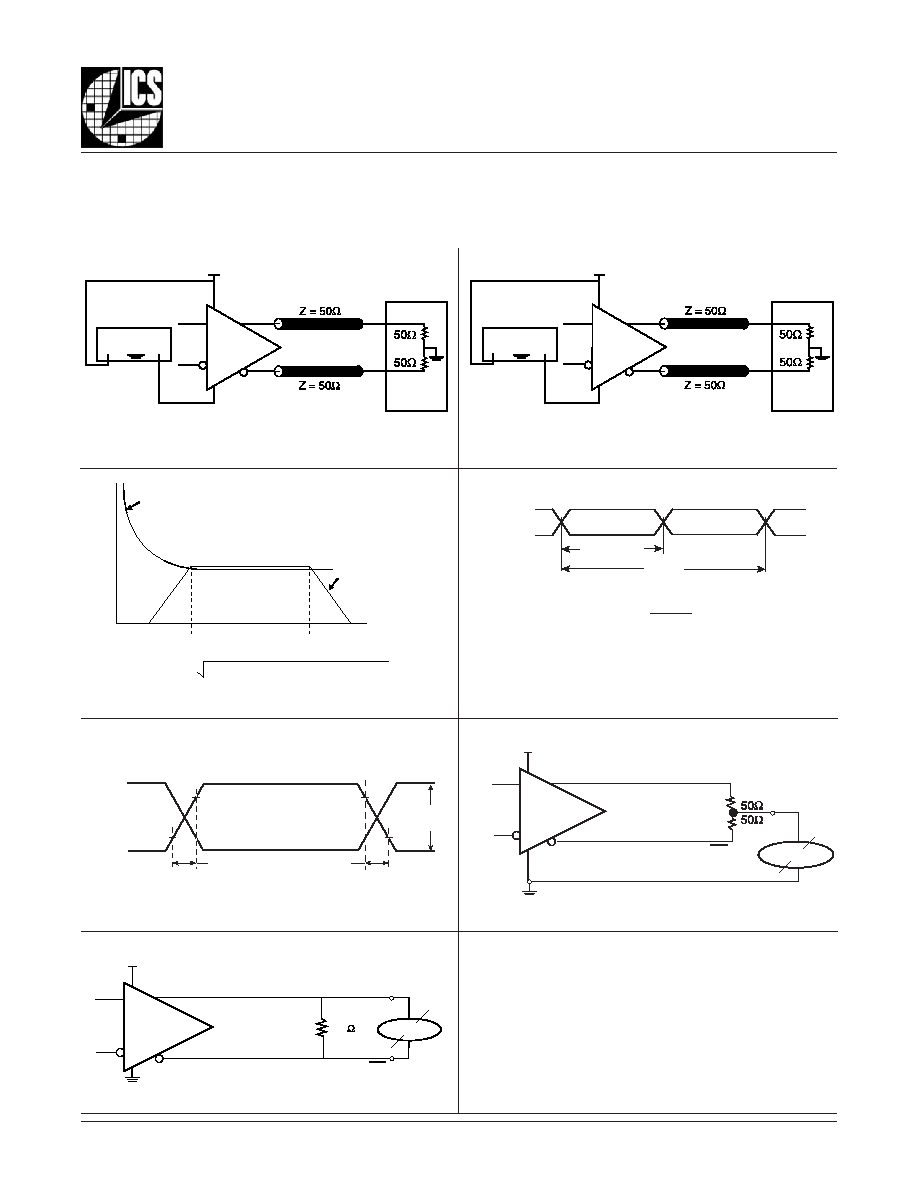
O
UTPUT
R
ISE
/F
ALL
T
IME
O
FFSET
V
OLTAGE
S
ETUP
LVDS 3.3V O
UTPUT
L
OAD
AC T
EST
C
IRCUIT
LVDS 2.5V O
UTPUT
L
OAD
AC T
EST
C
IRCUIT
RMS P
HASE
J
ITTER
O
UTPUT
D
UTY
C
YCLE
/P
ULSE
W
IDTH
/P
ERIOD
SCOPE
Qx
nQx
LVDS
3.3V±5%
POWER SUPPLY
+
-
Float GND
Q0
nQ0
100
out
out
LVDS
DC Input
V
OD
/
V
OD
V
DD
out
out
LVDS
DC Input
V
OS
/
V
OS
V
DD
V
DD
V
DD
Clock
Outputs
20%
80%
80%
20%
t
R
t
F
V
SW I N G
D
IFFERENTIAL
O
UTPUT
V
OLTAGE
S
ETUP
SCOPE
Qx
nQx
LVDS
2.5V±5%
POWER SUPPLY
+
-
Float GND
Phase Noise Mask
Offset Frequency
f
1
f
2
Phase Noise Plot
RMS Jitter = Area Under the Masked Phase Noise Plot
Noise P
o
w
er
Pulse Width
t
PERIOD
t
PW
t
PERIOD
odc =

844021AGI-01
www.icst.com/products/hiperclocks.html
REV. A MARCH 29, 2005
6
Integrated
Circuit
Systems, Inc.
ICS844021I-01
F
EMTO
C
LOCKS
TM C
RYSTAL
-
TO
- LVDS
C
LOCK
G
ENERATOR
PRELIMINARY
A
PPLICATION
I
NFORMATION
Figure 2. C
RYSTAL
I
NPU
t I
NTERFACE
C
RYSTAL
I
NPUT
I
NTERFACE
The ICS844021I-01 has been characterized with 18pF parallel
resonant crystals. The capacitor values, C1 and C2, shown in
Figure 2 below were determined using a 25MHz, 18pF parallel
resonant crystal and were chosen to minimize the ppm error.
The optimum C1 and C2 values can be slightly adjusted for dif-
ferent board layouts.
C1
33p
X1
18pF Parallel Crystal
C2
27p
XTAL_OUT
XTAL_IN
P
OWER
S
UPPLY
F
ILTERING
T
ECHNIQUES
As in any high speed analog circuitry, the power supply pins
are vulnerable to random noise. The ICS844021I-01 provides
separate power supplies to isolate any high switching
noise from the outputs to the internal PLL. V
DD
and V
DDA
should
b e i n d i v i d u a l l y c o n n e c t e d t o t h e p o w e r s u p p l y
plane through vias, and bypass capacitors should be
used for each pin. To achieve optimum jitter performance,
power supply isolation is required.
Figure 1 illustrates how
a 10
resistor along with a 10F and a .01F bypass
capacitor should be connected to each V
DDA
pin.
F
IGURE
1. P
OWER
S
UPPLY
F
ILTERING
10
V
DDA
10
F
.01
F
3.3V or 2.5V
.01
F
V
DD
844021AGI-01
www.icst.com/products/hiperclocks.html
REV. A MARCH 29, 2005
7
Integrated
Circuit
Systems, Inc.
ICS844021I-01
F
EMTO
C
LOCKS
TM C
RYSTAL
-
TO
- LVDS
C
LOCK
G
ENERATOR
PRELIMINARY
3.3V, 2.5V LVDS D
RIVER
T
ERMINATION
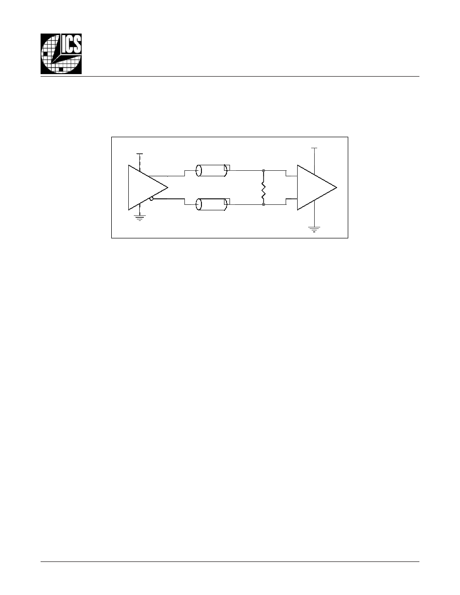
A general LVDS interface is shown in
Figure 3. In a 100
differential transmission line environment, LVDS drivers
require a matched load termination of 100
across near
F
IGURE
3. T
YPICAL
LVDS D
RIVER
T
ERMINATION
the receiver input. For a multiple LVDS outputs buffer, if only
partial outputs are used, it is recommended to terminate the
un-used outputs.
R1
100
3.3V or 2.5V
100
Differential Transmission
VDD
+
-
LVDS
844021AGI-01
www.icst.com/products/hiperclocks.html
REV. A MARCH 29, 2005
8
Integrated
Circuit
Systems, Inc.
ICS844021I-01
F
EMTO
C
LOCKS
TM C
RYSTAL
-
TO
- LVDS
C
LOCK
G
ENERATOR
PRELIMINARY
R
ELIABILITY
I
NFORMATION
T
RANSISTOR
C
OUNT
The transistor count for ICS844021I-01 is: 2533
T
ABLE
6.
JA
VS
. A
IR
F
LOW
T
ABLE
FOR
8 L
EAD
TSSOP
JA
by Velocity (Meters per Second)
0
1
2.5
Multi-Layer PCB, JEDEC Standard Test Boards
101.7∞C/W
90.5∞C/W
89.8∞C/W
844021AGI-01
www.icst.com/products/hiperclocks.html
REV. A MARCH 29, 2005
9
Integrated
Circuit
Systems, Inc.
ICS844021I-01
F
EMTO
C
LOCKS
TM C
RYSTAL
-
TO
- LVDS
C
LOCK
G
ENERATOR
PRELIMINARY
P
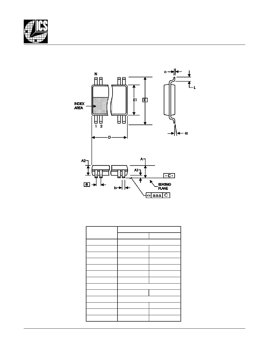
ACKAGE
O
UTLINE
- G S
UFFIX
FOR
8 L
EAD
TSSOP
T
ABLE
7. P
ACKAGE
D
IMENSIONS
Reference Document: JEDEC Publication 95, MO-153
L
O
B
M
Y
S
s
r
e
t
e
m
i
l
l
i
M
m
u
m
i
n
i
M
m
u
m
i
x
a
M
N
8
A
-
-
0
2
.
1
1
A
5
0
.
0
5
1
.
0
2
A
0
8
.
0
5
0
.
1
b
9
1
.
0
0
3
.
0
c
9
0
.
0
0
2
.
0
D
0
9
.
2
0
1
.
3
E
C
I
S
A
B
0
4
.
6
1
E
0
3
.
4
0
5
.
4
e
C
I
S
A
B
5
6
.
0
L
5
4
.
0
5
7
.
0
∞
0
∞
8
a
a
a
-
-
0
1
.
0
844021AGI-01
www.icst.com/products/hiperclocks.html
REV. A MARCH 29, 2005
10
Integrated
Circuit
Systems, Inc.
ICS844021I-01
F
EMTO
C
LOCKS
TM C
RYSTAL
-
TO
- LVDS
C
LOCK
G
ENERATOR
PRELIMINARY
T
ABLE
8. O
RDERING
I
NFORMATION
While the information presented herein has been checked for both accuracy and reliability, Integrated Circuit Systems, Incorporated (ICS) assumes no responsibility for either its use
or for infringement of any patents or other rights of third parties, which would result from its use. No other circuits, patents, or licenses are implied. This product is intended for use
in normal commercial and industrial applications. Any other applications such as those requiring high reliability or other extraordinary environmental requirements are not
recommended without additional processing by ICS. ICS reserves the right to change any circuitry or specifications without notice. ICS does not authorize or warrant any ICS product
for use in life support devices or critical medical instruments.
r
e
b
m
u
N
r
e
d
r
O
/
t
r
a
P
g
n
i
k
r
a
M
e
g
a
k
c
a
P
g
n
i
g
a
k
c
a
P
g
n
i
p
p
i
h
S
e
r
u
t
a
r
e
p
m
e
T
1
0
-
I
G
A
1
2
0
4
4
8
S
C
I
1
0
I
A
1
P
O
S
S
T
d
a
e
l
8
e
b
u
t
C
∞
5
8
o
t
C
∞
0
4
-
T
1
0
-
I
G
A
1
2
0
4
4
8
S
C
I
1
0
I
A
1
P
O
S
S
T
d
a
e
l
8
l
e
e
r
&
e
p
a
t
0
0
5
2
C
∞
5
8
o
t
C
∞
0
4
-
The aforementioned trademarks, HiPerClockSTM and FemtoClocksTM are a trademark of Integrated Circuit Systems, Inc. or its subsidiaries in the United States and/or other countries.