Document Outline
- General Description
- Features
- Block Diagram
- Pin Assignment
- Pin Descriptions
- Pin Characteristics
- Absolute Maximum Ratings
- Power Supply DC Characteristics
- LVCMOS DC Characteristics
- LVDS DC Characteristics
- Crystal Characteristics
- AC Characteristics
- Typical Phase Noise Plots
- Parameter Measurement Information
- Application Information
- Power Supply Filtering Techniques
- Crystal Input Interface
- LVDS Driver Termination
- Recommendations for Unused Output Pins
- Schematic Example
- Power & Grounding
- Clock Traces & Termination
- Crystal
- PCB Board Layout
- Reliability Information
- Transistor Count
- Package Outline
- Package Dimensions
- Ordering Information
84427CM
www.icst.com/products/hiperclocks.html
REV. D NOVEMBER 30, 2005
1
Integrated
Circuit
Systems, Inc.
ICS84427
C
RYSTAL
-
TO
-LVDS
I
NTEGRATED
F
REQUENCY
S
YNTHESIZER
/F
ANOUT
B
UFFER
PRELIMINARY
G
ENERAL
D
ESCRIPTION
The ICS84427 is a Crystal-to-LVDS Frequency
Synthesizer/Fanout Buffer and a member of the
HiPerClockSTM family of High Performance Clock
Solutions from ICS. The output frequency can be
programmed using the frequency select pins. The
low phase noise characteristics of the ICS84427 make it an
ideal clock source for 10 Gigabit Ethernet, 10 Gigabit Fibre
Channel, OC3 and OC12 applications.
B
LOCK
D
IAGRAM
P
IN
A
SSIGNMENT
F
EATURES
� Six LVDS outputs
� Crystal oscillator interface
� Output frequency range: 77.76MHz to 625MHz
� Crystal input frequency: 19.44MHz, 25MHz or 25.5MHz
� RMS phase jitter at 155.52MHz, using a 19.44MHz crystal
(12kHz to 20MHz): 3.4ps (typical)
Phase noise:
Offset
Noise Power
100Hz ................. -95 dBc/Hz
1kHz ............... -110 dBc/Hz
10kHz ............... -120 dBc/Hz
100kHz ............... -121 dBc/Hz
� 3.3V supply voltage
� 0�C to 70�C ambient operating temperature
� Industrial temperature information available upon request
� Available in both standard and lead-free RoHS-compliant
packages
HiPerClockSTM
ICS
Q0:Q5
ICS84427
24-Lead, 300-MIL SOIC
7.5mm x 15.33mm x 2.3mm body package
M Package
Top View
Q0
nQ0
Q1
nQ1
Q2
nQ2
Q3
nQ3
Q4
nQ4
Q5
nQ5
1
2
3
4
5
6
7
8
9
10
11
12
V
DD
F_SEL0
F_SEL1
MR
XTAL_IN
XTAL_OUT
F_SEL2
V
DDA
V
DD
PLL_SEL
GND
V
DD
PLL
6
/
Feedback
Divider
OSC
6
/
Output
Divider
0
1
XTAL_IN
XTAL_OUT
F_SEL2
PLL_SEL
MR
F_SEL0
nQ0:nQ5
24
23
22
21
20
19
18
17
16
15
14
13
F_SEL1
F
UNCTION
T
ABLE
s
t
u
p
n
I
t
u
p
t
u
O
y
c
n
e
u
q
e
r
F
L
A
T
X
_
F
R
M
2
L
E
S
_
F
1
L
E
S
_
F
0
L
E
S
_
F
T
U
O
_
F
X
1
X
X
X
W
O
L
z
H
M
4
4
.
9
1
0
1
0
0
z
H
M
6
7
.
7
7
z
H
M
4
4
.
9
1
0
1
0
1
z
H
M
2
5
.
5
5
1
z
H
M
4
4
.
9
1
0
1
1
0
z
H
M
4
0
.
1
1
3
z
H
M
4
4
.
9
1
0
1
1
1
z
H
M
8
0
.
2
2
6
z
H
M
5
2
0
0
0
0
z
H
M
5
2
1
.
8
7
z
H
M
5
2
0
0
0
1
z
H
M
5
2
.
6
5
1
z
H
M
5
2
0
0
1
0
z
H
M
5
.
2
1
3
z
H
M
5
2
0
0
1
1
z
H
M
5
2
6
z
H
M
5
.
5
2
0
0
0
1
z
H
M
5
7
3
.
9
5
1
The Preliminary Information presented herein represents a product in prototyping or pre-production. The noted characteristics are based on initial
product characterization. Integrated Circuit Systems, Incorporated (ICS) reserves the right to change any circuitry or specifications without notice.

84427CM
www.icst.com/products/hiperclocks.html
REV. D NOVEMBER 30, 2005
2
Integrated
Circuit
Systems, Inc.
ICS84427
C
RYSTAL
-
TO
-LVDS
I
NTEGRATED
F
REQUENCY
S
YNTHESIZER
/F
ANOUT
B
UFFER
PRELIMINARY
T
ABLE
1. P
IN
D
ESCRIPTIONS
T
ABLE
2. P
IN
C
HARACTERISTICS
l
o
b
m
y
S
r
e
t
e
m
a
r
a
P
s
n
o
i
t
i
d
n
o
C
t
s
e
T
m
u
m
i
n
i
M
l
a
c
i
p
y
T
m
u
m
i
x
a
M
s
t
i
n
U
C
N
I
e
c
n
a
t
i
c
a
p
a
C
t
u
p
n
I
4
F
p
R
P
U
L
L
U
P
r
o
t
s
i
s
e
R
p
u
ll
u
P
t
u
p
n
I
1
5
k
R
N
W
O
D
L
L
U
P
r
o
t
s
i
s
e
R
n
w
o
d
ll
u
P
t
u
p
n
I
1
5
k
r
e
b
m
u
N
e
m
a
N
e
p
y
T
n
o
i
t
p
i
r
c
s
e
D
2
,
1
0
Q
n
,
0
Q
t
u
p
t
u
O
.
s
l
e
v
e
l
e
c
a
f
r
e
t
n
i
S
D
V
L
.
r
i
a
p
t
u
p
t
u
o
l
a
i
t
n
e
r
e
f
f
i
D
4
,
3
1
Q
n
,
1
Q
t
u
p
t
u
O
.
s
l
e
v
e
l
e
c
a
f
r
e
t
n
i
S
D
V
L
.
r
i
a
p
t
u
p
t
u
o
l
a
i
t
n
e
r
e
f
f
i
D
6
,
5
2
Q
n
,
2
Q
t
u
p
t
u
O
.
s
l
e
v
e
l
e
c
a
f
r
e
t
n
i
S
D
V
L
.
r
i
a
p
t
u
p
t
u
o
l
a
i
t
n
e
r
e
f
f
i
D
8
,
7
3
Q
n
,
3
Q
t
u
p
t
u
O
.
s
l
e
v
e
l
e
c
a
f
r
e
t
n
i
S
D
V
L
.
r
i
a
p
t
u
p
t
u
o
l
a
i
t
n
e
r
e
f
f
i
D
0
1
,
9
4
Q
n
,
4
Q
t
u
p
t
u
O
.
s
l
e
v
e
l
e
c
a
f
r
e
t
n
i
S
D
V
L
.
r
i
a
p
t
u
p
t
u
o
l
a
i
t
n
e
r
e
f
f
i
D
2
1
,
1
1
5
Q
n
,
5
Q
t
u
p
t
u
O
.
s
l
e
v
e
l
e
c
a
f
r
e
t
n
i
S
D
V
L
.
r
i
a
p
t
u
p
t
u
o
l
a
i
t
n
e
r
e
f
f
i
D
4
2
,
6
1
,
3
1
V
D
D
r
e
w
o
P
.
s
n
i
p
y
l
p
p
u
s
e
r
o
C
4
1
D
N
G
.
d
n
u
o
r
g
y
l
p
p
u
s
r
e
w
o
P
5
1
L
E
S
_
L
L
P
t
u
p
n
I
p
u
ll
u
P
.
s
r
e
d
i
v
i
d
e
h
t
o
t
t
u
p
n
i
e
h
t
s
a
s
t
u
p
n
i
l
a
t
s
y
r
c
d
n
a
L
L
P
e
h
t
n
e
e
w
t
e
b
s
t
c
e
l
e
S
d
n
a
N
I
_
L
A
T
X
s
t
c
e
l
e
s
,
W
O
L
n
e
h
W
.
L
L
P
s
t
c
e
l
e
s
,
H
G
I
H
n
e
h
W
.
s
l
e
v
e
l
e
c
a
f
r
e
t
n
i
L
T
T
V
L
/
S
O
M
C
V
L
.
T
U
O
_
L
A
T
X
7
1
V
A
D
D
r
e
w
o
P
.
n
i
p
y
l
p
p
u
s
g
o
l
a
n
A
8
1
2
L
E
S
_
F
t
u
p
n
I
p
u
ll
u
P
.
s
l
e
v
e
l
e
c
a
f
r
e
t
n
i
L
T
T
V
L
/
S
O
M
C
V
L
.
n
i
p
t
c
e
l
e
s
y
c
n
e
u
q
e
r
f
k
c
a
b
d
e
e
F
,
9
1
0
2
,
T
U
O
_
L
A
T
X
N
I
_
L
A
T
X
t
u
p
n
I
,
t
u
p
n
i
e
h
t
s
i
N
I
_
L
A
T
X
.
e
c
a
f
r
e
t
n
i
r
o
t
a
ll
i
c
s
o
l
a
t
s
y
r
C
.
t
u
p
t
u
o
e
h
t
s
i
T
U
O
_
L
A
T
X
1
2
R
M
t
u
p
n
I
n
w
o
d
ll
u
P
e
r
a
s
r
e
d
i
v
i
d
l
a
n
r
e
t
n
i
e
h
t
,
H
G
I
H
c
i
g
o
l
n
e
h
W
.
t
e
s
e
R
r
e
t
s
a
M
h
g
i
H
e
v
i
t
c
A
s
t
u
p
t
u
o
d
e
t
r
e
v
n
i
e
h
t
d
n
a
w
o
l
o
g
o
t
x
Q
s
t
u
p
t
u
o
e
u
r
t
e
h
t
g
n
i
s
u
a
c
t
e
s
e
r
s
t
u
p
t
u
o
e
h
t
d
n
a
s
r
e
d
i
v
i
d
l
a
n
r
e
t
n
i
e
h
t
,
W
O
L
c
i
g
o
l
n
e
h
W
.
h
g
i
h
o
g
o
t
x
Q
n
.
s
l
e
v
e
l
e
c
a
f
r
e
t
n
i
L
T
T
V
L
/
S
O
M
C
V
L
.
d
e
l
b
a
n
e
e
r
a
2
2
1
L
E
S
_
F
t
u
p
n
I
n
w
o
d
ll
u
P
.
s
l
e
v
e
l
e
c
a
f
r
e
t
n
i
L
T
T
V
L
/
S
O
M
C
V
L
.
n
i
p
t
c
e
l
e
s
y
c
n
e
u
q
e
r
f
t
u
p
t
u
O
3
2
0
L
E
S
_
F
t
u
p
n
I
p
u
ll
u
P
.
s
l
e
v
e
l
e
c
a
f
r
e
t
n
i
L
T
T
V
L
/
S
O
M
C
V
L
.
n
i
p
t
c
e
l
e
s
y
c
n
e
u
q
e
r
f
t
u
p
t
u
O
:
E
T
O
N
p
u
ll
u
P
d
n
a
n
w
o
d
ll
u
P
.
s
e
u
l
a
v
l
a
c
i
p
y
t
r
o
f
,
s
c
i
t
s
i
r
e
t
c
a
r
a
h
C
n
i
P
,
2
e
l
b
a
T
e
e
S
.
s
r
o
t
s
i
s
e
r
t
u
p
n
i
l
a
n
r
e
t
n
i
o
t
r
e
f
e
r
84427CM
www.icst.com/products/hiperclocks.html
REV. D NOVEMBER 30, 2005
3
Integrated
Circuit
Systems, Inc.
ICS84427
C
RYSTAL
-
TO
-LVDS
I
NTEGRATED
F
REQUENCY
S
YNTHESIZER
/F
ANOUT
B
UFFER
PRELIMINARY
T
ABLE
3A. P
OWER
S
UPPLY
DC C
HARACTERISTICS
,
V
DD
= V
DDA
= 3.3V�5%, T
A
= 0�C
TO
70�C
T
ABLE
3B. LVCMOS / LVTTL DC C
HARACTERISTICS
,
V
DD
= V
DDA
= 3.3V�5%, T
A
= 0�C
TO
70�C
l
o
b
m
y
S
r
e
t
e
m
a
r
a
P
s
n
o
i
t
i
d
n
o
C
t
s
e
T
m
u
m
i
n
i
M
l
a
c
i
p
y
T
m
u
m
i
x
a
M
s
t
i
n
U
V
D
D
e
g
a
t
l
o
V
y
l
p
p
u
S
e
r
o
C
5
3
1
.
3
3
.
3
5
6
4
.
3
V
V
A
D
D
e
g
a
t
l
o
V
y
l
p
p
u
S
g
o
l
a
n
A
5
3
1
.
3
3
.
3
5
6
4
.
3
V
I
D
D
t
n
e
r
r
u
C
y
l
p
p
u
S
r
e
w
o
P
5
3
2
A
m
I
A
D
D
t
n
e
r
r
u
C
y
l
p
p
u
S
g
o
l
a
n
A
0
2
A
m
T
ABLE
3C. LVDS DC C
HARACTERISTICS
,
V
DD
= V
DDA
= 3.3V�5%, T
A
= 0�C
TO
70�C
l
o
b
m
y
S
r
e
t
e
m
a
r
a
P
s
n
o
i
t
i
d
n
o
C
t
s
e
T
m
u
m
i
n
i
M
l
a
c
i
p
y
T
m
u
m
i
x
a
M
s
t
i
n
U
V
D
O
e
g
a
t
l
o
V
t
u
p
t
u
O
l
a
i
t
n
e
r
e
f
f
i
D
0
5
2
0
0
4
0
0
6
V
m
V
D
O
V
D
O
e
g
n
a
h
C
e
d
u
t
i
n
g
a
M
0
5
V
m
V
S
O
e
g
a
t
l
o
V
t
e
s
f
f
O
4
.
1
V
V
S
O
V
S
O
e
g
n
a
h
C
e
d
u
t
i
n
g
a
M
0
5
V
m
A
BSOLUTE
M
AXIMUM
R
ATINGS
Supply Voltage, V
DD
4.6V
Inputs, V
I
-0.5V to V
DD
+ 0.5V
Outputs, I
O
Continuous Current
10mA
Surge Current
15mA
Package Thermal Impedance,
JA
50�C/W (0 lfpm)
Storage Temperature, T
STG
-65�C to 150�C
NOTE: Stresses beyond those listed under Absolute
Maximum Ratings may cause permanent damage to the
device. These ratings are stress specifications only. Functional
operation of product at these conditions or any conditions be-
yond those listed in the
DC Characteristics
or
AC Character-
istics
is not implied. Exposure to absolute maximum rating
conditions for extended periods may affect product reliability.
l
o
b
m
y
S
r
e
t
e
m
a
r
a
P
s
n
o
i
t
i
d
n
o
C
t
s
e
T
m
u
m
i
n
i
M
l
a
c
i
p
y
T
m
u
m
i
x
a
M
s
t
i
n
U
V
H
I
e
g
a
t
l
o
V
h
g
i
H
t
u
p
n
I
2
V
D
D
3
.
0
+
V
V
L
I
e
g
a
t
l
o
V
w
o
L
t
u
p
n
I
3
.
0
-
8
.
0
V
I
H
I
t
n
e
r
r
u
C
h
g
i
H
t
u
p
n
I
1
L
E
S
_
F
,
R
M
V
D
D
V
=
N
I
V
5
6
4
.
3
=
0
5
1
A
�
0
L
E
S
_
F
,
L
E
S
_
L
L
P
V
D
D
V
=
N
I
V
5
6
4
.
3
=
5
A
�
I
L
I
t
n
e
r
r
u
C
w
o
L
t
u
p
n
I
1
L
E
S
_
F
,
R
M
V
D
D
V
,
V
5
6
4
.
3
=
N
I
V
0
=
5
-
A
�
0
L
E
S
_
F
,
L
E
S
_
L
L
P
V
D
D
V
,
V
5
6
4
.
3
=
N
I
V
0
=
0
5
1
-
A
�

84427CM
www.icst.com/products/hiperclocks.html
REV. D NOVEMBER 30, 2005
4
Integrated
Circuit
Systems, Inc.
ICS84427
C
RYSTAL
-
TO
-LVDS
I
NTEGRATED
F
REQUENCY
S
YNTHESIZER
/F
ANOUT
B
UFFER
PRELIMINARY
T
ABLE
4. C
RYSTAL
C
HARACTERISTICS
T
ABLE
5. AC C
HARACTERISTICS
,
V
CC
= V
CCA
= 3.3V�5%, T
A
= 0�C
TO
70�C
l
o
b
m
y
S
r
e
t
e
m
a
r
a
P
s
n
o
i
t
i
d
n
o
C
t
s
e
T
m
u
m
i
n
i
M
l
a
c
i
p
y
T
m
u
m
i
x
a
M
s
t
i
n
U
F
T
U
O
y
c
n
e
u
q
e
r
F
t
u
p
t
u
O
6
7
.
7
7
5
2
6
z
H
M
)
�
(
t
ij
t
;
)
m
o
d
n
a
R
(
r
e
t
t
i
J
e
s
a
h
P
S
M
R
1
E
T
O
N
,
z
H
M
2
5
.
5
5
1
)
z
H
M
0
2
-
z
H
k
2
1
:
e
g
n
a
R
n
o
i
t
a
r
g
e
t
n
I
(
4
.
3
s
p
t
)
o
(
k
s
3
,
2
E
T
O
N
;
w
e
k
S
t
u
p
t
u
O
0
4
s
p
t
/
R
t
F
e
m
i
T
ll
a
F
/
e
s
i
R
t
u
p
t
u
O
%
0
8
o
t
%
0
2
0
0
4
s
p
c
d
o
e
l
c
y
C
y
t
u
D
t
u
p
t
u
O
5
4
0
5
5
5
%
t
K
C
O
L
e
m
i
T
k
c
o
L
L
L
P
1
s
m
.
n
o
i
t
c
e
s
n
o
i
t
a
m
r
o
f
n
I
t
n
e
m
e
r
u
s
a
e
M
r
e
t
e
m
a
r
a
P
e
e
S
.
s
t
o
l
P
e
s
i
o
N
e
s
a
h
P
e
e
S
:
1
E
T
O
N
.
s
n
o
i
t
i
d
n
o
c
d
a
o
l
l
a
u
q
e
h
t
i
w
d
n
a
e
g
a
t
l
o
v
y
l
p
p
u
s
e
m
a
s
e
h
t
t
a
s
t
u
p
t
u
o
n
e
e
w
t
e
b
w
e
k
s
s
a
d
e
n
i
f
e
D
:
2
E
T
O
N
.
s
t
n
i
o
p
g
n
i
s
s
o
r
c
l
a
i
t
n
e
r
e
f
f
i
d
t
u
p
t
u
o
e
h
t
t
a
d
e
r
u
s
a
e
M
.
5
6
d
r
a
d
n
a
t
S
C
E
D
E
J
h
t
i
w
e
c
n
a
d
r
o
c
c
a
n
i
d
e
n
i
f
e
d
s
i
r
e
t
e
m
a
r
a
p
s
i
h
T
:
3
E
T
O
N
r
e
t
e
m
a
r
a
P
s
n
o
i
t
i
d
n
o
C
t
s
e
T
m
u
m
i
n
i
M
l
a
c
i
p
y
T
m
u
m
i
x
a
M
s
t
i
n
U
n
o
i
t
a
ll
i
c
s
O
f
o
e
d
o
M
l
a
t
n
e
m
a
d
n
u
F
y
c
n
e
u
q
e
r
F
4
4
.
9
1
5
.
5
2
z
H
M
)
R
S
E
(
e
c
n
a
t
s
i
s
e
R
s
e
i
r
e
S
t
n
e
l
a
v
i
u
q
E
0
5
e
c
n
a
t
i
c
a
p
a
C
t
n
u
h
S
7
F
p
l
e
v
e
L
e
v
i
r
D
1
W
m
84427CM
www.icst.com/products/hiperclocks.html
REV. D NOVEMBER 30, 2005
5
Integrated
Circuit
Systems, Inc.
ICS84427
C
RYSTAL
-
TO
-LVDS
I
NTEGRATED
F
REQUENCY
S
YNTHESIZER
/F
ANOUT
B
UFFER
PRELIMINARY
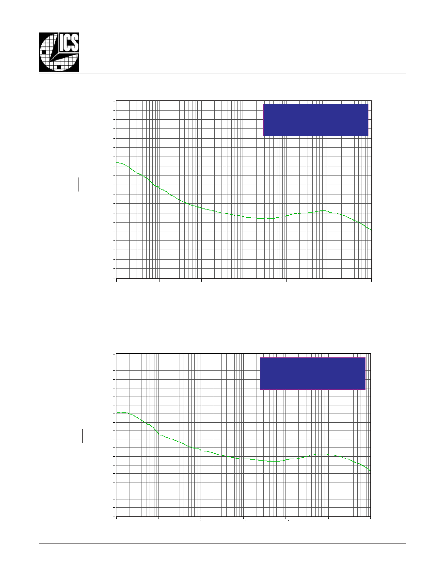
T
YPICAL
P
HASE
N
OISE
AT
155.52MH
Z
19.44MHz Input
RMS Phase Noise Jitter
12kHz to 20MHz = 3.4ps (typical)
25MHz Input
RMS Phase Noise Jitter
12kHz to 20MHz = 3.1ps (typical)
0
-10
-20
-30
-40
-50
-60
-70
-80
-90
-100
-110
-120
-130
-140
-150
-160
-170
-180
-190
10
100
1k
10k
100k
1M
10M
O
FFSET
F
REQUENCY
(H
Z
)
P
HASE
N
OISE
(
dBc
)
H
Z
O
FFSET
F
REQUENCY
(H
Z
)
P
HASE
N
OISE
(
dBc
)
H
Z
T
YPICAL
P
HASE
N
OISE
AT
156.25MH
Z
10
100
1k
10k
100k
1M
10M
0
-10
-20
-30
-40
-50
-60
-70
-80
-90
-100
-110
-120
-130
-140
-150
-160
-170
-180
-190

84427CM
www.icst.com/products/hiperclocks.html
REV. D NOVEMBER 30, 2005
6
Integrated
Circuit
Systems, Inc.
ICS84427
C
RYSTAL
-
TO
-LVDS
I
NTEGRATED
F
REQUENCY
S
YNTHESIZER
/F
ANOUT
B
UFFER
PRELIMINARY
Clock
Outputs
20%
80%
80%
20%
t
R
t
F
V
OD
t
PW
t
PERIOD
t
PW
t
PERIOD
odc =
x 100%
nQ0:nQ5
Q0:Q5
P
ARAMETER
M
EASUREMENT
I
NFORMATION
O
UTPUT
S
KEW
O
UTPUT
R
ISE
/F
ALL
T
IME
O
UTPUT
D
UTY
C
YCLE
/P
ULSE
W
IDTH
/P
ERIOD
t
sk(o)
nQx
Qx
nQy
Qy
O
FFSET
V
OLTAGE
S
ETUP
D
IFFERENTIAL
O
UTPUT
V
OLTAGE
S
ETUP
3.3V O
UTPUT
L
OAD
AC T
EST
C
IRCUIT
out
out
LVDS
DC Input
V
OS
/
V
OS
V
DD
100
out
out
LVDS
DC Input
V
OD
/
V
OD
V
DD
SCOPE
Qx
nQx
LVDS
3.3V�5%
POWER SUPPLY
+
-
Float GND

84427CM
www.icst.com/products/hiperclocks.html
REV. D NOVEMBER 30, 2005
7
Integrated
Circuit
Systems, Inc.
ICS84427
C
RYSTAL
-
TO
-LVDS
I
NTEGRATED
F
REQUENCY
S
YNTHESIZER
/F
ANOUT
B
UFFER
PRELIMINARY
A
PPLICATION
I
NFORMATION
As in any high speed analog circuitry, the power supply pins
are vulnerable to random noise. The ICS84427 provides sepa-
r a t e p o w e r s u p p l i e s t o i s o l a t e a n y h i g h s w i t c h i n g
noise from the outputs to the internal PLL. V
DD
and V
DDA
should
be individually connected to the power supply plane through
vias, and bypass capacitors should be used for each pin. To
achieve optimum jitter performance, power supply isolation is
required.
Figure 1
illustrates how a 24
resistor along with a
10
F and a .01F bypass capacitor should be connected to
each V
DDA
pin.
P
OWER
S
UPPLY
F
ILTERING
T
ECHNIQUES
F
IGURE
1. P
OWER
S
UPPLY
F
ILTERING
24
V
DDA
10
F
.01
F
3.3V
.01
F
V
DD
C
RYSTAL
I
NPUT
I
NTERFACE
The ICS84427 has been characterized with 18pF parallel
resonant crystals. The capacitor values, C1 and C2, shown
in
Figure 2
below were determined using a 25MHz, 18pF
Figure 2. C
RYSTAL
I
NPU
t I
NTERFACE
parallel resonant crystal and were chosen to minimize the
ppm error. The optimum C1 and C2 values can be slightly
adjusted for different board layouts.
C1
18p
X1
18pF Parallel Crystal
C2
22p
XTAL_IN
XTAL_OUT
84427CM
www.icst.com/products/hiperclocks.html
REV. D NOVEMBER 30, 2005
8
Integrated
Circuit
Systems, Inc.
ICS84427
C
RYSTAL
-
TO
-LVDS
I
NTEGRATED
F
REQUENCY
S
YNTHESIZER
/F
ANOUT
B
UFFER
PRELIMINARY
LVDS D
RIVER
T
ERMINATION
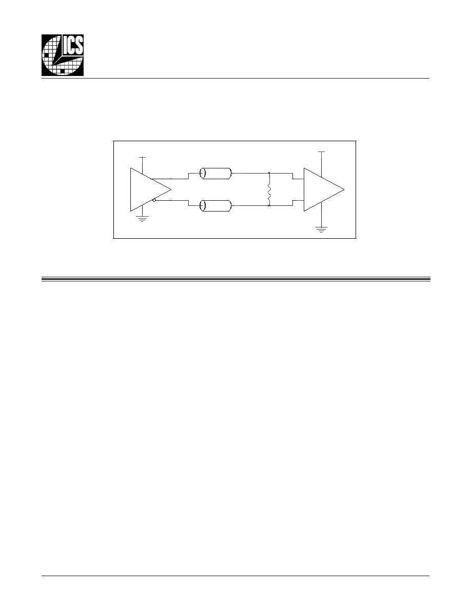
A general LVDS interface is shown in
Figure 3.
In a 100
differ-
ential transmission line environment, LVDS drivers require a
matched load termination of 100
across near the receiver in-
100 Ohm Differiential Transmission Line
R1
100
3.3V
+
-
LVDS_Driv er
3.3V
F
IGURE
3. T
YPICAL
LVDS D
RIVER
T
ERMINATION
put. For a multiple LVDS outputs buffer, if only partial outputs
are used, it is recommended to terminate the un-used outputs.
R
ECOMMENDATIONS
FOR
U
NUSED
O
UTPUT
P
INS
O
UTPUTS
:
LVDS
All unused LVDS output pairs can be either left floating or
terminated with 100
across. If they are left floating, we
recommend that there is no trace attached.

84427CM
www.icst.com/products/hiperclocks.html
REV. D NOVEMBER 30, 2005
9
Integrated
Circuit
Systems, Inc.
ICS84427
C
RYSTAL
-
TO
-LVDS
I
NTEGRATED
F
REQUENCY
S
YNTHESIZER
/F
ANOUT
B
UFFER
PRELIMINARY
F
IGURE
4A. ICS84427 S
CHEMATIC
E
XAMPLE
S
CHEMATIC
E
XAMPLE
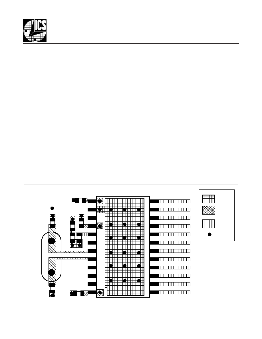
Figure 4A shows a schematic example of using an ICS84427. In
this example, the input is a 25MHz parallel resonant crystal with
load capacitor CL=18pF. The frequency fine tuning capacitors
C1 and C2 is 22pF and 18pF respectively. This example also
shows logic control input handling. The configuration is set at
F_SEL[2:0]=101, therefore, the output frequency is 156.25MHz.
It is recommended to have one decouple capacitor per power
pin. Each decoupling capacitor should be located as close as
possible to the power pin. The low pass filter R7, C11 and C16 for
clean analog supply should also be located as close to the V
DDA
pin as possible. For LVDS driver, the unused output pairs should
be terminated with a 100
resistor across.
F_SEL0
VDD
C5
0.1u
F_SEL2
VDDA
VDD
LVDS_input
+
-
RD3
SP
VDD
VDD=3.3V
VDD
F_SEL1
C11
0.1u
C2
18p
R5
1K
(U1,16)
VDD
C3
0.1u
R1
100
VDD
RU2
SP
SP = Spare, Not Installed
(U1,24)
Zo = 50
R4
1K
F_SEL0
(U1,13)
C16
10u
RU3
1K
e.g. F_SEL[2:0]=101
Zo = 50
X1
25MHz,18pF
F_SEL2
C6
0.1u
U1
ICS84427
1
2
3
4
5
6
7
8
9
10
11
12
13
14
15
16
17
18
19
20
21
22
23
24
Q0
nQ0
Q1
nQ1
Q2
nQ2
Q3
nQ3
Q4
nQ4
Q5
nQ5
VDD
VEE
PLL_SEL
VDD
VDDA
F_SEL2
XTAL_OUT
XTAL_IN
MR
F_SEL1
F_SEL0
VDD
RD1
SP
F_SEL1
RU1
1K
RD2
1K
C1
22p
R7
24
84427CM
www.icst.com/products/hiperclocks.html
REV. D NOVEMBER 30, 2005
10
Integrated
Circuit
Systems, Inc.
ICS84427
C
RYSTAL
-
TO
-LVDS
I
NTEGRATED
F
REQUENCY
S
YNTHESIZER
/F
ANOUT
B
UFFER
PRELIMINARY
The following component footprints are used in this layout
example:
All the resistors and capacitors are size 0603.
P
OWER
AND
G
ROUNDING
Place the decoupling capacitors C3, C5 and C6, as close as
possible to the power pins. If space allows, placement of the
decoupling capacitor on the component side is preferred. This
can reduce unwanted inductance between the decoupling ca-
pacitor and the power pin caused by the via.
Maximize the power and ground pad sizes and number of vias
capacitors. This can reduce the inductance between the power
and ground planes and the component power and ground pins.
The RC filter consisting of R7, C11, and C16 should be placed
as close to the V
DDA
pin as possible.
C
LOCK
T
RACES
AND
T
ERMINATION
Poor signal integrity can degrade the system performance or
cause system failure. In synchronous high-speed digital systems,
the clock signal is less tolerant to poor signal integrity than other
signals. Any ringing on the rising or falling edge or excessive ring
back can cause system failure. The shape of the trace and the
trace delay might be restricted by the available space on the board
and the component location. While routing the traces, the clock
signal traces should be routed first and should be locked prior to
routing other signal traces.
� The differential 100
output traces should have the
same length.
� Avoid sharp angles on the clock trace. Sharp angle
turns cause the characteristic impedance to change
on the transmission lines.
� Keep the clock traces on the same layer. Whenever
possible, avoid placing vias on the clock traces. Place-
ment of vias on the traces can affect the trace charac-
teristic impedance and hence degrade signal integ-
rity.
� To prevent cross talk, avoid routing other signal traces
in parallel with the clock traces. If running parallel traces
is unavoidable, allow a separation of at least three
trace widths between the differential clock trace and
the other signal trace.
� Make sure no other signal traces are routed between
the clock trace pair.
� The matching termination resistors should be located as
close to the receiver input pins as possible.
C
RYSTAL
The crystal X1 should be located as close as possible to the pins
20 (XTAL_IN) and 19 (XTAL_OUT). The trace length between
the X1 and U1 should be kept to a minimum to avoid unwanted
parasitic inductance and capacitance. Other signal traces
should not be routed near the crystal traces.
F
IGURE
4B. PCB B
OARD
L
AYOUT
FOR
ICS84427
VDDA
X1
C1
C5
U1
Signals
C6
ICS84427
VDD
C2
Pin1
C3
VIA
C16
C11
50 Ohm Traces
R7
GND

84427CM
www.icst.com/products/hiperclocks.html
REV. D NOVEMBER 30, 2005
11
Integrated
Circuit
Systems, Inc.
ICS84427
C
RYSTAL
-
TO
-LVDS
I
NTEGRATED
F
REQUENCY
S
YNTHESIZER
/F
ANOUT
B
UFFER
PRELIMINARY
R
ELIABILITY
I
NFORMATION
T
RANSISTOR
C
OUNT
The transistor count for ICS84427 is: 2804
T
ABLE
7.
JA
VS
. A
IR
F
LOW
T
ABLE
FOR
24 L
EAD
SOIC
JA
by Velocity (Linear Feet per Minute)
0
200
500
Multi-Layer PCB, JEDEC Standard Test Boards
50�C/W
43�C/W
38�C/W
NOTE: Most modern PCB designs use multi-layered boards. The data in the second row pertains to most designs.

84427CM
www.icst.com/products/hiperclocks.html
REV. D NOVEMBER 30, 2005
12
Integrated
Circuit
Systems, Inc.
ICS84427
C
RYSTAL
-
TO
-LVDS
I
NTEGRATED
F
REQUENCY
S
YNTHESIZER
/F
ANOUT
B
UFFER
PRELIMINARY
P
ACKAGE
O
UTLINE
- M S
UFFIX
FOR
24 L
EAD
SOIC
T
ABLE
8. P
ACKAGE
D
IMENSIONS
Reference Document: JEDEC Publication 95, MS-013, MO-119
L
O
B
M
Y
S
s
r
e
t
e
m
i
l
l
i
M
m
u
m
i
n
i
M
m
u
m
i
x
a
M
N
4
2
A
-
-
5
6
.
2
1
A
0
1
.
0
-
-
2
A
5
0
.
2
5
5
.
2
B
3
3
.
0
1
5
.
0
C
8
1
.
0
2
3
.
0
D
0
2
.
5
1
5
8
.
5
1
E
0
4
.
7
0
6
.
7
e
C
I
S
A
B
7
2
.
1
H
0
0
.
0
1
5
6
.
0
1
h
5
2
.
0
5
7
.
0
L
0
4
.
0
7
2
.
1
�
0
�
8

84427CM
www.icst.com/products/hiperclocks.html
REV. D NOVEMBER 30, 2005
13
Integrated
Circuit
Systems, Inc.
ICS84427
C
RYSTAL
-
TO
-LVDS
I
NTEGRATED
F
REQUENCY
S
YNTHESIZER
/F
ANOUT
B
UFFER
PRELIMINARY
T
ABLE
9. O
RDERING
I
NFORMATION
While the information presented herein has been checked for both accuracy and reliability, Integrated Circuit Systems, Incorporated (ICS) assumes no responsibility for either its use
or for infringement of any patents or other rights of third parties, which would result from its use. No other circuits, patents, or licenses are implied. This product is intended for use
in normal commercial applications. Any other applications such as those requiring extended temperature range, high reliability, or other extraordinary environmental requirements are
not recommended without additional processing by ICS. ICS reserves the right to change any circuitry or specifications without notice. ICS does not authorize or warrant any ICS
product for use in life support devices or critical medical instruments.
The aforementioned trademark, HiPerClockS is a trademark of Integrated Circuit Systems, Inc. or its subsidiaries in the United States and/or other countries.
r
e
b
m
u
N
r
e
d
r
O
/
t
r
a
P
g
n
i
k
r
a
M
e
g
a
k
c
a
P
g
n
i
g
a
k
c
a
P
g
n
i
p
p
i
h
S
e
r
u
t
a
r
e
p
m
e
T
M
C
7
2
4
4
8
S
C
I
M
C
7
2
4
4
8
S
C
I
C
I
O
S
d
a
e
L
4
2
e
b
u
t
C
�
0
7
o
t
C
�
0
T
M
C
7
2
4
4
8
S
C
I
M
C
7
2
4
4
8
S
C
I
C
I
O
S
d
a
e
L
4
2
l
e
e
r
&
e
p
a
t
0
0
0
1
C
�
0
7
o
t
C
�
0
F
L
M
C
7
2
4
4
8
S
C
I
F
L
M
C
7
2
4
4
8
S
C
I
C
I
O
S
"
e
e
r
F
-
d
a
e
L
"
d
a
e
L
4
2
e
b
u
t
C
�
0
7
o
t
C
�
0
T
F
L
M
C
7
2
4
4
8
S
C
I
F
L
M
C
7
2
4
4
8
S
C
I
C
I
O
S
"
e
e
r
F
-
d
a
e
L
"
d
a
e
L
4
2
l
e
e
r
&
e
p
a
t
0
0
0
1
C
�
0
7
o
t
C
�
0
.
t
n
i
a
l
p
m
o
c
S
H
o
R
e
r
a
d
n
a
n
o
i
t
a
r
u
g
i
f
n
o
c
e
e
r
F
-
b
P
e
h
t
e
r
a
r
e
b
m
u
n
t
r
a
p
e
h
t
o
t
x
i
f
f
u
s
"
F
L
"
n
a
h
t
i
w
d
e
r
e
d
r
o
e
r
a
t
a
h
t
s
t
r
a
P
:
E
T
O
N