Document Outline
- General Description
- Features
- Block Diagram
- Pin Assignment
- Pin Descriptions
- Pin Characteristics
- Control Input Function Table
- Clock Input Function Table
- Absolute Maximum Ratings
- Power Supply DC Characteristics
- LVCMOS DC Characteristics
- Differential DC Characteristics
- LVDS DC Characteristics
- AC Characteristics
- Additive Phase Jitter
- Parameter Measurement Information
- Parameter Measurement Information, continued
- Application Information
- Wiring the Differential Input to Accept Single Ended Levels
- Recommendations for Unused Input & Output Pins
- Differential Clock Input Interface
- LVDS Driver Termination
- Schematic Example
- Reliability Information
- Transistor Count
- Package Outline
- Package Dimensions
- Ordering Information
- Revision History Sheet

8516FY
www.icst.com/products/hiperclocks.html
REV. B FEBRUARY 21, 2006
1
Integrated
Circuit
Systems, Inc.
ICS8516
L
OW
S
KEW
, 1-
TO
-16
D
IFFERENTIAL
-
TO
-LVDS C
LOCK
D
ISTRIBUTION
C
HIP
G
ENERAL
D
ESCRIPTION
The ICS8516 is a low skew, high performance
1-to-16 Differential-to-LVDS Clock Distribution
Chip and a member of the HiPerClock S TM
family of High Performance Clock Solutions from
ICS. The ICS8516 CLK, nCLK pair can accept
any differential input levels and translates them to 3.3V LVDS
output levels. Utilizing Low Voltage Differential Signaling
(LVDS), the ICS8516 provides a low power, low noise, point-
to-point solution for distributing clock signals over controlled
impedances of 100
.
Dual output enable inputs allow the ICS8516 to be used in a
1-to-16 or 1-to-8 input/output mode.
Guaranteed output and part-to-part skew specifications make
the ICS8516 ideal for those applications demanding well
defined performance and repeatability.
B
LOCK
D
IAGRAM
P
IN
A
SSIGNMENT
F
EATURES
∑ Sixteen differential LVDS outputs
∑ CLK, nCLK pair can accept the following differential
input levels: LVPECL, LVDS, LVHSTL, HCSL, SSTL
∑ Maximum output frequency: 700MHz
∑ Translates any differential input signal (LVPECL, LVHSTL,
SSTL, DCM) to LVDS levels without external bias networks
∑ Translates any single-ended input signal to LVDS
with resistor bias on nCLK input
∑ Multiple output enable inputs for disabling unused
outputs in reduced fanout applications
∑ LVDS compatible
∑ Output skew: 90ps (maximum)
∑ Part-to-part skew: 500ps (maximum)
∑ Propagation delay: 2.4ns (maximum)
∑ Additive phase jitter, RMS: 148fs (typical)
∑ 3.3V operating supply
∑ 0∞C to 70∞C ambient operating temperature
∑ Available in both standard and lead-free RoHS compliant
packages
HiPerClockSTM
ICS
48-Lead LQFP
7mm x 7mm x 1.4mm body package
Y Package
Top View
OE1
OE2
CLK
nCLK
Q0
nQ0
Q1
nQ1
Q2
nQ2
Q3
nQ3
Q4
nQ4
Q5
nQ5
Q6
nQ6
Q7
nQ7
Q15
nQ15
Q14
nQ14
Q13
nQ13
Q12
nQ12
Q11
nQ11
Q10
nQ10
Q9
nQ9
Q8
nQ8
48 47 46 45 44 43 42 41 40 39 38 37
13 14 15 16 17 18 19 20 21 22 23 24
1
2
3
4
5
6
7
8
9
10
11
12
36
35
34
33
32
31
30
29
28
27
26
25
V
DD
nQ5
Q5
nQ4
Q4
V
DD
GND
nQ3
Q3
nQ2
Q2
V
DD
V
DD
nQ10
Q10
nQ11
Q11
V
DD
GND
nQ12
Q12
nQ13
Q13
V
DD
nQ14
Q14
nQ15
Q15
GND
CLK
nCLK
GND
Q0
nQ0
Q1
nQ1
ICS8516
Q9
nQ9
Q8
nQ8
GND
OE2
OE1
GND
nQ7
Q7
nQ6
Q6

8516FY
www.icst.com/products/hiperclocks.html
REV. B FEBRUARY 21, 2006
2
Integrated
Circuit
Systems, Inc.
ICS8516
L
OW
S
KEW
, 1-
TO
-16
D
IFFERENTIAL
-
TO
-LVDS C
LOCK
D
ISTRIBUTION
C
HIP
T
ABLE
1. P
IN
D
ESCRIPTIONS
r
e
b
m
u
N
e
m
a
N
e
p
y
T
n
o
i
t
p
i
r
c
s
e
D
,
2
1
,
6
,
1
6
3
,
1
3
,
5
2
V
D
D
r
e
w
o
P
.
s
n
i
p
y
l
p
p
u
s
e
v
i
t
i
s
o
P
3
,
2
5
Q
,
5
Q
n
t
u
p
t
u
O
.
s
l
e
v
e
l
e
c
a
f
r
e
t
n
i
S
D
V
L
.
r
i
a
p
t
u
p
t
u
o
l
a
i
t
n
e
r
e
f
f
i
D
5
,
4
4
Q
,
4
Q
n
t
u
p
t
u
O
.
s
l
e
v
e
l
e
c
a
f
r
e
t
n
i
S
D
V
L
.
r
i
a
p
t
u
p
t
u
o
l
a
i
t
n
e
r
e
f
f
i
D
,
0
2
,
7
1
,
7
4
4
,
1
4
,
0
3
D
N
G
r
e
w
o
P
.
d
n
u
o
r
g
y
l
p
p
u
s
r
e
w
o
P
9
,
8
3
Q
,
3
Q
n
t
u
p
t
u
O
.
s
l
e
v
e
l
e
c
a
f
r
e
t
n
i
S
D
V
L
.
r
i
a
p
t
u
p
t
u
o
l
a
i
t
n
e
r
e
f
f
i
D
1
1
,
0
1
2
Q
,
2
Q
n
t
u
p
t
u
O
.
s
l
e
v
e
l
e
c
a
f
r
e
t
n
i
S
D
V
L
.
r
i
a
p
t
u
p
t
u
o
l
a
i
t
n
e
r
e
f
f
i
D
4
1
,
3
1
1
Q
,
1
Q
n
t
u
p
t
u
O
.
s
l
e
v
e
l
e
c
a
f
r
e
t
n
i
S
D
V
L
.
r
i
a
p
t
u
p
t
u
o
l
a
i
t
n
e
r
e
f
f
i
D
6
1
,
5
1
0
Q
,
0
Q
n
t
u
p
t
u
O
.
s
l
e
v
e
l
e
c
a
f
r
e
t
n
i
S
D
V
L
.
r
i
a
p
t
u
p
t
u
o
l
a
i
t
n
e
r
e
f
f
i
D
8
1
K
L
C
n
t
u
p
n
I
p
u
ll
u
P
.
t
u
p
n
i
k
c
o
l
c
l
a
i
t
n
e
r
e
f
f
i
d
g
n
i
t
r
e
v
n
I
9
1
K
L
C
t
u
p
n
I
n
w
o
d
ll
u
P
.
t
u
p
n
i
k
c
o
l
c
l
a
i
t
n
e
r
e
f
f
i
d
g
n
i
t
r
e
v
n
i
-
n
o
N
2
2
,
1
2
5
1
Q
n
,
5
1
Q
t
u
p
t
u
O
.
s
l
e
v
e
l
e
c
a
f
r
e
t
n
i
S
D
V
L
.
r
i
a
p
t
u
p
t
u
o
l
a
i
t
n
e
r
e
f
f
i
D
4
2
,
3
2
4
1
Q
n
,
4
1
Q
t
u
p
t
u
O
.
s
l
e
v
e
l
e
c
a
f
r
e
t
n
i
S
D
V
L
.
r
i
a
p
t
u
p
t
u
o
l
a
i
t
n
e
r
e
f
f
i
D
7
2
,
6
2
3
1
Q
n
,
3
1
Q
t
u
p
t
u
O
.
s
l
e
v
e
l
e
c
a
f
r
e
t
n
i
S
D
V
L
.
r
i
a
p
t
u
p
t
u
o
l
a
i
t
n
e
r
e
f
f
i
D
9
2
,
8
2
2
1
Q
n
,
2
1
Q
t
u
p
t
u
O
.
s
l
e
v
e
l
e
c
a
f
r
e
t
n
i
S
D
V
L
.
r
i
a
p
t
u
p
t
u
o
l
a
i
t
n
e
r
e
f
f
i
D
3
3
,
2
3
1
1
Q
n
,
1
1
Q
t
u
p
t
u
O
.
s
l
e
v
e
l
e
c
a
f
r
e
t
n
i
S
D
V
L
.
r
i
a
p
t
u
p
t
u
o
l
a
i
t
n
e
r
e
f
f
i
D
5
3
,
4
3
0
1
Q
n
,
0
1
Q
t
u
p
t
u
O
.
s
l
e
v
e
l
e
c
a
f
r
e
t
n
i
S
D
V
L
.
r
i
a
p
t
u
p
t
u
o
l
a
i
t
n
e
r
e
f
f
i
D
8
3
,
7
3
9
Q
n
,
9
Q
t
u
p
t
u
O
.
s
l
e
v
e
l
e
c
a
f
r
e
t
n
i
S
D
V
L
.
r
i
a
p
t
u
p
t
u
o
l
a
i
t
n
e
r
e
f
f
i
D
0
4
,
9
3
8
Q
n
,
8
Q
t
u
p
t
u
O
.
s
l
e
v
e
l
e
c
a
f
r
e
t
n
i
S
D
V
L
.
r
i
a
p
t
u
p
t
u
o
l
a
i
t
n
e
r
e
f
f
i
D
3
4
,
2
4
1
E
O
,
2
E
O
t
u
p
n
I
p
u
ll
u
P
;
5
1
Q
n
,
5
1
Q
u
r
h
t
8
Q
n
,
8
Q
s
t
u
p
t
u
o
s
l
o
r
t
n
o
c
2
E
O
.
e
l
b
a
n
e
t
u
p
t
u
O
.
7
Q
n
,
7
Q
u
r
h
t
0
Q
n
,
0
Q
s
t
u
p
t
u
o
s
l
o
r
t
n
o
c
1
E
O
.
s
l
e
v
e
l
e
c
a
f
r
e
t
n
i
L
T
T
V
L
/
S
O
M
C
V
L
6
4
,
5
4
7
Q
,
7
Q
n
t
u
p
t
u
O
.
s
l
e
v
e
l
e
c
a
f
r
e
t
n
i
S
D
V
L
.
r
i
a
p
t
u
p
t
u
o
l
a
i
t
n
e
r
e
f
f
i
D
8
4
,
7
4
6
Q
,
6
Q
n
t
u
p
t
u
O
.
s
l
e
v
e
l
e
c
a
f
r
e
t
n
i
S
D
V
L
.
r
i
a
p
t
u
p
t
u
o
l
a
i
t
n
e
r
e
f
f
i
D
:
E
T
O
N
p
u
ll
u
P
d
n
a
n
w
o
d
ll
u
P
.
s
e
u
l
a
v
l
a
c
i
p
y
t
r
o
f
,
s
c
i
t
s
i
r
e
t
c
a
r
a
h
C
n
i
P
,
2
e
l
b
a
T
e
e
S
.
s
r
o
t
s
i
s
e
r
t
u
p
n
i
l
a
n
r
e
t
n
i
o
t
r
e
f
e
r

8516FY
www.icst.com/products/hiperclocks.html
REV. B FEBRUARY 21, 2006
3
Integrated
Circuit
Systems, Inc.
ICS8516
L
OW
S
KEW
, 1-
TO
-16
D
IFFERENTIAL
-
TO
-LVDS C
LOCK
D
ISTRIBUTION
C
HIP
T
ABLE
2. P
IN
C
HARACTERISTICS
T
ABLE
3A. C
ONTROL
I
NPUT
F
UNCTION
T
ABLE
T
ABLE
3B. C
LOCK
I
NPUT
F
UNCTION
T
ABLE
s
t
u
p
n
I
s
t
u
p
t
u
O
1
E
O
2
E
O
7
Q
:
0
Q
7
Q
n
:
0
Q
n
5
1
Q
:
8
Q
5
1
Q
n
:
8
Q
n
0
0
Z
i
H
Z
i
H
Z
i
H
Z
i
H
1
0
E
V
I
T
C
A
E
V
I
T
C
A
Z
i
H
Z
i
H
0
1
Z
i
H
Z
i
H
E
V
I
T
C
A
E
V
I
T
C
A
1
1
E
V
I
T
C
A
E
V
I
T
C
A
E
V
I
T
C
A
E
V
I
T
C
A
.
B
3
e
l
b
a
T
n
i
d
e
b
i
r
c
s
e
d
s
a
s
t
u
p
n
i
K
L
C
n
d
n
a
K
L
C
e
h
t
f
o
n
o
i
t
c
n
u
f
a
e
r
a
s
t
u
p
t
u
o
e
h
t
f
o
e
t
a
t
s
e
h
t
,
e
d
o
m
e
v
i
t
c
a
e
h
t
n
I
s
t
u
p
n
I
s
t
u
p
t
u
O
e
d
o
M
t
u
p
t
u
O
o
t
t
u
p
n
I
y
t
i
r
a
l
o
P
K
L
C
K
L
C
n
5
1
Q
:
0
Q
5
1
Q
n
:
0
Q
n
0
1
W
O
L
H
G
I
H
l
a
i
t
n
e
r
e
f
f
i
D
o
t
l
a
i
t
n
e
r
e
f
f
i
D
g
n
i
t
r
e
v
n
I
n
o
N
1
0
H
G
I
H
W
O
L
l
a
i
t
n
e
r
e
f
f
i
D
o
t
l
a
i
t
n
e
r
e
f
f
i
D
g
n
i
t
r
e
v
n
I
n
o
N
0
1
E
T
O
N
;
d
e
s
a
i
B
W
O
L
H
G
I
H
l
a
i
t
n
e
r
e
f
f
i
D
o
t
d
e
d
n
E
e
l
g
n
i
S
g
n
i
t
r
e
v
n
I
n
o
N
1
1
E
T
O
N
;
d
e
s
a
i
B
H
G
I
H
W
O
L
l
a
i
t
n
e
r
e
f
f
i
D
o
t
d
e
d
n
E
e
l
g
n
i
S
g
n
i
t
r
e
v
n
I
n
o
N
1
E
T
O
N
;
d
e
s
a
i
B
0
H
G
I
H
W
O
L
l
a
i
t
n
e
r
e
f
f
i
D
o
t
d
e
d
n
E
e
l
g
n
i
S
g
n
i
t
r
e
v
n
I
1
E
T
O
N
;
d
e
s
a
i
B
1
W
O
L
H
G
I
H
l
a
i
t
n
e
r
e
f
f
i
D
o
t
d
e
d
n
E
e
l
g
n
i
S
g
n
i
t
r
e
v
n
I
.
"
s
l
e
v
e
L
d
e
d
n
E
e
l
g
n
i
S
t
p
e
c
c
A
o
t
t
u
p
n
I
l
a
i
t
n
e
r
e
f
f
i
D
e
h
t
g
n
i
r
i
W
"
,
n
o
i
t
c
e
s
n
o
i
t
a
m
r
o
f
n
I
n
o
i
t
a
c
il
p
p
A
e
h
t
o
t
r
e
f
e
r
e
s
a
e
l
P
:
1
E
T
O
N
l
o
b
m
y
S
r
e
t
e
m
a
r
a
P
s
n
o
i
t
i
d
n
o
C
t
s
e
T
m
u
m
i
n
i
M
l
a
c
i
p
y
T
m
u
m
i
x
a
M
s
t
i
n
U
C
N
I
e
c
n
a
t
i
c
a
p
a
C
t
u
p
n
I
4
F
p
R
P
U
L
L
U
P
r
o
t
s
i
s
e
R
p
u
ll
u
P
t
u
p
n
I
1
5
k
R
N
W
O
D
L
L
U
P
r
o
t
s
i
s
e
R
n
w
o
d
ll
u
P
t
u
p
n
I
1
5
k
C
D
P
e
c
n
a
t
i
c
a
p
a
C
n
o
i
t
a
p
i
s
s
i
D
r
e
w
o
P
)
t
u
p
t
u
o
r
e
p
(
4
F
p
8516FY
www.icst.com/products/hiperclocks.html
REV. B FEBRUARY 21, 2006
4
Integrated
Circuit
Systems, Inc.
ICS8516
L
OW
S
KEW
, 1-
TO
-16
D
IFFERENTIAL
-
TO
-LVDS C
LOCK
D
ISTRIBUTION
C
HIP
T
ABLE
4A. P
OWER
S
UPPLY
DC C
HARACTERISTICS
,
V
DD
= 3.3V±5%, T
A
= 0∞C
TO
70∞C
T
ABLE
4C. D
IFFERENTIAL
DC C
HARACTERISTICS
,
V
DD
= 3.3V±5%, T
A
= 0∞C
TO
70∞C
T
ABLE
4B. LVCMOS/LVTTL DC C
HARACTERISTICS
,
V
DD
= 3.3V±5%, T
A
= 0∞C
TO
70∞C
l
o
b
m
y
S
r
e
t
e
m
a
r
a
P
s
n
o
i
t
i
d
n
o
C
t
s
e
T
m
u
m
i
n
i
M
l
a
c
i
p
y
T
m
u
m
i
x
a
M
s
t
i
n
U
V
D
D
e
g
a
t
l
o
V
y
l
p
p
u
S
e
v
i
t
i
s
o
P
5
3
1
.
3
3
.
3
5
6
4
.
3
V
I
D
D
t
n
e
r
r
u
C
y
l
p
p
u
S
r
e
w
o
P
c
i
t
a
t
S
R
L
0
0
1
=
5
3
1
5
6
1
A
m
d
a
o
L
o
N
0
6
5
7
A
m
l
o
b
m
y
S
r
e
t
e
m
a
r
a
P
s
n
o
i
t
i
d
n
o
C
t
s
e
T
m
u
m
i
n
i
M
l
a
c
i
p
y
T
m
u
m
i
x
a
M
s
t
i
n
U
I
H
I
t
n
e
r
r
u
C
h
g
i
H
t
u
p
n
I
K
L
C
V
N
I
V
=
D
D
V
5
6
4
.
3
=
0
5
1
A
µ
K
L
C
n
V
N
I
V
=
D
D
V
5
6
4
.
3
=
5
A
µ
I
L
I
t
n
e
r
r
u
C
w
o
L
t
u
p
n
I
K
L
C
V
D
D
V
,
V
5
6
4
.
3
=
N
I
V
0
=
5
-
A
µ
K
L
C
n
V
D
D
V
,
V
5
6
4
.
3
=
N
I
V
0
=
0
5
1
-
A
µ
V
P
P
e
g
a
t
l
o
V
k
a
e
P
-
o
t
-
k
a
e
P
5
1
.
0
3
.
1
V
V
R
M
C
;
e
g
a
t
l
o
V
t
u
p
n
I
e
d
o
M
n
o
m
m
o
C
2
,
1
E
T
O
N
5
.
0
+
D
N
G
V
D
D
5
8
.
0
-
V
V
s
i
K
L
C
n
,
K
L
C
r
o
f
e
g
a
t
l
o
v
t
u
p
n
i
m
u
m
i
x
a
m
e
h
t
,
s
n
o
i
t
a
c
il
p
p
a
d
e
d
n
e
e
l
g
n
i
s
r
o
F
:
1
E
T
O
N
D
D
.
V
3
.
0
+
t
s
a
d
e
n
i
f
e
d
s
i
e
g
a
t
l
o
v
e
d
o
m
n
o
m
m
o
C
:
2
E
T
O
N
V
H
I
.
l
o
b
m
y
S
r
e
t
e
m
a
r
a
P
s
n
o
i
t
i
d
n
o
C
t
s
e
T
m
u
m
i
n
i
M
l
a
c
i
p
y
T
m
u
m
i
x
a
M
s
t
i
n
U
V
H
I
e
g
a
t
l
o
V
h
g
i
H
t
u
p
n
I
2
E
O
,
1
E
O
2
V
D
D
3
.
0
+
V
V
L
I
e
g
a
t
l
o
V
w
o
L
t
u
p
n
I
2
E
O
,
1
E
O
3
.
0
-
8
.
0
V
I
H
I
t
n
e
r
r
u
C
h
g
i
H
t
u
p
n
I
2
E
O
,
1
E
O
V
D
D
V
=
N
I
V
5
6
4
.
3
=
5
A
µ
I
L
I
t
n
e
r
r
u
C
w
o
L
t
u
p
n
I
2
E
O
,
1
E
O
V
D
D
V
,
V
5
6
4
.
3
=
N
I
V
0
=
0
5
1
-
A
µ
A
BSOLUTE
M
AXIMUM
R
ATINGS
Supply Voltage, V
DD
4.6V
Inputs, V
I
-0.5V to V
DD
+ 0.5 V
Outputs, V
O
-0.5V to V
DD
+ 0.5V
Package Thermal Impedance,
JA
47.9∞C/W (0 lfpm)
Storage Temperature, T
STG
-65∞C to 150∞C
NOTE: Stresses beyond those listed under Absolute
Maximum Ratings may cause permanent damage to the
device. These ratings are stress specifications only. Functional
operation of product at these conditions or any conditions be-
yond those listed in the
DC Characteristics
or
AC Character-
istics
is not implied. Exposure to absolute maximum rating
conditions for extended periods may affect product reliability.
8516FY
www.icst.com/products/hiperclocks.html
REV. B FEBRUARY 21, 2006
5
Integrated
Circuit
Systems, Inc.
ICS8516
L
OW
S
KEW
, 1-
TO
-16
D
IFFERENTIAL
-
TO
-LVDS C
LOCK
D
ISTRIBUTION
C
HIP
T
ABLE
5. AC C
HARACTERISTICS
,
V
DD
= 3.3V±5%, T
A
= 0∞C
TO
70∞C
T
ABLE
4D. LVDS DC C
HARACTERISTICS
,
V
DD
= 3.3V±5%, T
A
= 0∞C
TO
70∞C
l
o
b
m
y
S
r
e
t
e
m
a
r
a
P
s
n
o
i
t
i
d
n
o
C
t
s
e
T
m
u
m
i
n
i
M
l
a
c
i
p
y
T
m
u
m
i
x
a
M
s
t
i
n
U
V
D
O
e
g
a
t
l
o
V
t
u
p
t
u
O
l
a
i
t
n
e
r
e
f
f
i
D
0
5
2
0
0
4
0
0
6
V
m
V
D
O
V
D
O
e
g
n
a
h
C
e
d
u
t
i
n
g
a
M
0
5
V
m
V
S
O
e
g
a
t
l
o
V
t
e
s
f
f
O
5
2
1
.
1
4
.
1
6
.
1
V
V
S
O
V
S
O
e
g
n
a
h
C
e
d
u
t
i
n
g
a
M
0
5
V
m
I
Z
O
t
n
e
r
r
u
C
e
g
a
k
a
e
L
e
c
n
a
d
e
p
m
I
h
g
i
H
0
1
-
0
1
+
A
µ
I
F
F
O
e
g
a
k
a
e
L
f
f
O
r
e
w
o
P
1
-
1
+
A
µ
I
D
S
O
t
n
e
r
r
u
C
t
i
u
c
r
i
C
t
r
o
h
S
t
u
p
t
u
O
l
a
i
t
n
e
r
e
f
f
i
D
5
.
5
-
A
m
I
S
O
I
/
B
S
O
t
n
e
r
r
u
C
t
i
u
c
r
i
C
t
r
o
h
S
t
u
p
t
u
O
2
1
-
A
m
l
o
b
m
y
S
r
e
t
e
m
a
r
a
P
s
n
o
i
t
i
d
n
o
C
t
s
e
T
m
u
m
i
n
i
M
l
a
c
i
p
y
T
m
u
m
i
x
a
M
s
t
i
n
U
f
X
A
M
y
c
n
e
u
q
e
r
F
t
u
p
t
u
O
0
0
7
z
H
M
t
D
P
1
E
T
O
N
;
y
a
l
e
D
n
o
i
t
a
g
a
p
o
r
P
6
.
1
0
.
2
4
.
2
s
n
t
)
o
(
k
s
4
,
2
E
T
O
N
;
w
e
k
S
t
u
p
t
u
O
0
9
s
p
t
)
p
p
(
k
s
4
,
3
E
T
O
N
;
w
e
k
S
t
r
a
P
-
o
t
-
t
r
a
P
0
0
5
s
p
t
t
ij
;
S
M
R
,
r
e
t
t
i
J
e
s
a
h
P
e
v
i
t
i
d
d
A
r
e
f
f
u
B
n
o
i
t
c
e
S
r
e
t
t
i
J
e
s
a
h
P
e
v
i
t
i
d
d
A
o
t
r
e
f
e
r
:
e
g
n
a
R
n
o
i
t
a
r
g
e
t
n
I
z
H
M
0
2
-
z
H
k
2
1
8
4
1
s
f
t
R
t
/
F
e
m
i
T
ll
a
F
/
e
s
i
R
t
u
p
t
u
O
%
0
8
o
t
%
0
2
0
0
1
0
5
5
s
p
c
d
o
e
l
c
y
C
y
t
u
D
t
u
p
t
u
O
5
4
0
5
5
5
%
t
L
Z
P
t
,
H
Z
P
5
E
T
O
N
;
e
m
i
T
e
l
b
a
n
E
t
u
p
t
u
O
5
s
n
t
Z
L
P
t
,
Z
H
P
5
E
T
O
N
;
e
m
i
T
e
l
b
a
s
i
D
t
u
p
t
u
O
5
s
n
.
t
n
i
o
p
g
n
i
s
s
o
r
c
t
u
p
t
u
o
l
a
i
t
n
e
r
e
f
f
i
d
e
h
t
o
t
t
n
i
o
p
g
n
i
s
s
o
r
c
t
u
p
n
i
l
a
i
t
n
e
r
e
f
f
i
d
e
h
t
m
o
r
f
d
e
r
u
s
a
e
M
:
1
E
T
O
N
.
s
n
o
i
t
i
d
n
o
c
d
a
o
l
l
a
u
q
e
h
t
i
w
d
n
a
s
e
g
a
t
l
o
v
y
l
p
p
u
s
e
m
a
s
e
h
t
t
a
s
t
u
p
t
u
o
n
e
e
w
t
e
b
w
e
k
s
s
a
d
e
n
i
f
e
D
:
2
E
T
O
N
.
s
t
n
i
o
p
s
s
o
r
c
l
a
i
t
n
e
r
e
f
f
i
d
t
u
p
t
u
o
e
h
t
t
a
d
e
r
u
s
a
e
M
s
e
g
a
t
l
o
v
y
l
p
p
u
s
e
m
a
s
e
h
t
t
a
g
n
i
t
a
r
e
p
o
s
e
c
i
v
e
d
t
n
e
r
e
f
f
i
d
n
o
s
t
u
p
t
u
o
n
e
e
w
t
e
b
w
e
k
s
s
a
d
e
n
i
f
e
D
:
3
E
T
O
N
d
e
r
u
s
a
e
m
e
r
a
s
t
u
p
t
u
o
e
h
t
,
e
c
i
v
e
d
h
c
a
e
n
o
s
t
u
p
n
i
f
o
e
p
y
t
e
m
a
s
e
h
t
g
n
i
s
U
.
s
n
o
i
t
i
d
n
o
c
d
a
o
l
l
a
u
q
e
h
t
i
w
d
n
a
.
s
t
n
i
o
p
s
s
o
r
c
l
a
i
t
n
e
r
e
f
f
i
d
e
h
t
t
a
.
5
6
d
r
a
d
n
a
t
S
C
E
D
E
J
h
t
i
w
e
c
n
a
d
r
o
c
c
a
n
i
d
e
n
i
f
e
d
s
i
r
e
t
e
m
a
r
a
p
s
i
h
T
:
4
E
T
O
N
.
n
o
i
t
c
u
d
o
r
p
n
i
d
e
t
s
e
t
t
o
N
.
n
o
i
t
a
z
i
r
e
t
c
a
r
a
h
c
y
b
d
e
e
t
n
a
r
a
u
g
e
r
a
s
r
e
t
e
m
a
r
a
p
e
s
e
h
T
:
5
E
T
O
N

8516FY
www.icst.com/products/hiperclocks.html
REV. B FEBRUARY 21, 2006
6
Integrated
Circuit
Systems, Inc.
ICS8516
L
OW
S
KEW
, 1-
TO
-16
D
IFFERENTIAL
-
TO
-LVDS C
LOCK
D
ISTRIBUTION
C
HIP
A
DDITIVE
P
HASE
J
ITTER
Additive Phase Jitter
@ 155.52MHz
(12kHz to 20MHz)
= 148fs typical
-50
-60
-70
-80
-90
-100
-100
-120
-130
-140
-150
-160
1k
10k
100k
1M
10M
100M
The spectral purity in a band at a specific offset from the
fundamental compared to the power of the fundamental is
called the
dBc Phase Noise.
This value is normally expressed
using a Phase noise plot and is most often the specified plot
in many applications. Phase noise is defined as the ratio of
the noise power present in a 1Hz band at a specified offset
from the fundamental frequency to the power value of the
fundamental. This ratio is expressed in decibels (dBm) or a
As with most timing specifications, phase noise measure-
ments have issues. The primary issue relates to the limita-
tions of the equipment. Often the noise floor of the equipment
is higher than the noise floor of the device. This is illustrated
ratio of the power in the 1Hz band to the power in the funda-
mental. When the required offset is specified, the phase noise
is called a
dBc
value, which simply means dBm at a specified
offset from the fundamental. By investigating jitter in the fre-
quency domain, we get a better understanding of its effects
on the desired application over the entire time record of the
signal. It is mathematically possible to calculate an expected
bit error rate given a phase noise plot.
above. The device meets the noise floor of what is shown, but
can actually be lower. The phase noise is dependant on the
input source and measurement equipment.
O
FFSET
F
ROM
C
ARRIER
F
REQUENCY
(H
Z
)
SSB P
HASE
N
OISE
dB
c/H
Z

8516FY
www.icst.com/products/hiperclocks.html
REV. B FEBRUARY 21, 2006
7
Integrated
Circuit
Systems, Inc.
ICS8516
L
OW
S
KEW
, 1-
TO
-16
D
IFFERENTIAL
-
TO
-LVDS C
LOCK
D
ISTRIBUTION
C
HIP
P
ARAMETER
M
EASUREMENT
I
NFORMATION
P
ART
-
TO
-P
ART
S
KEW
P
ROPAGATION
D
ELAY
O
UTPUT
R
ISE
/F
ALL
T
IME
Clock
Outputs
20%
80%
80%
20%
t
R
t
F
V
OD
t
sk(o)
nQx
nQ
nQy
Qy
D
IFFERENTIAL
I
NPUT
L
EVEL
O
UTPUT
S
KEW
3.3V O
UTPUT
L
OAD
AC T
EST
C
IRCUIT
SCOPE
Qx
nQx
LVDS
Power Supply
+
-
Float GND
V
CMR
Cross Points
V
PP
GND
CLK
nCLK
V
DD
t
sk(pp)
nQx
Qx
nQy
Qy
PART 1
PART 2
nCLK
CLK
nQ0:nQ15
Q0:Q15
t
PD
3.3V ± 5%
8516FY
www.icst.com/products/hiperclocks.html
REV. B FEBRUARY 21, 2006
8
Integrated
Circuit
Systems, Inc.
ICS8516
L
OW
S
KEW
, 1-
TO
-16
D
IFFERENTIAL
-
TO
-LVDS C
LOCK
D
ISTRIBUTION
C
HIP
O
UTPUT
D
UTY
C
YCLE
/P
ULSE
W
IDTH
/P
ERIOD
O
FFSET
V
OLTAGE
S
ETUP
t
PW
t
PERIOD
t
PW
t
PERIOD
odc =
x 100%
nQ0:nQ15
Q0:Q15
P
OWER
O
FF
L
EAKAGE
S
ETUP
D
IFFERENTIAL
O
UTPUT
S
HORT
CIRCUIT
C
URRENT
S
ETUP
O
UTPUT
S
HORT
C
IRCUIT
C
URRENT
S
ETUP
D
IFFERENTIAL
O
UTPUT
V
OLTAGE
S
ETUP
out
out
LVDS
DC Input
V
OS
/
V
OS
V
DD
100
out
out
LVDS
DC Input
V
OD
/
V
OD
V
DD
out
out
LVDS
DC Input
I
OSD
V
DD
out
LVDS
DC Input
I
OS
I
OSB
V
DD
out
LVDS
I
OFF
V
DD
8516FY
www.icst.com/products/hiperclocks.html
REV. B FEBRUARY 21, 2006
9
Integrated
Circuit
Systems, Inc.
ICS8516
L
OW
S
KEW
, 1-
TO
-16
D
IFFERENTIAL
-
TO
-LVDS C
LOCK
D
ISTRIBUTION
C
HIP
A
PPLICATION
I
NFORMATION
Figure 1
shows how the differential input can be wired to accept
single ended levels. The reference voltage V_REF = V
DD
/2 is
generated by the bias resistors R1, R2 and C1. This bias circuit
should be located as close as possible to the input pin. The ratio
F
IGURE
1. S
INGLE
E
NDED
S
IGNAL
D
RIVING
D
IFFERENTIAL
I
NPUT
W
IRING
THE
D
IFFERENTIAL
I
NPUT
TO
A
CCEPT
S
INGLE
E
NDED
L
EVELS
of R1 and R2 might need to be adjusted to position the V_REF in
the center of the input voltage swing. For example, if the input
clock swing is only 2.5V and V
DD
= 3.3V, V_REF should be 1.25V
and R2/R1 = 0.609.
V_REF
R1
1K
C1
0.1u
R2
1K
Single Ended Clock Input
CLKx
nCLKx
VDD
I
NPUTS
:
LVCMOS C
ONTROL
P
INS
:
All control pins have internal pull-ups or pull-downs; additional
resistance is not required but can be added for additional
protection. A 1k
resistor can be used.
R
ECOMMENDATIONS
FOR
U
NUSED
I
NPUT
AND
O
UTPUT
P
INS
O
UTPUTS
:
LVDS ≠ Like O
UTPUT
All unused LVDS output pairs can be either left floating or
terminated with 100
across. If they are left floating, we
recommend that there is no trace attached.
8516FY
www.icst.com/products/hiperclocks.html
REV. B FEBRUARY 21, 2006
10
Integrated
Circuit
Systems, Inc.
ICS8516
L
OW
S
KEW
, 1-
TO
-16
D
IFFERENTIAL
-
TO
-LVDS C
LOCK
D
ISTRIBUTION
C
HIP
F
IGURE
2C. H
I
P
ER
C
LOCK
S CLK/nCLK I
NPUT
D
RIVEN
BY
3.3V LVPECL D
RIVER
F
IGURE
2B. H
I
P
ER
C
LOCK
S CLK/nCLK I
NPUT
D
RIVEN
BY
3.3V LVPECL D
RIVER
F
IGURE
2D. H
I
P
ER
C
LOCK
S CLK/nCLK I
NPUT
D
RIVEN
BY
3.3V LVDS D
RIVER
3.3V
R1
50
R3
50
Zo = 50 Ohm
LVPECL
Zo = 50 Ohm
HiPerClockS
CLK
nCLK
3.3V
Input
R2
50
Zo = 50 Ohm
Input
HiPerClockS
CLK
nCLK
3.3V
R3
125
R2
84
Zo = 50 Ohm
3.3V
R4
125
LVPECL
R1
84
3.3V
D
IFFERENTIAL
C
LOCK
I
NPUT
I
NTERFACE
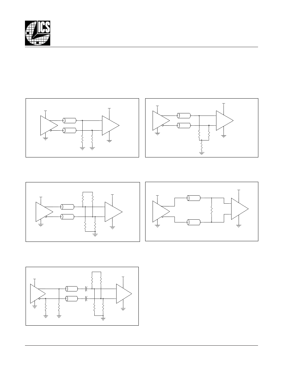
The CLK /nCLK accepts LVDS, LVPECL, LVHSTL, SSTL, HCSL
and other differential signals. Both V
SWING
and V
OH
must meet the
V
PP
and V
CMR
input requirements. Figures 2A to 2E show inter-
face examples for the HiPerClockS CLK/nCLK input driven by
the most common driver types. The input interfaces suggested
F
IGURE
2A. H
I
P
ER
C
LOCK
S CLK/nCLK I
NPUT
D
RIVEN
BY
ICS H
I
P
ER
C
LOCK
S LVHSTL D
RIVER
here are examples only. Please consult with the vendor of the
driver component to confirm the driver termination requirements.
For example in
Figure 2A,
the input termination applies for ICS
HiPerClockS LVHSTL drivers. If you are using an LVHSTL driver
from another vendor, use their termination recommendation.
1.8V
R2
50
Input
LVHSTL Driver
ICS
HiPerClockS
R1
50
LVHSTL
3.3V
Zo = 50 Ohm
Zo = 50 Ohm
HiPerClockS
CLK
nCLK
F
IGURE
2E. H
I
P
ER
C
LOCK
S CLK/
N
CLK I
NPUT
D
RIVEN
BY
3.3V LVPECL D
RIVER
WITH
AC C
OUPLE
Zo = 50 Ohm
R3
125
HiPerClockS
CLK
nCLK
3.3V
R5
100 - 200
3.3V
R2
84
3.3V
R6
100 - 200
Input
R5,R6 locate near the driver pin.
Zo = 50 Ohm
R1
84
R4
125
C2
LVPECL
C1
Zo = 50 Ohm
R1
100
3.3V
LVDS_Driv er
Zo = 50 Ohm
Receiv er
CLK
nCLK
3.3V

8516FY
www.icst.com/products/hiperclocks.html
REV. B FEBRUARY 21, 2006
11
Integrated
Circuit
Systems, Inc.
ICS8516
L
OW
S
KEW
, 1-
TO
-16
D
IFFERENTIAL
-
TO
-LVDS C
LOCK
D
ISTRIBUTION
C
HIP
LVDS D
RIVER
T
ERMINATION
A general LVDS interface is shown in
Figure 3.
In a 100
differential transmission line environment, LVDS drivers re-
quire a matched load termination of 100
across near the
receiver input. For a multiple LVDS outputs buffer, if only par-
tial outputs are used, it is recommended to terminate the un-
used outputs.
F
IGURE
3. T
YPICAL
LVDS D
RIVER
T
ERMINATION
3.3V
R1
100
Zo = 50 Ohm
LVDS_Driver
HiPerClockS
CLK
nCLK
Zo = 50 Ohm
3.3V
F
IGURE
4. ICS8516 LVDS B
UFFER
S
CHEMATIC
E
XAMPLE
C5
0.1u
(U1-12)
Zo = 50 Ohm
Zo = 50 Ohm
(U1-25)
LVDS_input
+
-
(U1-31)
Zo = 50 Ohm
C3
0.1u
C6
0.1u
U1
8516
1
2
3
4
5
6
7
8
9
10
11
12
13
14
15
16
17
18
19
20
21
22
23
24
36
35
34
33
32
31
30
29
28
27
26
25
48
47
46
45
44
43
42
41
40
39
38
37
VD
D
nQ
5
Q5
nQ
4
Q4
VD
D
GND
nQ
3
Q3
nQ
2
Q2
VD
D
nQ1
Q1
nQ0
Q0
GND
nCLK
CLK
GND
Q15
nQ15
Q14
nQ14
VD
D
nQ
10
Q1
0
nQ
11
Q1
1
VD
D
GND
nQ
12
Q1
2
nQ
13
Q1
3
VD
D
Q6
nQ6
Q7
nQ7
GND
OE1
OE2
GND
nQ8
Q8
nQ9
Q9
Zo = 50 Ohm
R16
100
Zo = 50 Ohm
VDD=3.3V
LVDS_input
+
-
Zo = 50 Ohm
Zo = 50 Ohm
Zo = 50 Ohm
VDD=3.3V
R10
100
C4
0.1u
C2
0.1u
LVDS_Driver
R17
100
LVDS_input
+
-
(U1-1)
Decoupling capacitors located near the power pins
(U1-6)
(U1-36)
R1
100
C1
0.1u
S
CHEMATIC
E
XAMPLE
Figure 4
shows a schematic example of ICS8516. In this ex-
ample, the input is driven by an LVDS driver. For LVDS buffer,
it is recommended to terminate the unused outputs for better
signal integrity. The decoupling capacitors should be physi-
cally located near the power pin.

8516FY
www.icst.com/products/hiperclocks.html
REV. B FEBRUARY 21, 2006
12
Integrated
Circuit
Systems, Inc.
ICS8516
L
OW
S
KEW
, 1-
TO
-16
D
IFFERENTIAL
-
TO
-LVDS C
LOCK
D
ISTRIBUTION
C
HIP
R
ELIABILITY
I
NFORMATION
T
RANSISTOR
C
OUNT
The transistor count for ICS8516 is: 1821
T
ABLE
6.
JA
VS
. A
IR
F
LOW
T
ABLE
FOR
48 L
EAD
LQFP
JA
by Velocity (Linear Feet per Minute)
0
200
500
Single-Layer PCB, JEDEC Standard Test Boards
67.8∞C/W
55.9∞C/W
50.1∞C/W
Multi-Layer PCB, JEDEC Standard Test Boards
47.9∞C/W
42.1∞C/W
39.4∞C/W
NOTE: Most modern PCB designs use multi-layered boards. The data in the second row pertains to most designs.

8516FY
www.icst.com/products/hiperclocks.html
REV. B FEBRUARY 21, 2006
13
Integrated
Circuit
Systems, Inc.
ICS8516
L
OW
S
KEW
, 1-
TO
-16
D
IFFERENTIAL
-
TO
-LVDS C
LOCK
D
ISTRIBUTION
C
HIP
T
ABLE
7. P
ACKAGE
D
IMENSIONS
N
O
I
T
A
I
R
A
V
C
E
D
E
J
S
R
E
T
E
M
I
L
L
I
M
N
I
S
N
O
I
S
N
E
M
I
D
L
L
A
L
O
B
M
Y
S
C
B
B
M
U
M
I
N
I
M
L
A
N
I
M
O
N
M
U
M
I
X
A
M
N
8
4
A
-
-
-
-
0
6
.
1
1
A
5
0
.
0
-
-
5
1
.
0
2
A
5
3
.
1
0
4
.
1
5
4
.
1
b
7
1
.
0
2
2
.
0
7
2
.
0
c
9
0
.
0
-
-
0
2
.
0
D
C
I
S
A
B
0
0
.
9
1
D
C
I
S
A
B
0
0
.
7
2
D
.
f
e
R
0
5
.
5
E
C
I
S
A
B
0
0
.
9
1
E
C
I
S
A
B
0
0
.
7
2
E
.
f
e
R
0
5
.
5
e
C
I
S
A
B
0
5
.
0
L
5
4
.
0
0
6
.
0
5
7
.
0
0
∞
-
-
7
∞
c
c
c
-
-
-
-
8
0
.
0
Reference Document: JEDEC Publication 95, MS-026
P
ACKAGE
O
UTLINE
- Y S
UFFIX
FOR
48 L
EAD
LQFP

