Document Outline
- General Description
- Features
- Block Diagram
- Pin Assignment
- Pin Descriptions
- Pin Characteristics
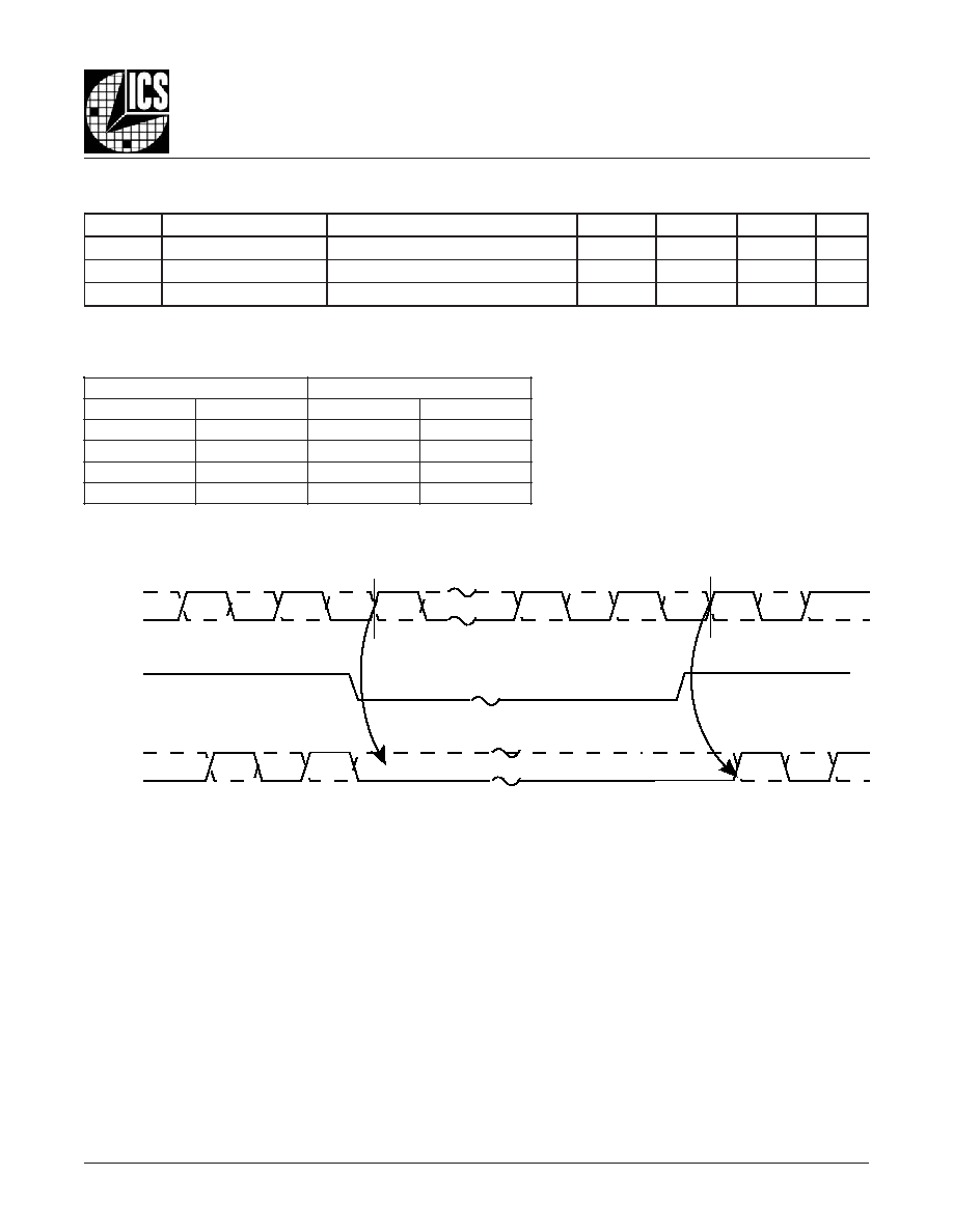
- Control Input Function Table
- OE Timing Diagram
- Absolute Maximum Ratings
- Power Supply DC Characteristics
- LVCMOS DC Characteristics
- Differential DC Characteristics
- LVPECL DC Characteristics
- HSTL DC Characteristics
- AC Characteristics
- Additive Phase Jitter
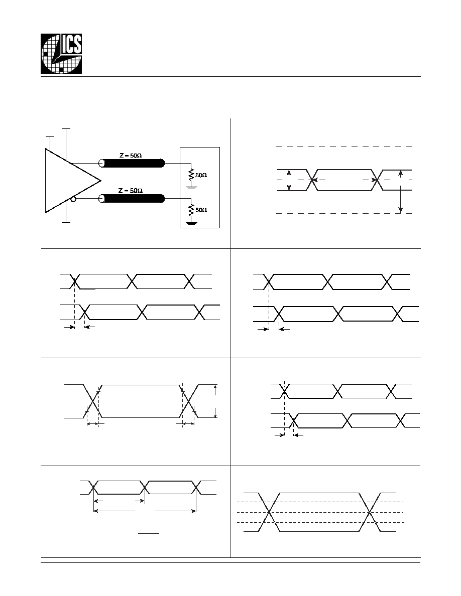
- Parameter Measurement Information
- 3.3V Core/1.8V Output Load AC Test Circuit Diagram
- Differential Input Level Diagram
- Part-to-Part Skew Diagram
- Output Skew Diagram
- Output Rise/Fall Time Diagram
- Propagation Delay Diagram
- Output Duty Cycle/Pulse Width/Period Diagram
- Output Crossover Voltage Diagram
- Application Information
- Wiring the Differential Input to Accept Single Ended Levels
- Differential Clock Input Interface
- HiPerClockS CLK/nCLK Input Driven by ICS HiPerClockS HSTL Driver Diagram
- HiPerClockS CLK/nCLK Input Driven by 3.3V LVPECL Driver Diagrams
- HiPerClockS CLK/nCLK Input Driven by 3.3V LVDS Driver Diagram
- HiPerClockS CLK/nCLK Input Driven by 3.3V LVPECL Driver w/AC Couple Diagram
- LVPECL Clock Input Interface
- HiPerClockS PCLK/nPCLK Input Driven by a CML Driver Diagram
- HiPerClockS PCLK/nPCLK Input Driven by an SSTL Driver Diagram
- HiPerClockS PCLK/nPCLK Input Driven by a 3.3V LVPECL Driver Diagram
- HiPerClockS PCLK/nPCLK Input Driven by a 3.3V LVDS Driver Diagram
- HiPerClockS PCLK/nPCLK Input Driven by a 3.3V LVPECL Driver w/AC Couple Diagram
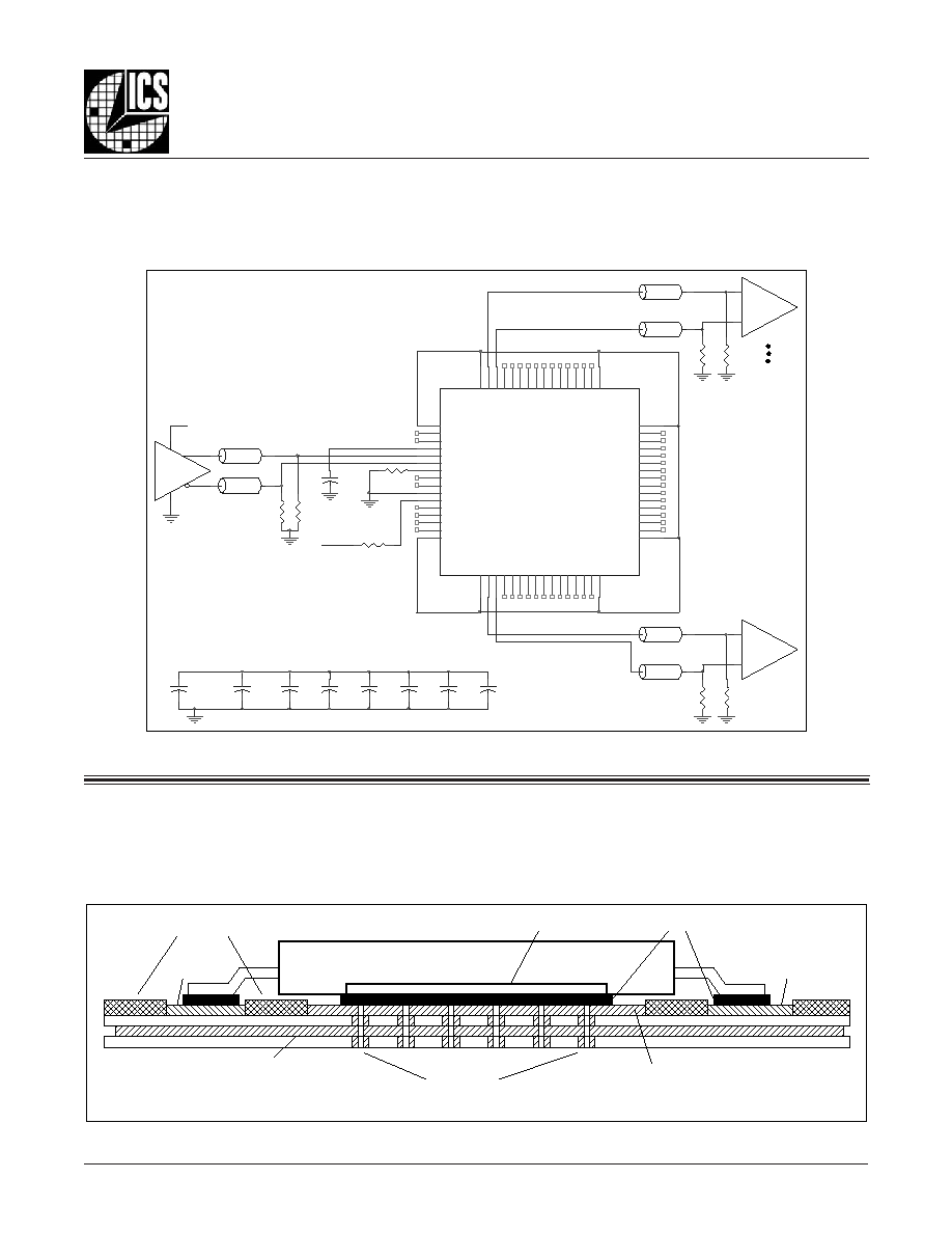
- Schematic Example
- Thermal Release Path
- Power Considerations
- Power Dissipation
- Junciton Temperature
- Thermal Resistance
- Calculations & Equations
- HSTL Driver Circuit & Termination Diagram
- Reliability Information
- Transistor Count
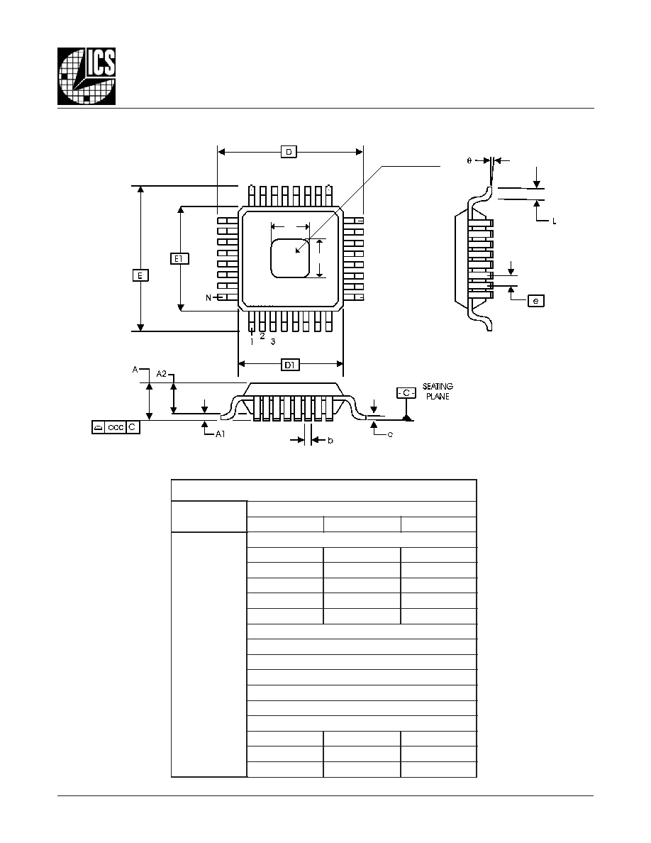
- Package Outline
- Package Dimensions
- Ordering Information
- Revision History Sheet

8524AY
www.icst.com/products/hiperclocks.html
REV. B SEPTEMBER 18, 2003
1
Integrated
Circuit
Systems, Inc.
ICS8524
L
OW
S
KEW
, 1-
TO
-22
D
IFFERENTIAL
-
TO
-HSTL F
ANOUT
B
UFFER
G
ENERAL
D
ESCRIPTION
The ICS8524 is a low skew, 1-to-22 Differential-
to-HSTL Fanout Buffer and a member of the
HiPerClockSTM Family of High Performance Clock
Solutions from ICS. The ICS8524 has two select-
able clock inputs. The CLK, nCLK pair can accept
most standard differential input levels. The PCLK, nPCLK pair
can accept LVPECL, CML, or SSTL input levels. The device is
internally synchronized to eliminate runt pulses on the outputs
during asynchronous assertion/deassertion of the OE pin. The
ICS8524's low output and part-to-part skew characteristics
make it ideal for workstation, server, and other high performance
clock distribution applications.
F
EATURES
� 22 differential HSTL outputs
each with the ability to drive 50
to ground
� Selectable differential CLK, nCLK or LVPECL clock inputs
� CLK, nCLK pair can accept the following differential
input levels: LVPECL, LVDS, HSTL, SSTL, HCSL
� PCLK, nPCLK supports the following input types:
LVPECL, CML, SSTL
� Maximum output frequency: 500MHz
� Translates any single-ended input signal (LVCMOS, LVTTL,
GTL) to HSTL levels with resistor bias on nCLK input
� Output skew: 80ps (maximum)
� Part-to-part skew: 700ps (maximum)
� Jitter, RMS: 0.04ps (typical)
� LVPECL and HSTL mode operating voltage supply range: V
DD
= 3.3V � 5%, V
DDO
= 1.6V to 2V, GND = 0V
� 0�C to 85�C ambient operating temperature
� Pin compatible with the SY89824L and NB100EP223
B
LOCK
D
IAGRAM
P
IN
A
SSIGNMENT
HiPerClockSTM
ICS
CLK
nCLK
PCLK
nPCLK
Q0:Q21
nQ0:nQ21
LE
Q
D
CLK_SEL
OE
0
1
22
22
64-Lead TQFP E-Pad
10mm x 10mm x 1.0mm package body
Y package
Top View
48 47 46 45 44 43 42 41 40 39 38 37 36 35 34 33
1 2 3 4 5 6 7 8 9 10 11 12 13 14 15 16
49
50
51
52
53
54
55
56
57
58
59
60
61
62
63
64
32
31
30
29
28
27
26
25
24
23
22
21
20
19
18
17
ICS8524
V
DDO
Q14
nQ14
Q15
nQ15
Q16
nQ16
Q17
nQ17
Q18
nQ18
Q19
nQ19
Q20
nQ20
V
DDO
V
DDO
nQ6
Q6
nQ5
Q5
nQ4
Q4
nQ3
Q3
nQ2
Q2
nQ1
Q1
nQ0
Q0
V
DDO
V
DDO
nQ13
Q13
nQ12
Q12
nQ11
Q11
nQ10
Q10
nQ9
Q9
nQ8
Q8
nQ7
Q7
V
DDO
V
DDO
nc
nc
V
DD
CLK
nCLK
CLK_SEL
PCLK
nPCLK
GND
OE
nc
nc
nQ21
Q21
V
DDO

8524AY
www.icst.com/products/hiperclocks.html
REV. B SEPTEMBER 18, 2003
2
Integrated
Circuit
Systems, Inc.
ICS8524
L
OW
S
KEW
, 1-
TO
-22
D
IFFERENTIAL
-
TO
-HSTL F
ANOUT
B
UFFER
T
ABLE
1. P
IN
D
ESCRIPTIONS
r
e
b
m
u
N
e
m
a
N
e
p
y
T
n
o
i
t
p
i
r
c
s
e
D
,
2
3
,
7
1
,
6
1
,
1
4
6
,
9
4
,
8
4
,
3
3
V
O
D
D
r
e
w
o
P
.
s
n
i
p
y
l
p
p
u
s
t
u
p
t
u
O
3
1
,
2
1
,
3
,
2
c
n
d
e
s
u
n
U
.
t
c
e
n
n
o
c
o
N
4
V
D
D
r
e
w
o
P
.
n
i
p
y
l
p
p
u
s
e
r
o
C
5
K
L
C
t
u
p
n
I
n
w
o
d
ll
u
P
.
r
i
a
p
t
u
p
n
i
k
c
o
l
c
l
a
i
t
n
e
r
e
f
f
i
d
g
n
i
t
r
e
v
n
i
-
n
o
N
6
K
L
C
n
t
u
p
n
I
/
p
u
ll
u
P
n
w
o
d
ll
u
P
o
t
d
e
s
a
i
B
.
r
i
a
p
t
u
p
n
i
k
c
o
l
c
l
a
i
t
n
e
r
e
f
f
i
d
g
n
i
t
r
e
v
n
I
2
/
3
V
C
C
.
7
L
E
S
_
K
L
C
t
u
p
n
I
p
u
ll
u
P
.
s
t
u
p
n
i
K
L
C
P
n
,
K
L
C
P
s
t
c
e
l
e
s
,
H
G
I
H
n
e
h
W
.
t
u
p
n
i
t
c
e
l
e
s
k
c
o
l
C
.
s
t
u
p
n
i
K
L
C
n
,
K
L
C
s
t
c
e
l
e
s
,
W
O
L
n
e
h
W
.
s
l
e
v
e
l
e
c
a
f
r
e
t
n
i
L
T
T
V
L
/
S
O
M
C
V
L
8
K
L
C
P
t
u
p
n
I
n
w
o
d
ll
u
P
.
r
i
a
p
t
u
p
n
i
k
c
o
l
c
L
C
E
P
V
L
l
a
i
t
n
e
r
e
f
f
i
d
g
n
i
t
r
e
v
n
i
-
n
o
N
9
K
L
C
P
n
t
u
p
n
I
/
p
u
ll
u
P
n
w
o
d
ll
u
P
o
t
d
e
s
a
i
B
.
r
i
a
p
t
u
p
n
i
k
c
o
l
c
L
C
E
P
V
L
l
a
i
t
n
e
r
e
f
f
i
d
g
n
i
t
r
e
v
n
I
2
/
3
V
C
C
.
0
1
D
N
G
r
e
w
o
P
.
d
n
u
o
r
g
y
l
p
p
u
s
r
e
w
o
P
1
1
E
O
t
u
p
n
I
p
u
ll
u
P
s
t
u
p
t
u
o
f
o
g
n
il
b
a
s
i
d
d
n
a
g
n
il
b
a
n
e
s
l
o
r
t
n
o
C
.
e
l
b
a
n
e
t
u
p
t
u
O
.
s
l
e
v
e
l
e
c
a
f
r
e
t
n
i
L
T
T
V
L
/
S
O
M
C
V
L
.
1
2
Q
n
:
0
Q
n
,
1
2
Q
:
0
Q
5
1
,
4
1
1
2
Q
,
1
2
Q
n
t
u
p
t
u
O
.
s
l
e
v
e
l
e
c
a
f
r
e
t
n
i
L
T
S
H
.
s
t
u
p
t
u
o
k
c
o
l
c
l
a
i
t
n
e
r
e
f
f
i
D
9
1
,
8
1
0
2
Q
,
0
2
Q
n
t
u
p
t
u
O
.
s
l
e
v
e
l
e
c
a
f
r
e
t
n
i
L
T
S
H
.
s
t
u
p
t
u
o
k
c
o
l
c
l
a
i
t
n
e
r
e
f
f
i
D
1
2
,
0
2
9
1
Q
,
9
1
Q
n
t
u
p
t
u
O
.
s
l
e
v
e
l
e
c
a
f
r
e
t
n
i
L
T
S
H
.
s
t
u
p
t
u
o
k
c
o
l
c
l
a
i
t
n
e
r
e
f
f
i
D
3
2
,
2
2
8
1
Q
,
8
1
Q
n
t
u
p
t
u
O
.
s
l
e
v
e
l
e
c
a
f
r
e
t
n
i
L
T
S
H
.
s
t
u
p
t
u
o
k
c
o
l
c
l
a
i
t
n
e
r
e
f
f
i
D
5
2
,
4
2
7
1
Q
,
7
1
Q
n
t
u
p
t
u
O
.
s
l
e
v
e
l
e
c
a
f
r
e
t
n
i
L
T
S
H
.
s
t
u
p
t
u
o
k
c
o
l
c
l
a
i
t
n
e
r
e
f
f
i
D
7
2
,
6
2
6
1
Q
,
6
1
Q
n
t
u
p
t
u
O
.
s
l
e
v
e
l
e
c
a
f
r
e
t
n
i
L
T
S
H
.
s
t
u
p
t
u
o
k
c
o
l
c
l
a
i
t
n
e
r
e
f
f
i
D
9
2
,
8
2
5
1
Q
,
5
1
Q
n
t
u
p
t
u
O
.
s
l
e
v
e
l
e
c
a
f
r
e
t
n
i
L
T
S
H
.
s
t
u
p
t
u
o
k
c
o
l
c
l
a
i
t
n
e
r
e
f
f
i
D
1
3
,
0
3
4
1
Q
,
4
1
Q
n
t
u
p
t
u
O
.
s
l
e
v
e
l
e
c
a
f
r
e
t
n
i
L
T
S
H
.
s
t
u
p
t
u
o
k
c
o
l
c
l
a
i
t
n
e
r
e
f
f
i
D
5
3
,
4
3
3
1
Q
,
3
1
Q
n
t
u
p
t
u
O
.
s
l
e
v
e
l
e
c
a
f
r
e
t
n
i
L
T
S
H
.
s
t
u
p
t
u
o
k
c
o
l
c
l
a
i
t
n
e
r
e
f
f
i
D
7
3
,
6
3
2
1
Q
,
2
1
Q
n
t
u
p
t
u
O
.
s
l
e
v
e
l
e
c
a
f
r
e
t
n
i
L
T
S
H
.
s
t
u
p
t
u
o
k
c
o
l
c
l
a
i
t
n
e
r
e
f
f
i
D
9
3
,
8
3
1
1
Q
,
1
1
Q
n
t
u
p
t
u
O
.
s
l
e
v
e
l
e
c
a
f
r
e
t
n
i
L
T
S
H
.
s
t
u
p
t
u
o
k
c
o
l
c
l
a
i
t
n
e
r
e
f
f
i
D
1
4
,
0
4
0
1
Q
,
0
1
Q
n
t
u
p
t
u
O
.
s
l
e
v
e
l
e
c
a
f
r
e
t
n
i
L
T
S
H
.
s
t
u
p
t
u
o
k
c
o
l
c
l
a
i
t
n
e
r
e
f
f
i
D
3
4
,
2
4
9
Q
,
9
Q
n
t
u
p
t
u
O
.
s
l
e
v
e
l
e
c
a
f
r
e
t
n
i
L
T
S
H
.
s
t
u
p
t
u
o
k
c
o
l
c
l
a
i
t
n
e
r
e
f
f
i
D
5
4
,
4
4
8
Q
,
8
Q
n
t
u
p
t
u
O
.
s
l
e
v
e
l
e
c
a
f
r
e
t
n
i
L
T
S
H
.
s
t
u
p
t
u
o
k
c
o
l
c
l
a
i
t
n
e
r
e
f
f
i
D
7
4
,
6
4
7
Q
,
7
Q
n
t
u
p
t
u
O
.
s
l
e
v
e
l
e
c
a
f
r
e
t
n
i
L
T
S
H
.
s
t
u
p
t
u
o
k
c
o
l
c
l
a
i
t
n
e
r
e
f
f
i
D
1
5
,
0
5
6
Q
,
6
Q
n
t
u
p
t
u
O
.
s
l
e
v
e
l
e
c
a
f
r
e
t
n
i
L
T
S
H
.
s
t
u
p
t
u
o
k
c
o
l
c
l
a
i
t
n
e
r
e
f
f
i
D
3
5
,
2
5
5
Q
,
5
Q
n
t
u
p
t
u
O
.
s
l
e
v
e
l
e
c
a
f
r
e
t
n
i
L
T
S
H
.
s
t
u
p
t
u
o
k
c
o
l
c
l
a
i
t
n
e
r
e
f
f
i
D
5
5
,
4
5
4
Q
,
4
Q
n
t
u
p
t
u
O
.
s
l
e
v
e
l
e
c
a
f
r
e
t
n
i
L
T
S
H
.
s
t
u
p
t
u
o
k
c
o
l
c
l
a
i
t
n
e
r
e
f
f
i
D
7
5
,
6
5
3
Q
,
3
Q
n
t
u
p
t
u
O
.
s
l
e
v
e
l
e
c
a
f
r
e
t
n
i
L
T
S
H
.
s
t
u
p
t
u
o
k
c
o
l
c
l
a
i
t
n
e
r
e
f
f
i
D
9
5
,
8
5
2
Q
,
2
Q
n
t
u
p
t
u
O
.
s
l
e
v
e
l
e
c
a
f
r
e
t
n
i
L
T
S
H
.
s
t
u
p
t
u
o
k
c
o
l
c
l
a
i
t
n
e
r
e
f
f
i
D
1
6
,
0
6
1
Q
,
1
Q
n
t
u
p
t
u
O
.
s
l
e
v
e
l
e
c
a
f
r
e
t
n
i
L
T
S
H
.
s
t
u
p
t
u
o
k
c
o
l
c
l
a
i
t
n
e
r
e
f
f
i
D
3
6
,
2
6
0
Q
,
0
Q
n
t
u
p
t
u
O
.
s
l
e
v
e
l
e
c
a
f
r
e
t
n
i
L
T
S
H
.
s
t
u
p
t
u
o
k
c
o
l
c
l
a
i
t
n
e
r
e
f
f
i
D
:
E
T
O
N
p
u
ll
u
P
d
n
a
n
w
o
d
ll
u
P
.
s
e
u
l
a
v
l
a
c
i
p
y
t
r
o
f
,
s
c
i
t
s
i
r
e
t
c
a
r
a
h
C
n
i
P
,
2
e
l
b
a
T
e
e
S
.
s
r
o
t
s
i
s
e
r
t
u
p
n
i
l
a
n
r
e
t
n
i
o
t
r
e
f
e
r
8524AY
www.icst.com/products/hiperclocks.html
REV. B SEPTEMBER 18, 2003
3
Integrated
Circuit
Systems, Inc.
ICS8524
L
OW
S
KEW
, 1-
TO
-22
D
IFFERENTIAL
-
TO
-HSTL F
ANOUT
B
UFFER
T
ABLE
3A. C
ONTROL
I
NPUT
F
UNCTION
T
ABLE
T
ABLE
2. P
IN
C
HARACTERISTICS
l
o
b
m
y
S
r
e
t
e
m
a
r
a
P
s
n
o
i
t
i
d
n
o
C
t
s
e
T
m
u
m
i
n
i
M
l
a
c
i
p
y
T
m
u
m
i
x
a
M
s
t
i
n
U
C
N
I
e
c
n
a
t
i
c
a
p
a
C
t
u
p
n
I
4
F
p
R
P
U
L
L
U
P
r
o
t
s
i
s
e
R
p
u
ll
u
P
t
u
p
n
I
7
3
K
R
N
W
O
D
L
L
U
P
r
o
t
s
i
s
e
R
n
w
o
d
ll
u
P
t
u
p
n
I
5
7
K
s
t
u
p
n
I
s
t
u
p
t
u
O
E
O
L
E
S
_
K
L
C
1
2
Q
:
0
Q
1
2
Q
n
:
0
Q
n
0
0
W
O
L
H
G
I
H
0
1
W
O
L
H
G
I
H
1
0
K
L
C
K
L
C
n
1
1
K
L
C
P
K
L
C
P
n
Enabled
Disabled
F
IGURE
1. OE T
IMING
D
IAGRAM
nCLK,
nPCLK
CLK,PCLK
OE
nQ0 :nQ21
Q0 :Q21
8524AY
www.icst.com/products/hiperclocks.html
REV. B SEPTEMBER 18, 2003
4
Integrated
Circuit
Systems, Inc.
ICS8524
L
OW
S
KEW
, 1-
TO
-22
D
IFFERENTIAL
-
TO
-HSTL F
ANOUT
B
UFFER
T
ABLE
4A. P
OWER
S
UPPLY
DC C
HARACTERISTICS
,
V
DD
= 3.3V�5%, V
DDO
= 1.8V�0.2V, T
A
=0�C
TO
85�C
T
ABLE
4B. LVCMOS / LVTTL DC C
HARACTERISTICS
,
V
DD
= 3.3V�5%, V
DDO
= 1.8V�0.2V, T
A
=0�C
TO
85�C
T
ABLE
4C. D
IFFERENTIAL
DC C
HARACTERISTICS
,
V
DD
= 3.3V�5%, V
DDO
= 1.8V�0.2V, T
A
=0�C
TO
85�C
l
o
b
m
y
S
r
e
t
e
m
a
r
a
P
s
n
o
i
t
i
d
n
o
C
t
s
e
T
m
u
m
i
n
i
M
l
a
c
i
p
y
T
m
u
m
i
x
a
M
s
t
i
n
U
V
D
D
e
g
a
t
l
o
V
y
l
p
p
u
S
e
r
o
C
5
3
1
.
3
3
.
3
5
6
4
.
3
V
V
O
D
D
e
g
a
t
l
o
V
y
l
p
p
u
S
r
e
w
o
P
t
u
t
p
u
O
6
.
1
8
.
1
0
.
2
V
I
D
D
t
n
e
r
r
u
C
y
l
p
p
u
S
e
v
i
t
i
s
o
P
0
2
2
A
m
I
O
D
D
t
n
e
r
r
u
C
y
l
p
p
u
S
t
u
p
t
u
O
d
a
o
L
o
N
1
A
m
l
o
b
m
y
S
r
e
t
e
m
a
r
a
P
s
n
o
i
t
i
d
n
o
C
t
s
e
T
m
u
m
i
n
i
M
l
a
c
i
p
y
T
m
u
m
i
x
a
M
s
t
i
n
U
V
H
I
e
g
a
t
l
o
V
h
g
i
H
t
u
p
n
I
2
V
D
D
3
.
0
+
V
V
L
I
e
g
a
t
l
o
V
w
o
L
t
u
p
n
I
3
.
0
-
8
.
0
V
I
H
I
t
n
e
r
r
u
C
h
g
i
H
t
u
p
n
I
L
E
S
_
K
L
C
,
E
O
5
A
�
I
L
I
t
n
e
r
r
u
C
w
o
L
t
u
p
n
I
L
E
S
_
K
L
C
,
E
O
0
5
1
-
A
�
l
o
b
m
y
S
r
e
t
e
m
a
r
a
P
s
n
o
i
t
i
d
n
o
C
t
s
e
T
m
u
m
i
n
i
M
l
a
c
i
p
y
T
m
u
m
i
x
a
M
s
t
i
n
U
I
H
I
t
n
e
r
r
u
C
h
g
i
H
t
u
p
n
I
K
L
C
n
,
K
L
C
V
D
D
V
=
N
I
V
5
6
4
.
3
=
0
5
1
A
�
I
L
I
t
n
e
r
r
u
C
w
o
L
t
u
p
n
I
K
L
C
n
,
K
L
C
V
D
D
V
,
V
5
6
4
.
3
=
N
I
V
0
=
0
5
1
-
A
�
V
P
P
e
g
a
t
l
o
V
t
u
p
n
I
k
a
e
P
-
o
t
-
k
a
e
P
5
1
.
0
3
.
1
V
V
R
M
C
2
,
1
E
T
O
N
;
e
g
a
t
l
o
V
t
u
p
n
I
e
d
o
M
n
o
m
m
o
C
5
.
0
+
D
N
G
V
D
D
5
8
.
0
-
V
V
s
a
d
e
n
i
f
e
d
s
i
e
g
a
t
l
o
v
e
d
o
m
n
o
m
m
o
C
:
1
E
T
O
N
H
I
.
V
s
i
K
L
C
n
d
n
a
K
L
C
r
o
f
e
g
a
t
l
o
v
t
u
p
n
i
m
u
m
i
x
a
m
e
h
t
,
s
n
o
i
t
a
c
il
p
p
a
d
e
d
n
e
e
l
g
n
i
s
r
o
F
:
2
E
T
O
N
D
D
.
V
3
.
0
+
NOTE: Stresses beyond those listed under Absolute
Maximum Ratings may cause permanent damage to the
device. These ratings are stress specifications only. Functional
operation of product at these conditions or any conditions be-
yond those listed in the
DC Characteristics or AC Character-
istics is not implied. Exposure to absolute maximum rating
conditions for extended periods may affect product reliability.
A
BSOLUTE
M
AXIMUM
R
ATINGS
Supply Voltage, V
DD
4.6V
Inputs, V
I
-0.5V to V
DD
+ 0.5V
Outputs, I
O
Continuous Current
50mA
Surge Current
100mA
Package Thermal Impedance,
JA
22.3�C/W (0 lfpm)
Storage Temperature, T
STG
-65�C to 150�C
8524AY
www.icst.com/products/hiperclocks.html
REV. B SEPTEMBER 18, 2003
5
Integrated
Circuit
Systems, Inc.
ICS8524
L
OW
S
KEW
, 1-
TO
-22
D
IFFERENTIAL
-
TO
-HSTL F
ANOUT
B
UFFER
T
ABLE
5. AC C
HARACTERISTICS
,
V
DD
= 3.3V�5%, V
DDO
= 1.8V�0.2V, T
A
=0�C
TO
85�C
T
ABLE
4D. LVPECL DC C
HARACTERISTICS
,
V
DD
= 3.3V�5%, V
DDO
= 1.8V�0.2V, T
A
=0�C
TO
85�C
l
o
b
m
y
S
r
e
t
e
m
a
r
a
P
s
n
o
i
t
i
d
n
o
C
t
s
e
T
m
u
m
i
n
i
M
l
a
c
i
p
y
T
m
u
m
i
x
a
M
s
t
i
n
U
I
H
I
t
n
e
r
r
u
C
h
g
i
H
t
u
p
n
I
K
L
C
P
n
,
K
L
C
P
V
D
D
V
=
N
I
V
5
6
4
.
3
=
0
5
1
A
�
I
L
I
t
n
e
r
r
u
C
w
o
L
t
u
p
n
I
K
L
C
P
n
,
K
L
C
P
V
D
D
V
,
V
5
6
4
.
3
=
N
I
V
0
=
0
5
1
-
A
�
V
P
P
e
g
a
t
l
o
V
t
u
p
n
I
k
a
e
P
-
o
t
-
k
a
e
P
3
.
0
1
V
V
R
M
C
2
,
1
E
T
O
N
;
e
g
a
t
l
o
V
t
u
p
n
I
e
d
o
M
n
o
m
m
o
C
5
.
1
+
D
N
G
V
D
D
V
V
s
a
d
e
n
i
f
e
d
s
i
e
g
a
t
l
o
v
e
d
o
m
n
o
m
m
o
C
:
1
E
T
O
N
H
I
.
V
s
i
K
L
C
P
n
d
n
a
K
L
C
P
r
o
f
e
g
a
t
l
o
v
t
u
p
n
i
m
u
m
i
x
a
m
e
h
t
,
s
n
o
i
t
a
c
il
p
p
a
d
e
d
n
e
e
l
g
n
i
s
r
o
F
:
2
E
T
O
N
D
D
.
V
3
.
0
+
l
o
b
m
y
S
r
e
t
e
m
a
r
a
P
s
n
o
i
t
i
d
n
o
C
t
s
e
T
m
u
m
i
n
i
M
l
a
c
i
p
y
T
m
u
m
i
x
a
M
s
t
i
n
U
f
X
A
M
y
c
n
e
u
q
e
r
F
t
u
p
t
u
O
0
0
5
z
H
M
t
D
P
1
E
T
O
N
;
y
a
l
e
D
n
o
i
t
a
g
a
p
o
r
P
7
.
1
7
.
2
s
n
t
)
o
(
k
s
4
,
2
E
T
O
N
;
w
e
k
S
t
u
p
t
u
O
0
8
s
p
t
)
p
p
(
k
s
4
,
3
E
T
O
N
;
w
e
k
S
t
r
a
P
-
o
t
-
t
r
a
P
0
0
7
s
p
t t
ij
;
S
M
R
,
r
e
t
t
i
J
e
s
a
h
P
e
v
i
t
i
d
d
A
r
e
f
f
u
B
n
o
i
t
c
e
s
r
e
t
t
i
J
e
s
a
h
P
e
v
i
t
i
d
d
A
o
t
r
e
f
e
r
4
0
.
0
s
p
t
R
t
/
F
e
m
i
T
ll
a
F
/
e
s
i
R
t
u
p
t
u
O
%
0
8
o
t
%
0
2
0
0
3
0
0
7
s
p
t
S
e
m
i
T
p
u
t
e
S
0
.
1
s
n
t
H
e
m
i
T
d
l
o
H
5
.
0
s
n
c
d
o
e
l
c
y
C
y
t
u
D
t
u
p
t
u
O
z
H
M
3
3
1
9
4
1
5
%
<
3
3
1
z
H
M
6
6
2
8
4
2
5
%
.
t
n
i
o
p
g
n
i
s
s
o
r
c
t
u
p
t
u
o
l
a
i
t
n
e
r
e
f
f
i
d
e
h
t
o
t
t
n
i
o
p
g
n
i
s
s
o
r
c
t
u
p
n
i
l
a
i
t
n
e
r
e
f
f
i
d
e
h
t
m
o
r
f
d
e
r
u
s
a
e
M
:
1
E
T
O
N
.
s
n
o
i
t
i
d
n
o
c
d
a
o
l
l
a
u
q
e
h
t
i
w
d
n
a
e
g
a
t
l
o
v
y
l
p
p
u
s
e
m
a
s
e
h
t
t
a
s
t
u
p
t
u
o
n
e
e
w
t
e
b
w
e
k
s
s
a
d
e
n
i
f
e
D
:
2
E
T
O
N
.
s
t
n
i
o
p
s
s
o
r
c
l
a
i
t
n
e
r
e
f
f
i
d
t
u
p
t
u
o
e
h
t
t
a
d
e
r
u
s
a
e
M
s
e
g
a
t
l
o
v
y
l
p
p
u
s
e
m
a
s
e
h
t
t
a
g
n
i
t
a
r
e
p
o
s
e
c
i
v
e
d
t
n
e
r
e
f
f
i
d
n
o
s
t
u
p
t
u
o
n
e
e
w
t
e
b
w
e
k
s
s
a
d
e
n
i
f
e
D
:
3
E
T
O
N
,
e
c
i
v
e
d
h
c
a
e
n
o
s
t
u
p
n
i
f
o
e
p
y
t
e
m
a
s
e
h
t
g
n
i
s
U
.
e
r
u
t
a
r
e
p
m
e
t
e
m
a
s
e
h
t
t
a
s
n
o
i
t
i
d
n
o
c
d
a
o
l
l
a
u
q
e
h
t
i
w
d
n
a
.
s
t
n
i
o
p
s
s
o
r
c
l
a
i
t
n
e
r
e
f
f
i
d
e
h
t
t
a
d
e
r
u
s
a
e
m
e
r
a
s
t
u
p
t
u
o
e
h
t
.
5
6
d
r
a
d
n
a
t
S
C
E
D
E
J
h
t
i
w
e
c
n
a
d
r
o
c
c
a
n
i
d
e
n
i
f
e
d
s
i
r
e
t
e
m
a
r
a
p
s
i
h
T
:
4
E
T
O
N
T
ABLE
4E. HSTL DC C
HARACTERISTICS
,
V
DD
= 3.3V�5%, V
DDO
= 1.8V�0.2V, T
A
=0�C
TO
85�C
l
o
b
m
y
S
r
e
t
e
m
a
r
a
P
s
n
o
i
t
i
d
n
o
C
t
s
e
T
m
u
m
i
n
i
M
l
a
c
i
p
y
T
m
u
m
i
x
a
M
s
t
i
n
U
V
H
O
1
E
T
O
N
;
e
g
a
t
l
o
V
h
g
i
H
t
u
p
t
u
O
0
.
1
4
.
1
V
V
L
O
1
E
T
O
N
;
e
g
a
t
l
o
V
w
o
L
t
u
p
t
u
O
0
4
.
0
V
V
X
O
2
E
T
O
N
;
e
g
a
t
l
o
V
r
e
v
o
s
s
o
r
C
t
u
p
t
u
O
0
4
0
6
%
V
G
N
I
W
S
g
n
i
w
S
e
g
a
t
l
o
V
t
u
p
t
u
O
k
a
e
P
-
o
t
-
k
a
e
P
6
.
0
1
.
1
V
0
5
h
t
i
w
d
e
t
a
n
i
m
r
e
t
s
t
u
p
t
u
O
:
1
E
T
O
N
.
d
n
u
o
r
g
o
t
.
n
o
i
t
i
d
n
o
c
n
e
v
i
g
a
t
a
g
n
i
w
s
e
g
a
t
l
o
v
t
u
p
t
u
o
o
t
t
c
e
p
s
e
r
h
t
i
w
d
e
n
i
f
e
D
:
2
E
T
O
N
8524AY
www.icst.com/products/hiperclocks.html
REV. B SEPTEMBER 18, 2003
6
Integrated
Circuit
Systems, Inc.
ICS8524
L
OW
S
KEW
, 1-
TO
-22
D
IFFERENTIAL
-
TO
-HSTL F
ANOUT
B
UFFER
A
DDITIVE
P
HASE
J
ITTER
Input/Output Additive
Phase Jitter
at 156.25MHz
= 0.04ps (typical)
0
-10
-20
-30
-40
-50
-60
-70
-80
-90
-100
-110
-120
-130
-140
-150
-160
-170
-180
-190
1k
10k
100k
1M
10M
100M
The spectral purity in a band at a specific offset from the funda-
mental compared to the power of the fundamental is called the
dBc Phase Noise. This value is normally expressed using a
Phase noise plot and is most often the specified plot in many
applications. Phase noise is defined as the ratio of the noise
power present in a 1Hz band at a specified offset from the fun-
damental frequency to the power value of the fundamental. This
ratio is expressed in decibels (dBm) or a ratio of the power in
As with most timing specifications, phase noise measurements
have issues. The primary issue relates to the limitations of the
equipment. Often the noise floor of the equipment is higher than
the noise floor of the device. This is illustrated above. The de-
the 1Hz band to the power in the fundamental. When the re-
quired offset is specified, the phase noise is called a
dBc value,
which simply means dBm at a specified offset from the funda-
mental. By investigating jitter in the frequency domain, we get a
better understanding of its effects on the desired application over
the entire time record of the signal. It is mathematically possible
to calculate an expected bit error rate given a phase noise plot.
vice meets the noise floor of what is shown, but can actually be
lower. The phase noise is dependant on the input source and
measurement equipment.
O
FFSET
F
ROM
C
ARRIER
F
REQUENCY
(H
Z
)
SSB P
HASE
N
OISE
dBc/H
Z
8524AY
www.icst.com/products/hiperclocks.html
REV. B SEPTEMBER 18, 2003
7
Integrated
Circuit
Systems, Inc.
ICS8524
L
OW
S
KEW
, 1-
TO
-22
D
IFFERENTIAL
-
TO
-HSTL F
ANOUT
B
UFFER
P
ARAMETER
M
EASUREMENT
I
NFORMATION
3.3V C
ORE
/1.8V O
UTPUT
L
OAD
AC T
EST
C
IRCUIT
D
IFFERENTIAL
I
NPUT
L
EVEL
O
UTPUT
S
KEW
t
sk(o)
nQx
Qx
nQy
nQy
P
ART
-
TO
-P
ART
S
KEW
tsk(pp)
nQx
Qx
nQy
Qy
PART 1
PART 2
O
UTPUT
R
ISE
/F
ALL
T
IME
SCOPE
HSTL
Qx
nQx
V
CMR
Cross Points
V
PP
V
DD
GND
nCLK, nPCLK
CLK, PCLK
0V
3.3V�5%
V
DD
V
DDO
1.8V�0.2V
O
UTPUT
D
UTY
C
YCLE
/P
ULSE
W
IDTH
/P
ERIOD
Pulse Width
t
PERIOD
t
PW
t
PERIOD
odc =
nQ0:nQ21
Q0:Q21
P
ROPAGATION
D
ELAY
nCLK, nPCLK
CLK, PCLK
nQ0:nQ21
Q0:Q21
t
PD
Clock
Outputs
20%
80%
80%
20%
t
R
t
F
V
SW I N G
GND
O
UTPUT
C
ROSSOVER
V
OLTAGE
60%
50%
VOX
40%
8524AY
www.icst.com/products/hiperclocks.html
REV. B SEPTEMBER 18, 2003
8
Integrated
Circuit
Systems, Inc.
ICS8524
L
OW
S
KEW
, 1-
TO
-22
D
IFFERENTIAL
-
TO
-HSTL F
ANOUT
B
UFFER
A
PPLICATION
I
NFORMATION
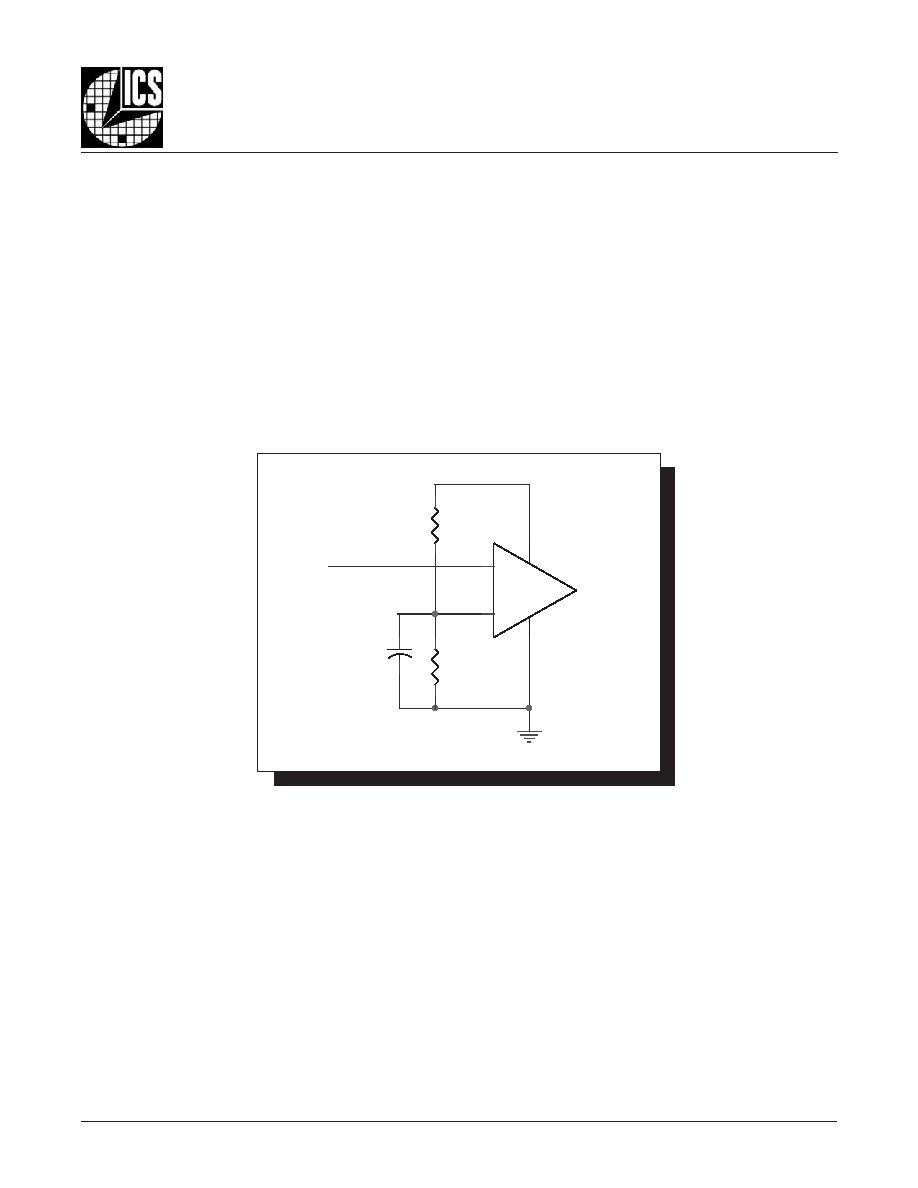
Figure 2 shows how the differential input can be wired to accept
single ended levels. The reference voltage V_REF = V
DD
/2 is
generated by the bias resistors R1, R2 and C1. This bias circuit
should be located as close as possible to the input pin. The ratio
F
IGURE
2. S
INGLE
E
NDED
S
IGNAL
D
RIVING
D
IFFERENTIAL
I
NPUT
R2
1K
V
DD
CLK_IN
+
-
R1
1K
C1
0.1uF
V_REF
W
IRING
THE
D
IFFERENTIAL
I
NPUT
TO
A
CCEPT
S
INGLE
E
NDED
L
EVELS
of R1 and R2 might need to be adjusted to position the V_REF in
the center of the input voltage swing. For example, if the input
clock swing is only 2.5V and V
DD
= 3.3V, V_REF should be 1.25V
and R2/R1 = 0.609.
8524AY
www.icst.com/products/hiperclocks.html
REV. B SEPTEMBER 18, 2003
9
Integrated
Circuit
Systems, Inc.
ICS8524
L
OW
S
KEW
, 1-
TO
-22
D
IFFERENTIAL
-
TO
-HSTL F
ANOUT
B
UFFER
F
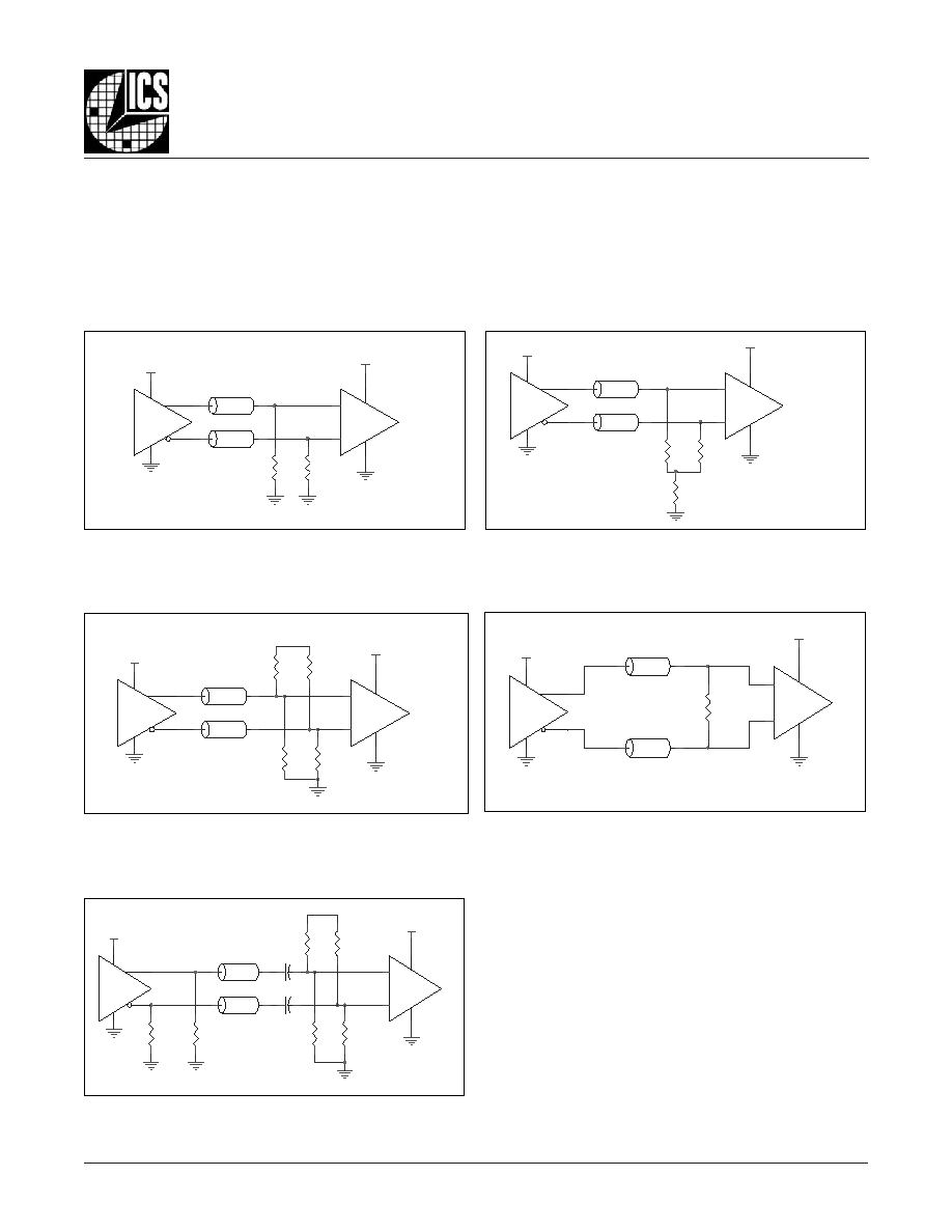
IGURE
3C. H
I
P
ER
C
LOCK
S CLK/
N
CLK I
NPUT
D
RIVEN
BY
3.3V LVPECL D
RIVER
F
IGURE
3B. H
I
P
ER
C
LOCK
S CLK/
N
CLK I
NPUT
D
RIVEN
BY
3.3V LVPECL D
RIVER
F
IGURE
3D. H
I
P
ER
C
LOCK
S CLK/
N
CLK I
NPUT
D
RIVEN
BY
3.3V LVDS D
RIVER
3.3V
R1
50
R3
50
Zo = 50 Ohm
LVPECL
Zo = 50 Ohm
HiPerClockS
CLK
nCLK
3.3V
Input
R2
50
Zo = 50 Ohm
Input
HiPerClockS
CLK
nCLK
3.3V
R3
125
R2
84
Zo = 50 Ohm
3.3V
R4
125
LVPECL
R1
84
3.3V
D
IFFERENTIAL
C
LOCK
I
NPUT
I
NTERFACE
The CLK /nCLK accepts LVDS, LVPECL, HSTL, SSTL, HCSL
and other differential signals. Both V
SWING
and V
OH
must meet the
V
PP
and V
CMR
input requirements. Figures 3A to 3E show inter-
face examples for the HiPerClockS CLK/nCLK input driven by
the most common driver types. The input interfaces suggested
F
IGURE
3A. H
I
P
ER
C
LOCK
S CLK/
N
CLK I
NPUT
D
RIVEN
BY
ICS H
I
P
ER
C
LOCK
S HSTL D
RIVER
here are examples only. Please consult with the vendor of the
driver component to confirm the driver termination requirements.
For example in
Figure 4A, the input termination applies for ICS
HiPerClockS HSTL drivers. If you are using an LVHSTL driver
from another vendor, use their termination recommendation.
1.8V
R2
50
Input
LVHSTL Driver
ICS
HiPerClockS
R1
50
LVHSTL
3.3V
Zo = 50 Ohm
Zo = 50 Ohm
HiPerClockS
CLK
nCLK
F
IGURE
3E. H
I
P
ER
C
LOCK
S CLK/
N
CLK I
NPUT
D
RIVEN
BY
3.3V LVPECL D
RIVER
WITH
AC C
OUPLE
Zo = 50 Ohm
R3
125
HiPerClockS
CLK
nCLK
3.3V
R5
100 - 200
3.3V
R2
84
3.3V
R6
100 - 200
Input
R5,R6 locate near the driver pin.
Zo = 50 Ohm
R1
84
R4
125
C2
LVPECL
C1
Zo = 50 Ohm
R1
100
3.3V
LVDS_Driv er
Zo = 50 Ohm
Receiv er
CLK
nCLK
3.3V
8524AY
www.icst.com/products/hiperclocks.html
REV. B SEPTEMBER 18, 2003
10
Integrated
Circuit
Systems, Inc.
ICS8524
L
OW
S
KEW
, 1-
TO
-22
D
IFFERENTIAL
-
TO
-HSTL F
ANOUT
B
UFFER
LVPECL C
LOCK
I
NPUT
I
NTERFACE
The PCLK /nPCLK accepts LVPECL, CML, SSTL and other
differential signals. Both V
SWING
and V
OH
must meet the V
PP
and V
CMR
input requirements.
Figures 4A to 4E show inter-
face examples for the HiPerClockS PCLK/nPCLK input driven
by the most common driver types. The input interfaces sug-
gested here are examples only. If the driver is from another
vendor, use their termination recommendation. Please con-
sult with the vendor of the driver component to confirm the
driver termination requirements.
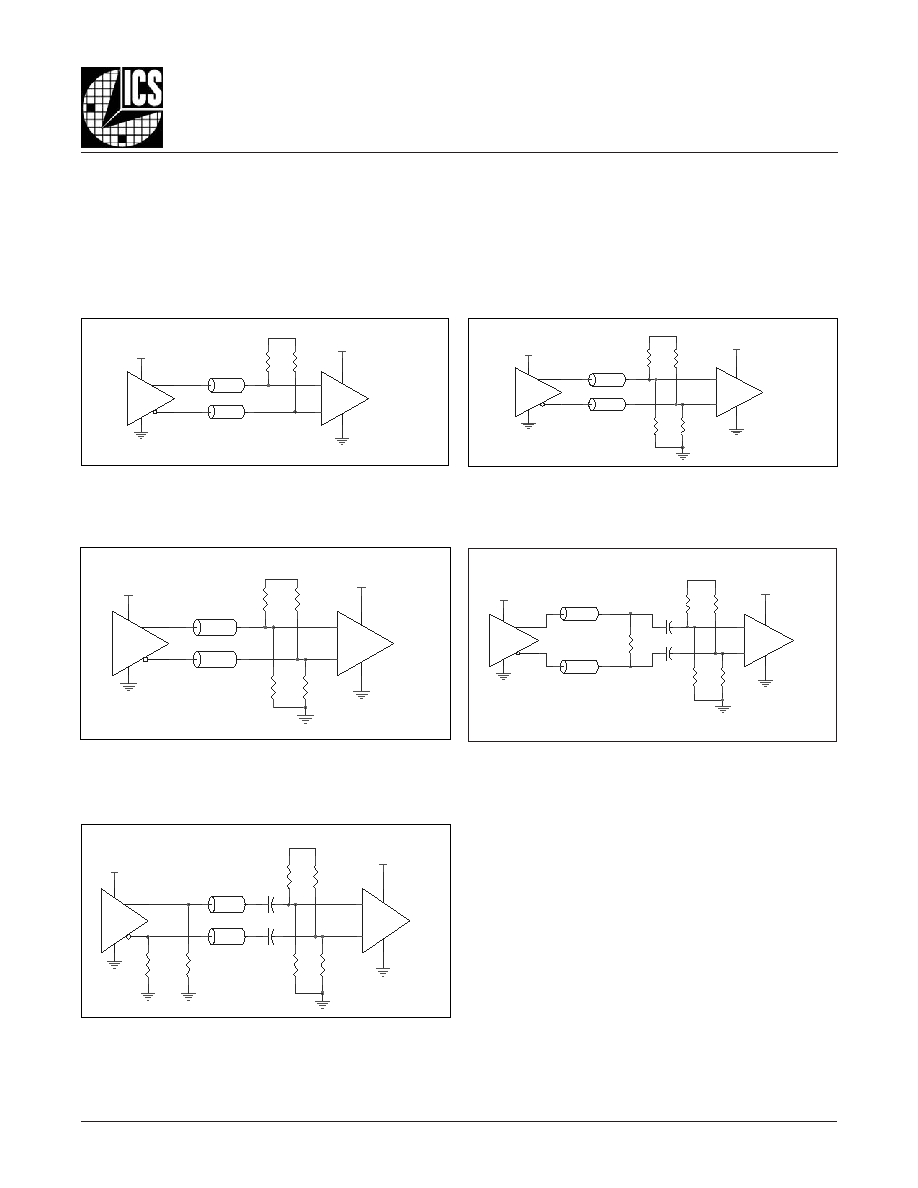
F
IGURE
4A. H
I
P
ER
C
LOCK
S PCLK/
N
PCLK I
NPUT
D
RIVEN
BY
A
CML D
RIVER
F
IGURE
4B. H
I
P
ER
C
LOCK
S PCLK/
N
PCLK I
NPUT
D
RIVEN
BY
AN
SSTL D
RIVER
F
IGURE
4C. H
I
P
ER
C
LOCK
S PCLK/
N
PCLK I
NPUT
D
RIVEN
BY
A
3.3V LVPECL D
RIVER
F
IGURE
4D. H
I
P
ER
C
LOCK
S PCLK/
N
PCLK I
NPUT
D
RIVEN
BY
A
3.3V LVDS D
RIVER
HiPerClockS
PCLK
nPCLK
PCLK/nPCLK
3.3V
R2
50
R1
50
3.3V
Zo = 50 Ohm
CML
3.3V
Zo = 50 Ohm
PCLK/nPCLK
2.5V
Zo = 60 Ohm
SSTL
HiPerClockS
PCLK
nPCLK
R2
120
3.3V
R3
120
Zo = 60 Ohm
R1
120
R4
120
2.5V
Zo = 50 Ohm
Input
HiPerClockS
CLK
nCLK
3.3V
R3
125
R2
84
Zo = 50 Ohm
3.3V
R4
125
LVPECL
R1
84
3.3V
F
IGURE
4E. H
I
P
ER
C
LOCK
S PCLK/
N
PCLK I
NPUT
D
RIVEN
BY
A
3.3V LVPECL D
RIVER
WITH
AC C
OUPLE
3.3V
R5
100 - 200
3.3V
3.3V
HiPerClockS
PCLK
nPCLK
R1
125
PCLK/nPCLK
R2
125
R3
84
C1
C2
Zo = 50 Ohm
R4
84
Zo = 50 Ohm
R6
100 - 200
3.3V LVPECL
C2
R2
1K
R5
100
Zo = 50 Ohm
3.3V
3.3V
C1
R3
1K
LVDS
R4
1K
HiPerClockS
PCLK
nPCLK
R1
1K
Zo = 50 Ohm
3.3V
PC L K /n PC LK
8524AY
www.icst.com/products/hiperclocks.html
REV. B SEPTEMBER 18, 2003
11
Integrated
Circuit
Systems, Inc.
ICS8524
L
OW
S
KEW
, 1-
TO
-22
D
IFFERENTIAL
-
TO
-HSTL F
ANOUT
B
UFFER
VDDO=1.8V
C7
0.1uF
(U1-48)
(U1-64)
+
-
R12
1K
Zo = 50
C2
0.1uF
R2
50
(U1-32)
C3
0.1uF
(U1-33)
C1
0.1uF
R1
50
Zo = 50
C5
0.1uF
C6
0.1uF
(U1-1)
C4
0.1uF
(U1-49)
VDD=3.3V
R10
50
Zo = 50
LVHSTL Driv er
R8
50
(U1-17)
Zo = 50
R9
50
C8
0.1uF
1.8V
VDDO=1.8V
+
-
VDD=3.3V
Zo = 50 Ohm
(U1-16)
U3
ICS8524
1
2
3
4
5
6
7
8
9
10
11
12
13
14
15
16
17
18
19
20
21
22
23
24
25
26
39
38
37
36
35
34
33
32
31
30
29
28
27
52
51
50
49
48
47
46
45
44
43
42
41
40
53
58
57
56
55
54
62
61
60
59
64
63
VDDO
nc
nc
VDD
CLK
nCLK
CLK_SEL
PCLK
nPCLK
GND
OE
nc
nc
nQ21
Q21
VDDO
VD
D
O
nQ
2
0
Q2
0
nQ
1
9
Q1
9
nQ
1
8
Q1
8
nQ
1
7
Q1
7
nQ
1
6
Q11
nQ11
Q12
nQ12
Q13
nQ13
VDDO
VD
D
O
Q1
4
nQ
1
4
Q1
5
nQ
1
5
Q1
6
nQ
5
Q6
nQ
6
V
DDO
VDDO
Q7
nQ7
Q8
nQ8
Q9
nQ9
Q10
nQ10
Q5
nQ
2
Q3
nQ
3
Q4
nQ
4
nQ
0
Q1
nQ
1
Q2
V
DDO
Q0
C9
0.1u
R11
1K
R7
50
Zo = 50 Ohm
S
CHEMATIC
E
XAMPLE
Figure 5 shows a schematic example of the ICS8524. In this
example, the input is driven by an ICS HiPerClockS HSTL driver.
The decoupling capacitors should be physically located near the
F
IGURE
5. ICS8524 HSTL B
UFFER
S
CHEMATIC
E
XAMPLE
power pin. For ICS8524, the unused clock outputs can be left
floating.
EXPOSED PAD
Expose Metal Pad
(GROUND PAD)
GROUND PLANE
SOLDER
SIGNAL
TRACE
SIGNAL
TRACE
THERM AL VIA
SOLDER M ASK
F
IGURE
6. P.C. B
OARD
FOR
E
XPOSED
P
AD
T
HERMAL
R
ELEASE
P
ATH
E
XAMPLE
T
HERMAL
R
ELEASE
P
ATH
The expose metal pad provides heat transfer from the device to
the P.C. board. The expose metal pad is ground pad connected
to ground plane through thermal via. The exposed pad on the
device to the exposed metal pad on the PCB is contacted through
solder as shown in
Figure 6. For further information, please re-
fer to the Application Note on Surface Mount Assembly of
Amkor's Thermally /Electrically Enhance Leadframe Base Pack-
age, Amkor Technology.

8524AY
www.icst.com/products/hiperclocks.html
REV. B SEPTEMBER 18, 2003
12
Integrated
Circuit
Systems, Inc.
ICS8524
L
OW
S
KEW
, 1-
TO
-22
D
IFFERENTIAL
-
TO
-HSTL F
ANOUT
B
UFFER
P
OWER
C
ONSIDERATIONS
This section provides information on power dissipation and junction temperature for the ICS8524.
Equations and example calculations are also provided.
1. Power Dissipation.
The total power dissipation for the ICS8524 is the sum of the core power plus the power dissipated in the load(s).
The following is the power dissipation for V
DD
= 3.3V + 5% = 3.465V, which gives worst case results.
NOTE: Please refer to Section 3 for details on calculating power dissipated in the load.
�
Power (core)
MAX
= V
DD_MAX
* I
DD_MAX
= 3.465V * 220mA = 762.3mW
�
Power (outputs)
MAX
= 32.8mW/Loaded Output pair
If all outputs are loaded, the total power is 22 * 32.8mW = 721.6mW
Total Power
_MAX
(3.465V, with all outputs switching) = 762.3mW + 721.6mW = 1483.9mW
2. Junction Temperature.
Junction temperature, Tj, is the temperature at the junction of the bond wire and bond pad and directly affects the reliability of the
device. The maximum recommended junction temperature for HiPerClockS
TM
devices is 125�C.
The equation for Tj is as follows: Tj =
JA
* Pd_total + T
A
Tj = Junction Temperature
JA
= Junction-to-Ambient Thermal Resistance
Pd_total = Total Device Power Dissipation (example calculation is in section 1 above)
T
A
= Ambient Temperature
In order to calculate junction temperature, the appropriate junction-to-ambient thermal resistance
JA
must be used. Assuming an
air flow of 500 linear feet per minute and a multi-layer board, the appropriate value is 15.1�C/W per Table 6 below.
Therefore, Tj for an ambient temperature of 85�C with all outputs switching is:
85�C + 1.484W * 15.1�C/W = 107.4�C. This is well below the limit of 125�C.
This calculation is only an example. Tj will obviously vary depending on the number of loaded outputs, supply voltage, air flow,
and the type of board (single layer or multi-layer).
JA
by Velocity (Linear Feet per Minute)
0
200
500
Multi-Layer PCB, JEDEC Standard Test Boards
22.3�C/W
17.2�C/W
15.1�C/W
NOTE: Most modern PCB designs use multi-layered boards. The data in the second row pertains to most designs.
T
ABLE
6. T
HERMAL
R
ESISTANCE
JA
FOR
64-
PIN
TQFP, E-P
AD
F
ORCED
C
ONVECTION

8524AY
www.icst.com/products/hiperclocks.html
REV. B SEPTEMBER 18, 2003
13
Integrated
Circuit
Systems, Inc.
ICS8524
L
OW
S
KEW
, 1-
TO
-22
D
IFFERENTIAL
-
TO
-HSTL F
ANOUT
B
UFFER
3. Calculations and Equations.
The purpose of this section is to derive the power dissipated into the load.
HSTL output driver circuit and termination are shown in
Figure 7.
T
o calculate worst case power dissipation into the load, use the following equations which assume a 50
load.
Pd_H is power dissipation when the output drives high.
Pd_L is the power dissipation when the output drives low.
Pd_H = (V
OH_MIN
/R
L
) * (V
DDO_MAX
- V
OH_MIN
)
Pd_L = (V
OL_MAX
/R
L
) * (V
DDO_MAX
- V
OL_MAX
)
Pd_H = (1V/50
) * (2V - 1V) = 20mW
Pd_L = (0.4V/50
) * (2V - 0.4V) = 12.8mW
Total Power Dissipation per output pair = Pd_H + Pd_L = 32.8mW
F
IGURE
7. HSTL D
RIVER
C
IRCUIT
AND
T
ERMINATION
V
DDO
V
OUT
RL
50
Q1

8524AY
www.icst.com/products/hiperclocks.html
REV. B SEPTEMBER 18, 2003
14
Integrated
Circuit
Systems, Inc.
ICS8524
L
OW
S
KEW
, 1-
TO
-22
D
IFFERENTIAL
-
TO
-HSTL F
ANOUT
B
UFFER
R
ELIABILITY
I
NFORMATION
T
RANSISTOR
C
OUNT
The transistor count for ICS8524 is: 1474
T
ABLE
7.
JA
VS
. A
IR
F
LOW
T
ABLE
FOR
64 L
EAD
TQFP, E-P
AD
JA
by Velocity (Linear Feet per Minute)
0
200
500
Multi-Layer PCB, JEDEC Standard Test Boards
22.3�C/W
17.2�C/W
15.1�C/W
NOTE: Most modern PCB designs use multi-layered boards. The data in the second row pertains to most designs.
8524AY
www.icst.com/products/hiperclocks.html
REV. B SEPTEMBER 18, 2003
15
Integrated
Circuit
Systems, Inc.
ICS8524
L
OW
S
KEW
, 1-
TO
-22
D
IFFERENTIAL
-
TO
-HSTL F
ANOUT
B
UFFER
E2
D2
EXPOSED PAD
P
ACKAGE
O
UTLINE
- Y S
UFFIX
FOR
64 L
EAD
TQFP, E-P
AD
T
ABLE
8. P
ACKAGE
D
IMENSIONS
Reference Document: JEDEC Publication 95, MS-026
N
O
I
T
A
I
R
A
V
C
E
D
E
J
S
R
E
T
E
M
I
L
L
I
M
N
I
S
N
O
I
S
N
E
M
I
D
L
L
A
L
O
B
M
Y
S
D
C
B
M
U
M
I
N
I
M
L
A
N
I
M
O
N
M
U
M
I
X
A
M
N
4
6
A
-
-
-
-
0
2
.
1
1
A
5
0
.
0
-
-
5
1
.
0
2
A
5
9
.
0
.
1
5
0
.
1
b
7
1
.
0
2
2
.
0
7
2
.
0
c
9
0
.
0
-
-
0
2
.
0
D
C
I
S
A
B
0
0
.
2
1
1
D
C
I
S
A
B
0
0
.
0
1
2
D
.
f
e
R
0
0
.
5
E
C
I
S
A
B
0
0
.
2
1
1
E
C
I
S
A
B
0
0
.
0
1
2
E
.
f
e
R
0
0
.
5
e
C
I
S
A
B
0
5
.
0
L
5
4
.
0
0
6
.
0
5
7
.
0
0
�
-
-
7
�
c
c
c
-
-
-
-
8
0
.
0

8524AY
www.icst.com/products/hiperclocks.html
REV. B SEPTEMBER 18, 2003
16
Integrated
Circuit
Systems, Inc.
ICS8524
L
OW
S
KEW
, 1-
TO
-22
D
IFFERENTIAL
-
TO
-HSTL F
ANOUT
B
UFFER
T
ABLE
9. O
RDERING
I
NFORMATION
While the information presented herein has been checked for both accuracy and reliability, Integrated Circuit Systems, Incorporated (ICS) assumes no responsibility for either its use
or for infringement of any patents or other rights of third parties, which would result from its use. No other circuits, patents, or licenses are implied. This product is intended for use
in normal commercial applications. Any other applications such as those requiring extended temperature range, high reliability, or other extraordinary environmental requirements are
not recommended without additional processing by ICS. ICS reserves the right to change any circuitry or specifications without notice. ICS does not authorize or warrant any ICS
product for use in life support devices or critical medical instruments.
r
e
b
m
u
N
r
e
d
r
O
/
t
r
a
P
g
n
i
k
r
a
M
e
g
a
k
c
a
P
t
n
u
o
C
e
r
u
t
a
r
e
p
m
e
T
Y
A
4
2
5
8
S
C
I
Y
A
4
2
5
8
S
C
I
d
a
P
-
E
,
P
F
Q
T
d
a
e
l
4
6
y
a
r
t
r
e
p
0
6
1
C
�
5
8
o
t
C
�
0
T
Y
A
4
2
5
8
S
C
I
Y
A
4
2
5
8
S
C
I
l
e
e
R
d
n
a
e
p
a
T
n
o
d
a
P
-
E
,
P
F
Q
T
d
a
e
l
4
6
0
0
5
C
�
5
8
o
t
C
�
0

8524AY
www.icst.com/products/hiperclocks.html
REV. B SEPTEMBER 18, 2003
17
Integrated
Circuit
Systems, Inc.
ICS8524
L
OW
S
KEW
, 1-
TO
-22
D
IFFERENTIAL
-
TO
-HSTL F
ANOUT
B
UFFER
T
E
E
H
S
Y
R
O
T
S
I
H
N
O
I
S
I
V
E
R
v
e
R
e
l
b
a
T
e
g
a
P
e
g
n
a
h
C
f
o
n
o
i
t
p
i
r
c
s
e
D
e
t
a
D
B
5
T
1
5
6
.
n
o
i
t
c
e
s
s
e
r
u
t
a
e
F
o
t
r
e
t
t
i
J
e
s
a
h
P
d
e
d
d
A
.
w
o
r
r
e
t
t
i
J
e
s
a
h
P
d
e
d
d
a
-
e
l
b
a
T
s
c
i
t
s
i
r
e
t
c
a
r
a
h
C
C
A
.
n
o
i
t
c
e
s
r
e
t
t
i
J
e
s
a
h
P
e
v
i
t
i
d
d
A
d
e
d
d
A
3
0
/
8
1
/
9