Äîêóìåíòàöèÿ è îïèñàíèÿ www.docs.chipfind.ru
853001AG
www.icst.com/products/hiperclocks.html
REV. A JANUARY 29, 2005
1
Integrated
Circuit
Systems, Inc.
ICS853001
1:1, D
IFFERENTIAL
LVPECL-
TO
-
2.5V, 3.3V, 5V LVPECL/ECL B
UFFER
G
ENERAL
D
ESCRIPTION
The ICS853001 is a 1:1 Differential LVPECL-
to-LVPE C L B u f fe r a n d a m e m b e r o f t h e
HiPerClock S TM
family of High Perfor mance
Clock Solutions from ICS. The ICS853 001
may be used to regenerate LVPECL clocks which
may have been attenuated, across a long trace, or may also
be used as a differential-to-LVPECL translator. The differen-
tial input can accept the following differential input types:
LVPECL, LVDS and CML. The device also has an output en-
able pin for debug/test purposes. When the output is disabled,
it drives differential LOW (Q = LOW, nQ = HIGH). The
ICS853001 is packaged in either a 3mm x 3mm 8-pin TSSOP
or 3.9mm x 4.9mm 8-pin SOIC, making it ideal for use on
space-constrained boards.
F
EATURES
· 1:1 Differential LVPECL-to-LVPECL / ECL buffer
· 1 LVPECL clock output pair
· 1 Differential LVPECL PCLK, nPCLK input pair
· PCLK, nPCLK pair can accept the following
differential input levels: LVPECL, LVDS, CML
· Maximum output frequency: >2.5GHz
· Part-to-part skew: 100ps (maximum)
· Propagation delay: 500ps (maximum)
· Additive phase jitter, RMS: 0.03ps (typical)
· LVPECL mode operating voltage supply range:
V
CC
= 2.375V to 5.25V, V
EE
= 0V
· ECL mode operating voltage supply range:
V
CC
= 0V, V
EE
= -5.25V to -2.375V
· -40°C to 85°C ambient operating temperature
· Lead-Free package RoHS compliant
B
LOCK
D
IAGRAM
P
IN
A
SSIGNMENT
ICS853001
8-Lead TSSOP, 118 mil
3mm x 3mm x 0.95mm package body
G Package
Top View
V
CC
Q
nQ
V
EE
1
2
3
4
HiPerClockSTM
ICS
OE
PCLK
nPCLK
V
BB
8
7
6
5
Q
nQ
OE
PCLK
nPCLK
V
BB
D Q
LE
ICS853001
8-Lead SOIC
3.90mm x 4.90mm x 1.37mm package body
M Package
Top View
853001AG
www.icst.com/products/hiperclocks.html
REV. A JANUARY 29, 2005
2
Integrated
Circuit
Systems, Inc.
ICS853001
1:1, D
IFFERENTIAL
LVPECL-
TO
-
2.5V, 3.3V, 5V LVPECL/ECL B
UFFER
T
ABLE
1. P
IN
D
ESCRIPTIONS
T
ABLE
2. P
IN
C
HARACTERISTICS
r
e
b
m
u
N
e
m
a
N
e
p
y
T
n
o
i
t
p
i
r
c
s
e
D
1
V
C
C
r
e
w
o
P
.
n
i
p
y
l
p
p
u
s
e
v
i
t
i
s
o
P
3
,
2
Q
n
,
Q
t
u
p
t
u
O
.
s
l
e
v
e
l
e
c
a
f
r
e
t
n
i
L
C
E
P
V
L
.
r
i
a
p
t
u
p
t
u
o
l
a
i
t
n
e
r
e
f
f
i
D
4
V
E
E
r
e
w
o
P
.
n
i
p
y
l
p
p
u
s
e
v
i
t
a
g
e
N
5
V
B
B
t
u
p
t
u
O
V
t
a
e
g
a
t
l
o
v
s
a
i
b
l
a
n
i
m
o
N
C
C
.
V
8
3
.
1
-
6
K
L
C
P
n
t
u
p
n
I
/
p
u
ll
u
P
n
w
o
d
ll
u
P
V
.
t
u
p
n
i
k
c
o
l
c
L
C
E
P
V
L
l
a
i
t
n
e
r
e
f
f
i
d
g
n
i
t
r
e
v
n
I
C
C
t
f
e
l
n
e
h
w
t
l
u
a
f
e
d
2
/
.
s
l
e
v
e
l
e
c
a
f
r
e
t
n
i
L
M
C
,
S
D
V
L
,
L
C
E
P
V
L
t
p
e
c
c
a
n
a
C
.
g
n
i
t
a
o
l
f
7
K
L
C
P
t
u
p
n
I
n
w
o
d
ll
u
P
.
t
u
p
n
i
k
c
o
l
c
L
C
E
P
V
L
l
a
i
t
n
e
r
e
f
f
i
d
g
n
i
t
r
e
v
n
i
-
n
o
N
.
s
l
e
v
e
l
e
c
a
f
r
e
t
n
i
L
M
C
,
S
D
V
L
,
L
C
E
P
V
L
t
p
e
c
c
a
n
a
C
8
E
O
t
u
p
n
I
p
u
ll
u
P
d
e
l
b
a
n
e
s
i
t
u
p
t
u
o
e
h
t
,
H
G
I
H
c
i
g
o
l
n
e
h
W
.
e
l
b
a
n
e
t
u
p
t
u
o
H
G
I
H
e
v
i
t
c
A
c
i
g
o
l
s
e
v
i
r
d
t
u
p
t
u
o
e
h
t
,
W
O
L
c
i
g
o
l
n
e
h
W
.
k
c
o
l
c
t
u
p
n
i
e
h
t
s
w
o
ll
o
f
d
n
a
.
s
l
e
v
e
l
e
c
a
f
r
e
t
n
i
L
T
T
V
L
/
S
O
M
C
V
L
.
)
H
G
I
H
=
Q
n
,
W
O
L
=
Q
(
w
o
l
:
E
T
O
N
n
w
o
d
ll
u
P
d
n
a
p
u
ll
u
P
.
s
e
u
l
a
v
l
a
c
i
p
y
t
r
o
f
,
s
c
i
t
s
i
r
e
t
c
a
r
a
h
C
n
i
P
,
2
e
l
b
a
T
e
e
S
.
s
r
o
t
s
i
s
e
r
t
u
p
n
i
l
a
n
r
e
t
n
i
o
t
r
e
f
e
r
l
o
b
m
y
S
r
e
t
e
m
a
r
a
P
s
n
o
i
t
i
d
n
o
C
t
s
e
T
m
u
m
i
n
i
M
l
a
c
i
p
y
T
m
u
m
i
x
a
M
s
t
i
n
U
R
N
W
O
D
L
L
U
P
r
o
t
s
i
s
e
R
n
w
o
d
ll
u
P
t
u
p
n
I
5
.
7
3
K
R
P
U
L
L
U
P
r
o
t
s
i
s
e
R
p
u
ll
u
P
t
u
p
n
I
5
.
7
3
K
853001AG
www.icst.com/products/hiperclocks.html
REV. A JANUARY 29, 2005
3
Integrated
Circuit
Systems, Inc.
ICS853001
1:1, D
IFFERENTIAL
LVPECL-
TO
-
2.5V, 3.3V, 5V LVPECL/ECL B
UFFER
T
ABLE
3A. P
OWER
S
UPPLY
DC C
HARACTERISTICS
,
V
CC
= 2.375V
TO
5.25V; V
EE
= 0V, T
A
= -40°C
TO
85°C
l
o
b
m
y
S
r
e
t
e
m
a
r
a
P
s
n
o
i
t
i
d
n
o
C
t
s
e
T
m
u
m
i
n
i
M
l
a
c
i
p
y
T
m
u
m
i
x
a
M
s
t
i
n
U
V
C
C
e
g
a
t
l
o
V
y
l
p
p
u
S
e
v
i
t
i
s
o
P
5
7
3
.
2
3
.
3
5
2
.
5
V
I
E
E
t
n
e
r
r
u
C
y
l
p
p
u
S
r
e
w
o
P
7
2
A
m
A
BSOLUTE
M
AXIMUM
R
ATINGS
NOTE: Stresses beyond those listed under Absolute
Maximum Ratings may cause permanent damage
to the device. These ratings are stress specifi-
cations only. Functional operation of product at
these conditions or any conditions beyond those
listed in the
DC Characteristics or AC Character-
istics is not implied. Exposure to absolute maxi-
mum rating conditions for extended periods may
affect product reliability.
Supply Voltage, V
CC
6V (LVPECL mode, V
EE
= 0)
Negative Supply Voltage, V
EE
-6V (ECL mode, V
CC
= 0)
Inputs, V
I
(LVPECL mode)
-0.5V to V
CC
+ 0.5 V
Inputs, V
I
(ECL mode)
0.5V to V
EE
- 0.5V
Outputs, I
O
Continuous Current
50mA
Surge Current
100mA
V
BB
Sink/Source, I
BB
± 0.5mA
Operating Temperature Range, TA -40°C to +85°C
Storage Temperature, T
STG
-65°C to 150°C
Package Thermal Impedance,
JA
8 Lead TSSOP
101.7°C/W (0 m/s)
8 Lead SOIC
112.7°C/W (0 lfpm)
(Junction-to-Ambient)
T
ABLE
3B. LVCMOS DC C
HARACTERISTICS
,
V
CC
= 2.375V
TO
5.25V; V
EE
= 0V, T
A
= -40°C
TO
85°C
l
o
b
m
y
S
r
e
t
e
m
a
r
a
P
s
n
o
i
t
i
d
n
o
C
t
s
e
T
m
u
m
i
n
i
M
l
a
c
i
p
y
T
m
u
m
i
x
a
M
s
t
i
n
U
V
H
I
e
g
a
t
l
o
V
h
g
i
H
t
u
p
n
I
E
O
V
7
.
0
C
C
V
C
C
3
.
0
+
V
V
L
I
e
g
a
t
l
o
V
w
o
L
t
u
p
n
I
E
O
3
.
0
-
V
3
.
0
C
C
V
I
H
I
t
n
e
r
r
u
C
h
g
i
H
t
u
p
n
I
E
O
V
C
C
V
=
N
I
0
5
1
A
µ
I
L
I
t
n
e
r
r
u
C
w
o
L
t
u
p
n
I
E
O
V
C
C
V
=
N
I
0
5
1
-
A
µ
T
ABLE
3C. LVCMOS DC C
HARACTERISTICS
,
V
CC
= 0V; V
EE
= -5.25V
TO
-2.375V, T
A
= -40°C
TO
85°C
l
o
b
m
y
S
r
e
t
e
m
a
r
a
P
s
n
o
i
t
i
d
n
o
C
t
s
e
T
m
u
m
i
n
i
M
l
a
c
i
p
y
T
m
u
m
i
x
a
M
s
t
i
n
U
V
H
I
e
g
a
t
l
o
V
h
g
i
H
t
u
p
n
I
E
O
V
3
.
0
E
E
3
.
0
V
V
L
I
e
g
a
t
l
o
V
w
o
L
t
u
p
n
I
E
O
V
E
E
3
.
0
-
V
7
.
0
E
E
V
I
H
I
t
n
e
r
r
u
C
h
g
i
H
t
u
p
n
I
E
O
V
C
C
V
=
N
I
0
5
1
A
µ
I
L
I
t
n
e
r
r
u
C
w
o
L
t
u
p
n
I
E
O
V
C
C
V
=
N
I
0
5
1
-
A
µ
853001AG
www.icst.com/products/hiperclocks.html
REV. A JANUARY 29, 2005
4
Integrated
Circuit
Systems, Inc.
ICS853001
1:1, D
IFFERENTIAL
LVPECL-
TO
-
2.5V, 3.3V, 5V LVPECL/ECL B
UFFER
T
ABLE
4. AC C
HARACTERISTICS
,
V
CC
= 0V; V
EE
= -5.25V
TO
-2.375V
OR
V
CC
= 2.375
TO
5.25V; V
EE
= 0V, T
A
= -40°C
TO
85°C
l
o
b
m
y
S
r
e
t
e
m
a
r
a
P
s
n
o
i
t
i
d
n
o
C
t
s
e
T
m
u
m
i
n
i
M
l
a
c
i
p
y
T
m
u
m
i
x
a
M
s
t
i
n
U
f
X
A
M
y
c
n
e
u
q
e
r
F
t
u
p
t
u
O
5
.
2
>
z
H
G
t
D
P
1
E
T
O
N
;
y
a
l
e
D
n
o
i
t
a
g
a
p
o
r
P
0
5
2
0
0
5
s
p
t
)
p
p
(
k
s
3
,
2
E
T
O
N
;
w
e
k
S
t
r
a
P
-
o
t
-
t
r
a
P
0
0
1
s
p
t t
i
j
;
S
M
R
,
r
e
t
t
i
J
e
s
a
h
P
e
v
i
t
i
d
d
A
r
e
f
f
u
B
n
o
i
t
c
e
S
r
e
t
t
i
J
e
s
a
h
P
e
v
i
t
i
d
d
A
o
t
r
e
f
e
r
:
e
g
n
a
R
n
o
i
t
a
r
g
e
t
n
I
,
z
H
M
2
5
.
5
5
1
z
H
M
0
2
-
z
H
K
2
1
3
0
.
0
s
p
t
R
t
/
F
e
m
i
T
ll
a
F
/
e
s
i
R
t
u
p
t
u
O
%
0
8
o
t
%
0
2
0
5
0
5
2
s
p
c
d
o
e
l
c
y
C
y
t
u
D
t
u
p
t
u
O
z
H
G
1
V
C
C
V
,
V
6
.
3
o
t
V
5
7
3
.
2
=
E
E
0
=
8
4
2
5
%
V
C
C
V
,
V
5
2
.
5
o
t
V
6
.
3
>
E
E
r
o
0
=
V
E
E
V
,
V
6
.
3
-
o
t
V
5
2
.
5
-
=
C
C
0
=
6
4
4
5
%
t
a
d
e
r
u
s
a
e
m
e
r
a
s
r
e
t
e
m
a
r
a
p
ll
A
.
d
e
t
o
n
e
s
i
w
r
e
h
t
o
s
s
e
l
n
u
,
z
H
G
7
.
1
.
t
n
i
o
p
g
n
i
s
s
o
r
c
t
u
p
t
u
o
l
a
i
t
n
e
r
e
f
f
i
d
e
h
t
o
t
t
n
i
o
p
g
n
i
s
s
o
r
c
t
u
p
n
i
l
a
i
t
n
e
r
e
f
f
i
d
e
h
t
m
o
r
f
d
e
r
u
s
a
e
M
:
1
E
T
O
N
d
n
a
s
e
g
a
t
l
o
v
y
l
p
p
u
s
e
m
a
s
e
h
t
t
a
g
n
i
t
a
r
e
p
o
s
e
c
i
v
e
d
t
n
e
r
e
f
f
i
d
n
o
s
t
u
p
t
u
o
n
e
e
w
t
e
b
w
e
k
s
s
a
d
e
n
i
f
e
D
:
2
E
T
O
N
d
e
r
u
s
a
e
m
e
r
a
s
t
u
p
t
u
o
e
h
t
,
e
c
i
v
e
d
h
c
a
e
n
o
s
t
u
p
n
i
f
o
e
p
y
t
e
m
a
s
e
h
t
g
n
i
s
U
.
s
n
o
i
t
i
d
n
o
c
d
a
o
l
l
a
u
q
e
h
t
i
w
.
s
t
n
i
o
p
s
s
o
r
c
l
a
i
t
n
e
r
e
f
f
i
d
e
h
t
t
a
.
5
6
d
r
a
d
n
a
t
S
C
E
D
E
J
h
t
i
w
e
c
n
a
d
r
o
c
c
a
n
i
d
e
n
i
f
e
d
s
i
r
e
t
e
m
a
r
a
p
s
i
h
T
:
3
E
T
O
N
T
ABLE
3D. LVPECL DC C
HARACTERISTICS
,
V
CC
= 2.375V
TO
5.25V; V
EE
= 0V, T
A
= -40°C
TO
85°C
l
o
b
m
y
S
r
e
t
e
m
a
r
a
P
s
n
o
i
t
i
d
n
o
C
t
s
e
T
m
u
m
i
n
i
M
l
a
c
i
p
y
T
m
u
m
i
x
a
M
s
t
i
n
U
I
H
I
t
n
e
r
r
u
C
h
g
i
H
t
u
p
n
I
K
L
C
P
V
C
C
V
=
N
I
0
0
2
A
µ
K
L
C
P
n
V
C
C
V
=
N
I
0
0
2
A
µ
I
L
I
t
n
e
r
r
u
C
w
o
L
t
u
p
n
I
K
L
C
P
V
C
C
V
,
5
2
.
5
=
N
I
V
0
=
0
0
2
-
A
µ
K
L
C
P
n
V
C
C
V
,
V
5
2
.
5
=
N
I
V
0
=
0
0
2
-
A
µ
V
P
P
e
g
a
t
l
o
V
t
u
p
n
I
k
a
e
P
-
o
t
-
k
a
e
P
5
1
.
0
2
.
1
V
V
R
M
C
2
,
1
E
T
O
N
;
e
g
a
t
l
o
V
t
u
p
n
I
e
d
o
M
n
o
m
m
o
C
2
.
1
V
C
C
V
V
H
O
3
E
T
O
N
;
e
g
a
t
l
o
V
h
g
i
H
t
u
p
t
u
O
V
C
C
5
0
0
.
1
-
V
V
L
O
3
E
T
O
N
;
e
g
a
t
l
o
V
w
o
L
t
u
p
t
u
O
V
C
C
8
7
.
1
-
V
V
G
N
I
W
S
g
n
i
w
S
e
g
a
t
l
o
V
t
u
p
t
u
O
k
a
e
P
-
o
t
-
k
a
e
P
6
.
0
0
.
1
V
V
B
B
e
g
a
t
l
o
V
s
a
i
B
V
C
C
4
4
.
1
-
V
C
C
8
3
.
1
-
V
C
C
2
3
.
1
-
V
V
s
a
d
e
n
i
f
e
d
s
i
e
g
a
t
l
o
v
e
d
o
m
n
o
m
m
o
C
:
1
E
T
O
N
H
I
.
V
s
i
K
L
C
P
n
,
K
L
C
P
r
o
f
e
g
a
t
l
o
v
t
u
p
n
i
m
u
m
i
x
a
m
e
h
t
,
s
n
o
i
t
a
c
il
p
p
a
d
e
d
n
e
e
l
g
n
i
s
r
o
F
:
2
E
T
O
N
C
C
.
V
3
.
0
+
0
5
h
t
i
w
d
e
t
a
n
i
m
r
e
t
s
t
u
p
t
u
O
:
3
E
T
O
N
V
o
t
C
C
.
V
2
-
853001AG
www.icst.com/products/hiperclocks.html
REV. A JANUARY 29, 2005
5
Integrated
Circuit
Systems, Inc.
ICS853001
1:1, D
IFFERENTIAL
LVPECL-
TO
-
2.5V, 3.3V, 5V LVPECL/ECL B
UFFER
A
DDITIVE
P
HASE
J
ITTER
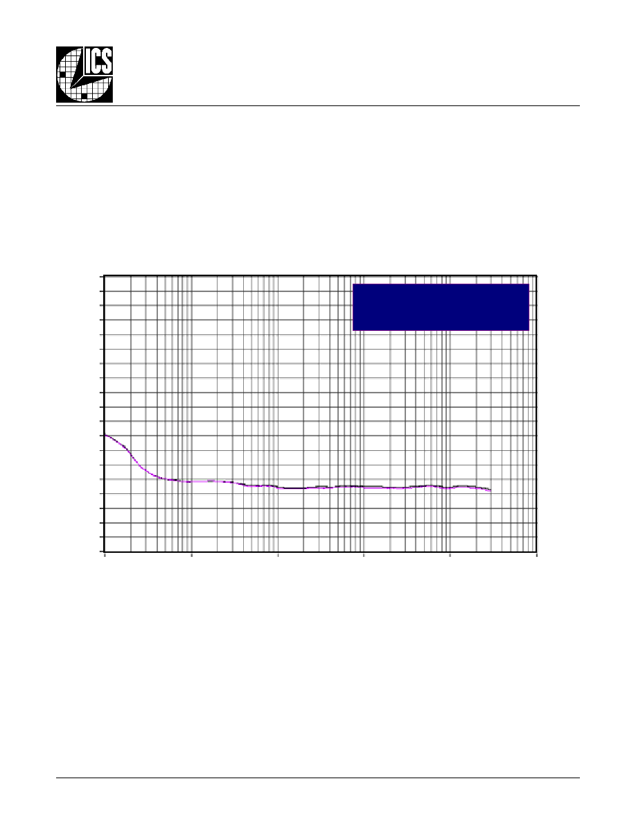
Additive Phase Jitter, RMS
@ 155.52MHz (12KHz to 20MHz)
= 0.03ps typical
0
-10
-20
-30
-40
-50
-60
-70
-80
-90
-100
-110
-120
-130
-140
-150
-160
-170
-180
-190
1k
10k
100k
1M
10M
100M
The spectral purity in a band at a specific offset from the funda-
mental compared to the power of the fundamental is called the
dBc Phase Noise. This value is normally expressed using a
Phase noise plot and is most often the specified plot in many
applications. Phase noise is defined as the ratio of the noise
power present in a 1Hz band at a specified offset from the fun-
damental frequency to the power value of the fundamental. This
ratio is expressed in decibels (dBm) or a ratio of the power in
As with most timing specifications, phase noise measurements
have issues. The primary issue relates to the limitations of the
equipment. Often the noise floor of the equipment is higher than
the noise floor of the device. This is illustrated above. The de-
the 1Hz band to the power in the fundamental. When the re-
quired offset is specified, the phase noise is called a
dBc value,
which simply means dBm at a specified offset from the funda-
mental. By investigating jitter in the frequency domain, we get a
better understanding of its effects on the desired application over
the entire time record of the signal. It is mathematically possible
to calculate an expected bit error rate given a phase noise plot.
vice meets the noise floor of what is shown, but can actually be
lower. The phase noise is dependant on the input source and
measurement equipment.
O
FFSET
F
ROM
C
ARRIER
F
REQUENCY
(H
Z
)
SSB P
HASE
N
OISE
dBc/H
Z
Document Outline
- General Description
- Features
- Block Diagram
- Pin Assignment
- Pin Descriptions
- Pin Characteristics
- Absolute Maximum Ratings
- Power Supply DC Characteristics
- LVCMOS DC Characteristics
- LVCMOS/ECL DC Characteristics
- LVPECL DC Characteristics
- AC Characteristics
- Parameter Measurement Information
- Output Load AC Test Circuit Diagram
- Differential Input Level Diagram
- Part-to-Part Skew Diagram
- Propagation Delay Diagram
- Output Rise/Fall Time Diagram
- Output Duty Cycle/Pulse Width/Period Diagram
- Application Information
- Wiring the Differential Input to Accept Single Ended LVCMOS Levels
- Wiring the Differential Input to Accept Single Ended LVPECL Level
- Termination for 2.5V LVPECL Output
- Termination for 3.3V LVPECL Output
- Termination for 5V LVPECL Output
- LVPECL Clock Input Interface
- Application Schematic Example
- Power Considerations
- Power Dissipation
- Junction Temperature
- Thermal Resistance for 8-Pin TSSOP
- Thermal Resistance for 8-Pin SOIC
- Calculations & Equations
- LVPECL Driver Circuit & Termination Diagram
- Reliability Information
- Transistor Count
- Package Outline for 8 Lead TSSOP
- Package Dimensions for 8 Lead TSSOP
- Package Outline for 8 Lead SOIC
- Package Dimensions for 8 Lead SOIC
- Ordering Information