Document Outline
- General Description
- Features
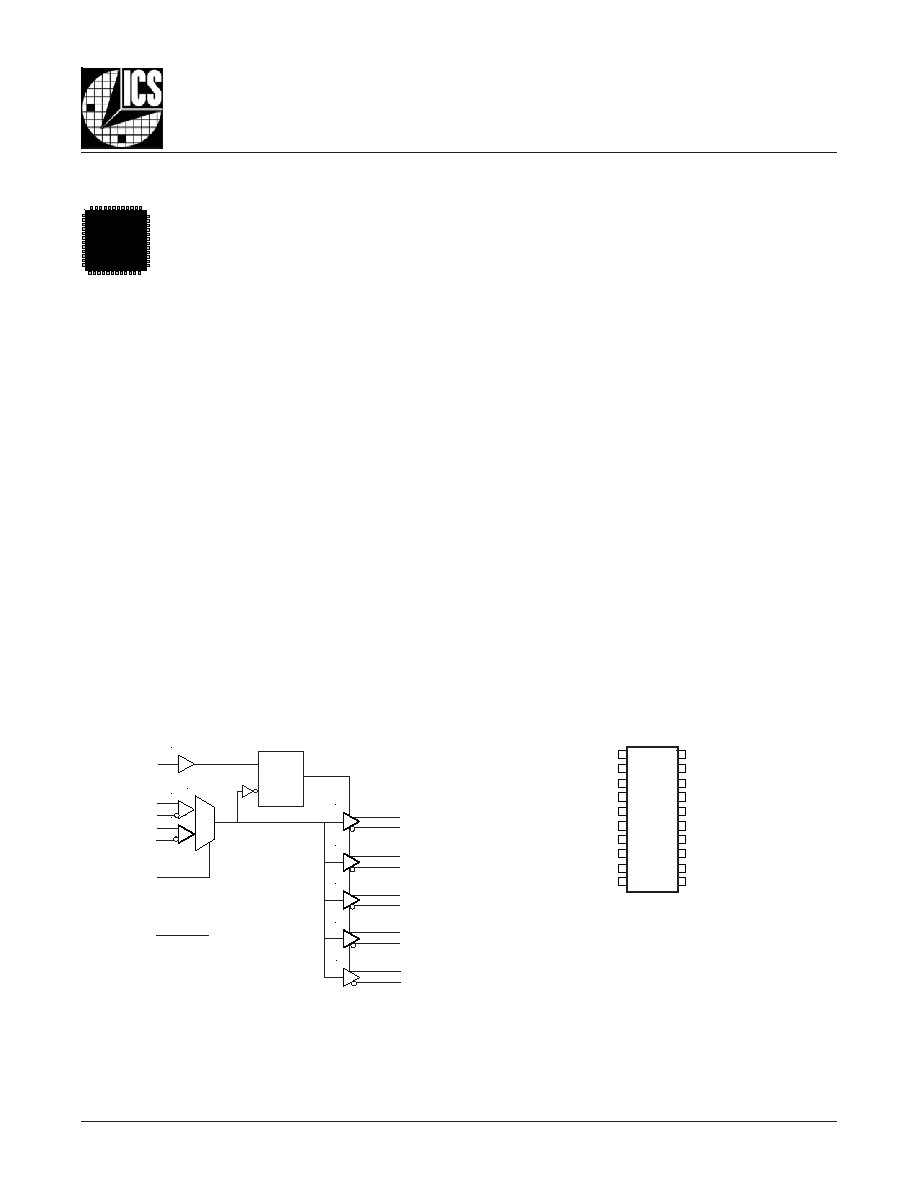
- Block Diagram
- Pin Assignment
- Pin Descriptions
- Pin Characteristics
- Control Input Function Table
- nEN Timing Diagram
- Clock Input Function Table
- Absolute Maximum Ratings
- Power Supply DC Characteristics
- LVPECL 3.3V DC Characteristics
- LVPECL 2.5V DC Characteristics
- ECL DC Characteristics
- AC Characteristics
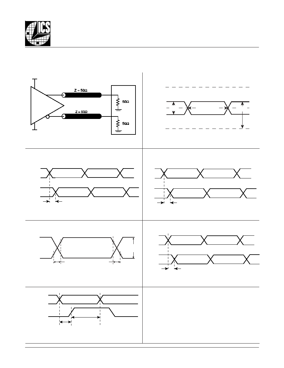
- Parameter Measurement Information
- Output Load AC Test Circuit Diagram
- Differential Input Level Diagram
- Part-to-Part Skew Diagram
- Output Skew Diagram
- Output Rise/Fall Time Diagram
- Propagation Delay Diagram
- Setup & Hold Time Diagram
- Application Information
- Wiring the Differential Input to Accept Single Ended Levels
- Termination for 3.3V LVPECL Outputs
- Termination for 2.5V LVPECL Outputs
- LVPECL Clock Input Interface
- HiPerClockS PCLK/nPCLK Input Driven by a CML Driver Diagram
- HiPerClockS PCLK/nPCLK Input Driven by an SSTL Driver Diagram
- HiPerClockS PCLK/nPCLK Input Driven by a 3.3V LVPECL Driver Diagram
- HiPerClockS PCLK/nPCLK Input Driven by a 3.3V LVDS Driver Diagram
- HiPerClockS PCLK/nPCLK Input Driven by a 3.3V LVPECL Driver w/AC Couple Diagram
- Schematic Example
- Power Considerations
- Power Dissipation
- Junction Temperature
- Thermal Resistance
- Calculations & Equations
- LVPECL Driver Circuit & Termination Diagram
- Reliability Information
- Transistor Count
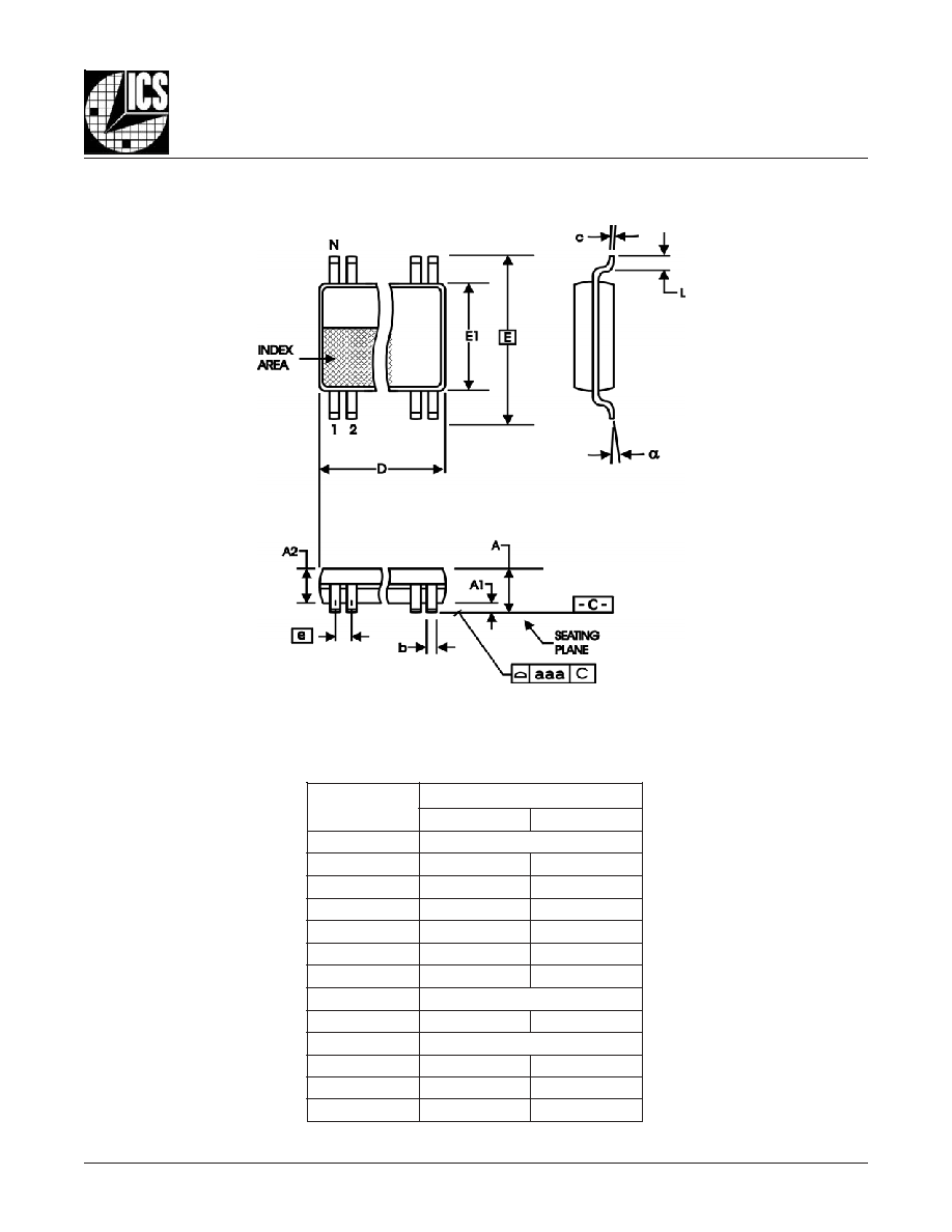
- Package Outline
- Package Dimensions
- Ordering Information
- Revision History Sheet
853014BG
www.icst.com/products/hiperclocks.html
REV. C MAY 13, 2005
1
Integrated
Circuit
Systems, Inc.
ICS853014
L
OW
S
KEW
, 1-
TO
-5
2.5V/3.3V D
IFFERENTIAL
-
TO
-LVPECL/ECL F
ANOUT
B
UFFER
G
ENERAL
D
ESCRIPTION
The ICS853014 is a low skew, high performance
1-to-5, 2.5V/3.3V Differential-to-LVPECL/ECL
Fanout Buffer and a member of the HiPerClockSTM
family of High Performance Clock Solutions
from ICS. The ICS853014 has two selectable
clock inputs.
Guaranteed output and par t-to-part skew characteristics
m a k e t h e I C S 8 5 3 0 1 4 i d e a l f o r t h o s e a p p l i c a t i o n s
demanding well defined performance and repeatability.
F
EATURES
� 5 differential LVPECL/ECL outputs
� 2 selectable differential LVPECL clock inputs
� PCLKx, nPCLKx pairs can accept the following
differential input levels: LVPECL, LVDS, CML, SSTL
� Maximum output frequency: > 2GHz
� Output skew: 13ps (typical)
� Part-to-part skew: 60ps (typical)
� Propagation delay: 460ps (typical)
� LVPECL mode operating voltage supply range:
V
CC
= 2.375V to 3.8V, V
EE
= 0V
� ECL mode operating voltage supply range:
V
CC
= 0V, V
EE
= -3.8V to -2.375V
� -40�C to 85�C ambient operating temperature
� Lead-Free package fully RoHS compliant
B
LOCK
D
IAGRAM
P
IN
A
SSIGNMENT
Q0
nQ0
Q1
nQ1
Q2
nQ2
Q3
nQ3
Q4
nQ4
1
2
3
4
5
6
7
8
9
10
20
19
18
17
16
15
14
13
12
11
V
CC
nEN
V
CC
nPCLK1
PCLK1
V
BB
nPCLK0
PCLK0
CLK_SEL
V
EE
HiPerClockSTM
ICS
ICS853014
20-Lead TSSOP
6.5mm x 4.4mm x 0.92mm package body
G Package
Top View
PCLK0
nPCLK0
PCLK1
nPCLK1
Q0
nQ0
Q1
nQ1
Q2
nQ2
Q3
nQ3
Q4
nQ4
0
1
nEN
CLK_SEL
D
Q
LE
0
1
V
BB

853014BG
www.icst.com/products/hiperclocks.html
REV. C MAY 13, 2005
2
Integrated
Circuit
Systems, Inc.
ICS853014
L
OW
S
KEW
, 1-
TO
-5
2.5V/3.3V D
IFFERENTIAL
-
TO
-LVPECL/ECL F
ANOUT
B
UFFER
T
ABLE
1. P
IN
D
ESCRIPTIONS
T
ABLE
2. P
IN
C
HARACTERISTICS
l
o
b
m
y
S
r
e
t
e
m
a
r
a
P
s
n
o
i
t
i
d
n
o
C
t
s
e
T
m
u
m
i
n
i
M
l
a
c
i
p
y
T
m
u
m
i
x
a
M
s
t
i
n
U
R
N
W
O
D
L
L
U
P
r
o
t
s
i
s
e
R
n
w
o
d
ll
u
P
t
u
p
n
I
5
7
k
R
2
/
C
C
V
s
r
o
t
s
i
s
e
R
n
w
o
d
ll
u
P
/
p
u
ll
u
P
0
5
k
r
e
b
m
u
N
e
m
a
N
e
p
y
T
n
o
i
t
p
i
r
c
s
e
D
2
,
1
0
Q
n
,
0
Q
t
u
p
t
u
O
.
s
l
e
v
e
l
e
c
a
f
r
e
t
n
i
L
C
E
/
L
C
E
P
V
L
.
r
i
a
p
t
u
p
t
u
o
l
a
i
t
n
e
r
e
f
f
i
D
4
,
3
1
Q
n
,
1
Q
t
u
p
t
u
O
.
s
l
e
v
e
l
e
c
a
f
r
e
t
n
i
L
C
E
/
L
C
E
P
V
L
.
r
i
a
p
t
u
p
t
u
o
l
a
i
t
n
e
r
e
f
f
i
D
6
,
5
2
Q
n
,
2
Q
t
u
p
t
u
O
.
s
l
e
v
e
l
e
c
a
f
r
e
t
n
i
L
C
E
/
L
C
E
P
V
L
.
r
i
a
p
t
u
p
t
u
o
l
a
i
t
n
e
r
e
f
f
i
D
8
,
7
3
Q
n
,
3
Q
t
u
p
t
u
O
.
s
l
e
v
e
l
e
c
a
f
r
e
t
n
i
L
C
E
/
L
C
E
P
V
L
.
r
i
a
p
t
u
p
t
u
o
l
a
i
t
n
e
r
e
f
f
i
D
0
1
,
9
4
Q
n
,
4
Q
t
u
p
t
u
O
.
s
l
e
v
e
l
e
c
a
f
r
e
t
n
i
L
C
E
/
L
C
E
P
V
L
.
r
i
a
p
t
u
p
t
u
o
l
a
i
t
n
e
r
e
f
f
i
D
1
1
V
E
E
r
e
w
o
P
.
n
i
p
y
l
p
p
u
s
e
v
i
t
a
g
e
N
2
1
L
E
S
_
K
L
C
t
u
p
n
I
n
w
o
d
ll
u
P
.
s
t
u
p
n
i
1
K
L
C
n
,
1
K
L
C
s
t
c
e
l
e
s
,
H
G
I
H
n
e
h
W
.
t
u
p
n
i
t
c
e
l
e
s
k
c
o
l
C
.
s
t
u
p
n
i
0
K
L
C
n
,
0
K
L
C
s
t
c
e
l
e
s
,
W
O
L
n
e
h
W
.
s
l
e
v
e
l
e
c
a
f
r
e
t
n
i
S
O
M
C
V
L
/
L
T
T
V
L
3
1
0
K
L
C
P
t
u
p
n
I
n
w
o
d
ll
u
P
.
t
u
p
n
i
k
c
o
l
c
L
C
E
P
V
L
l
a
i
t
n
e
r
e
f
f
i
d
g
n
i
t
r
e
v
n
i
-
n
o
N
4
1
0
K
L
C
P
n
t
u
p
n
I
V
.
t
u
p
n
i
k
c
o
l
c
L
C
E
P
V
L
l
a
i
t
n
e
r
e
f
f
i
d
g
n
i
t
r
e
v
n
I
C
C
.
g
n
i
t
a
o
l
f
t
f
e
l
n
e
h
w
t
l
u
a
f
e
d
2
/
5
1
V
B
B
t
u
p
t
u
O
.
e
g
a
t
l
o
v
s
a
i
B
6
1
1
K
L
C
P
t
u
p
n
I
n
w
o
d
ll
u
P
.
t
u
p
n
i
k
c
o
l
c
L
C
E
P
V
L
l
a
i
t
n
e
r
e
f
f
i
d
g
n
i
t
r
e
v
n
i
-
n
o
N
7
1
1
K
L
C
P
n
t
u
p
n
I
V
.
t
u
p
n
i
k
c
o
l
c
L
C
E
P
V
L
l
a
i
t
n
e
r
e
f
f
i
d
g
n
i
t
r
e
v
n
I
C
C
.
g
n
i
t
a
o
l
f
t
f
e
l
n
e
h
w
t
l
u
a
f
e
d
2
/
0
2
,
8
1
V
C
C
r
e
w
o
P
.
s
n
i
p
y
l
p
p
u
s
e
v
i
t
i
s
o
P
9
1
N
E
n
t
u
p
n
I
n
w
o
d
ll
u
P
.
t
u
p
n
i
k
c
o
l
c
w
o
ll
o
f
s
t
u
p
t
u
o
k
c
o
l
c
,
W
O
L
n
e
h
W
.
e
l
b
a
n
e
k
c
o
l
c
g
n
i
z
i
n
o
r
h
c
n
y
S
.
h
g
i
h
d
e
c
r
o
f
e
r
a
s
t
u
p
t
u
o
Q
n
,
w
o
l
d
e
c
r
o
f
e
r
a
s
t
u
p
t
u
o
Q
,
H
G
I
H
n
e
h
W
.
s
l
e
v
e
l
e
c
a
f
r
e
t
n
i
S
O
M
C
V
L
/
L
T
T
V
L
:
E
T
O
N
p
u
ll
u
P
d
n
a
n
w
o
d
ll
u
P
.
s
e
u
l
a
v
l
a
c
i
p
y
t
r
o
f
,
s
c
i
t
s
i
r
e
t
c
a
r
a
h
C
n
i
P
,
2
e
l
b
a
T
e
e
S
.
s
r
o
t
s
i
s
e
r
t
u
p
n
i
l
a
n
r
e
t
n
i
o
t
r
e
f
e
r
853014BG
www.icst.com/products/hiperclocks.html
REV. C MAY 13, 2005
3
Integrated
Circuit
Systems, Inc.
ICS853014
L
OW
S
KEW
, 1-
TO
-5
2.5V/3.3V D
IFFERENTIAL
-
TO
-LVPECL/ECL F
ANOUT
B
UFFER
T
ABLE
3A. C
ONTROL
I
NPUT
F
UNCTION
T
ABLE
T
ABLE
3B. C
LOCK
I
NPUT
F
UNCTION
T
ABLE
s
t
u
p
n
I
s
t
u
p
t
u
O
N
E
n
L
E
S
_
K
L
C
e
c
r
u
o
S
d
e
t
c
e
l
e
S
4
Q
:
0
Q
4
Q
n
:
0
Q
n
1
0
0
K
L
C
P
n
,
0
K
L
C
P
W
O
L
;
d
e
l
b
a
s
i
D
H
G
I
H
;
d
e
l
b
a
s
i
D
1
1
1
K
L
C
P
n
,
1
K
L
C
P
W
O
L
;
d
e
l
b
a
s
i
D
H
G
I
H
;
d
e
l
b
a
s
i
D
0
0
0
K
L
C
P
n
,
0
K
L
C
P
d
e
l
b
a
n
E
d
e
l
b
a
n
E
0
1
1
K
L
C
P
n
,
1
K
L
C
P
d
e
l
b
a
n
E
d
e
l
b
a
n
E
n
i
n
w
o
h
s
s
a
e
g
d
e
k
c
o
l
c
t
u
p
n
i
g
n
il
l
a
f
a
g
n
i
w
o
ll
o
f
d
e
l
b
a
n
e
r
o
d
e
l
b
a
s
i
d
e
r
a
s
t
u
p
t
u
o
k
c
o
l
c
e
h
t
,
s
e
h
c
t
i
w
s
N
E
n
r
e
t
f
A
r
u
g
i
F
e
.
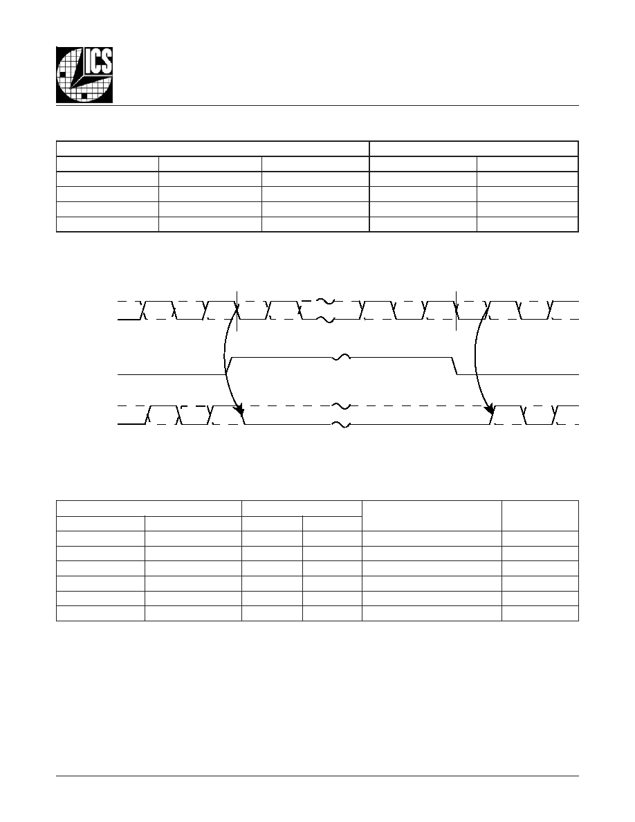
1
s
a
s
t
u
p
n
i
1
K
L
C
P
n
,
1
K
L
C
P
d
n
a
0
K
L
C
P
n
,
0
K
L
C
P
e
h
t
f
o
n
o
i
t
c
n
u
f
a
e
r
a
s
t
u
p
t
u
o
e
h
t
f
o
e
t
a
t
s
e
h
t
,
e
d
o
m
e
v
i
t
c
a
e
h
t
n
I
n
i
d
e
b
i
r
c
s
e
d
.
B
3
e
l
b
a
T
s
t
u
p
n
I
s
t
u
p
t
u
O
e
d
o
M
t
u
p
t
u
O
o
t
t
u
p
n
I
y
t
i
r
a
l
o
P
1
K
L
C
P
r
o
0
K
L
C
P
1
K
L
C
P
n
r
o
0
K
L
C
P
n
4
Q
:
0
Q
4
Q
n
:
0
Q
n
0
1
W
O
L
H
G
I
H
l
a
i
t
n
e
r
e
f
f
i
D
o
t
l
a
i
t
n
e
r
e
f
f
i
D
g
n
i
t
r
e
v
n
I
n
o
N
1
0
H
G
I
H
W
O
L
l
a
i
t
n
e
r
e
f
f
i
D
o
t
l
a
i
t
n
e
r
e
f
f
i
D
g
n
i
t
r
e
v
n
I
n
o
N
0
1
E
T
O
N
;
d
e
s
a
i
B
W
O
L
H
G
I
H
l
a
i
t
n
e
r
e
f
f
i
D
o
t
d
e
d
n
E
e
l
g
n
i
S
g
n
i
t
r
e
v
n
I
n
o
N
1
1
E
T
O
N
;
d
e
s
a
i
B
H
G
I
H
W
O
L
l
a
i
t
n
e
r
e
f
f
i
D
o
t
d
e
d
n
E
e
l
g
n
i
S
g
n
i
t
r
e
v
n
I
n
o
N
1
E
T
O
N
;
d
e
s
a
i
B
0
H
G
I
H
W
O
L
l
a
i
t
n
e
r
e
f
f
i
D
o
t
d
e
d
n
E
e
l
g
n
i
S
g
n
i
t
r
e
v
n
I
1
E
T
O
N
;
d
e
s
a
i
B
1
W
O
L
H
G
I
H
l
a
i
t
n
e
r
e
f
f
i
D
o
t
d
e
d
n
E
e
l
g
n
i
S
g
n
i
t
r
e
v
n
I
.
"
s
l
e
v
e
L
d
e
d
n
E
e
l
g
n
i
S
t
p
e
c
c
A
o
t
t
u
p
n
I
l
a
i
t
n
e
r
e
f
f
i
D
e
h
t
g
n
i
r
i
W
"
,
n
o
i
t
c
e
s
n
o
i
t
a
m
r
o
f
n
I
n
o
i
t
a
c
il
p
p
A
e
h
t
o
t
r
e
f
e
r
e
s
a
e
l
P
:
1
E
T
O
N
F
IGURE
1. nEN T
IMING
D
IAGRAM
Enabled
Disabled
nPCLK0, nPCLK1
PCLK0, PCLK1
nEN
nQ0:nQ4
Q0:Q4

853014BG
www.icst.com/products/hiperclocks.html
REV. C MAY 13, 2005
4
Integrated
Circuit
Systems, Inc.
ICS853014
L
OW
S
KEW
, 1-
TO
-5
2.5V/3.3V D
IFFERENTIAL
-
TO
-LVPECL/ECL F
ANOUT
B
UFFER
T
ABLE
4B. DC C
HARACTERISTICS
,
V
CC
= 3.3V, V
EE
= 0V
T
ABLE
4A. P
OWER
S
UPPLY
DC C
HARACTERISTICS
,
V
CC
= 2.375V
TO
3.8V; V
EE
= 0V
l
o
b
m
y
S
r
e
t
e
m
a
r
a
P
s
n
o
i
t
i
d
n
o
C
t
s
e
T
m
u
m
i
n
i
M
l
a
c
i
p
y
T
m
u
m
i
x
a
M
s
t
i
n
U
V
C
C
e
g
a
t
l
o
V
y
l
p
p
u
S
e
v
i
t
i
s
o
P
5
7
3
.
2
3
.
3
8
.
3
V
I
E
E
t
n
e
r
r
u
C
y
l
p
p
u
S
r
e
w
o
P
5
7
A
m
A
BSOLUTE
M
AXIMUM
R
ATINGS
NOTE: Stresses beyond those listed under Absolute
Maximum Ratings may cause permanent damage
to the device. These ratings are stress specifi-
cations only. Functional operation of product at
these conditions or any conditions beyond those
listed in the
DC Characteristics or AC Character-
istics is not implied. Exposure to absolute maxi-
mum rating conditions for extended periods may
affect product reliability.
Supply Voltage, V
CC
4.6V (LVPECL mode, V
EE
= 0)
Negative Supply Voltage, V
EE
-4.6V (ECL mode, V
CC
= 0)
Inputs, V
I
(LVPECL mode)
-0.5V to V
CC
+ 0.5V
Inputs, V
I
(ECL mode)
0.5V to V
EE
- 0.5V
Outputs, I
O
Continuous Current
50mA
Surge Current
100mA
V
BB
Sing/Source, I
BB
� 0.5mA
Operating Temperature Range, TA -40�C to +85�C
Storage Temperature, T
STG
-65�C to 150�C
Package Thermal Impedance,
JA
73.2�C/W (0 lfpm)
(Junction-to-Ambient)
l
o
b
m
y
S
r
e
t
e
m
a
r
a
P
C
�
0
4
-
C
�
5
2
C
�
5
8
s
t
i
n
U
n
i
M
p
y
T
x
a
M
n
i
M
p
y
T
x
a
M
n
i
M
p
y
T
x
a
M
V
H
O
1
E
T
O
N
;
e
g
a
t
l
o
V
h
g
i
H
t
u
p
t
u
O
5
7
1
.
2
5
7
2
.
2
8
3
.
2
5
2
2
.
2
5
9
2
.
2
5
7
3
.
2
2
2
.
2
5
9
2
.
2
5
6
3
.
2
V
V
L
O
1
E
T
O
N
;
e
g
a
t
l
o
V
w
o
L
t
u
p
t
u
O
5
0
4
.
1
5
4
5
.
1
8
6
.
1
5
2
4
.
1
2
5
.
1
5
1
6
.
1
4
4
.
1
5
3
5
.
1
3
6
.
1
V
V
H
I
e
g
a
t
l
o
V
h
g
i
H
t
u
p
n
I
)
d
e
d
n
E
-
e
l
g
n
i
S
(
5
7
0
.
2
6
3
.
2
5
7
0
.
2
6
3
.
2
5
7
0
.
2
6
3
.
2
V
V
L
I
e
g
a
t
l
o
V
w
o
L
t
u
p
n
I
)
d
e
d
n
E
-
e
l
g
n
i
S
(
3
4
.
1
5
6
7
.
1
3
4
.
1
5
6
7
.
1
3
4
.
1
5
6
7
.
1
V
V
B
B
2
E
T
O
N
;
e
c
n
e
r
e
f
e
R
e
g
a
t
l
o
V
t
u
p
t
u
O
6
8
.
1
8
9
.
1
6
8
.
1
8
9
.
1
6
8
.
1
8
9
.
1
V
V
R
M
C
e
g
a
t
l
o
V
h
g
i
H
t
u
p
n
I
4
,
3
E
T
O
N
;
e
g
n
a
R
e
d
o
M
n
o
m
m
o
C
2
.
1
3
.
3
2
.
1
3
.
3
2
.
1
3
.
3
V
I
H
I
t
u
p
n
I
t
n
e
r
r
u
C
h
g
i
H
3
D
,
2
D
,
1
D
,
0
D
3
D
n
,
2
D
n
,
1
D
n
,
0
D
n
0
5
1
0
5
1
0
5
1
A
�
I
L
I
t
u
p
n
I
t
n
e
r
r
u
C
w
o
L
3
D
,
2
D
,
1
D
,
0
D
0
1
-
0
1
-
0
1
-
A
�
3
D
n
,
2
D
n
,
1
D
n
,
0
D
n
0
5
1
-
0
5
1
-
0
5
1
-
A
�
V
h
t
i
w
1
:
1
y
r
a
v
s
r
e
t
e
m
a
r
a
p
t
u
p
t
u
o
d
n
a
t
u
p
n
I
C
C
V
.
E
E
.
V
5
.
0
-
o
t
V
5
2
9
.
0
+
y
r
a
v
n
a
c
0
5
h
t
i
w
d
e
t
a
n
i
m
r
e
t
s
t
u
p
t
u
O
:
1
E
T
O
N
V
o
t
C
C
.
V
2
-
V
.
d
e
t
i
m
il
s
i
n
o
i
t
a
r
e
p
o
t
u
p
n
i
d
e
d
n
e
-
e
l
g
n
i
S
:
2
E
T
O
N
C
C
.
e
d
o
m
L
C
E
P
V
L
n
i
V
3
V
s
a
d
e
n
i
f
e
d
s
i
e
g
a
t
l
o
v
e
d
o
m
n
o
m
m
o
C
:
3
E
T
O
N
H
I
.
1
K
L
C
P
n
,
1
K
L
C
P
d
n
a
0
K
C
L
P
n
,
0
K
L
C
P
r
o
f
e
g
a
t
l
o
v
t
u
p
n
i
m
u
m
i
x
a
m
e
h
t
,
s
n
o
i
t
a
c
il
p
p
a
d
e
d
n
e
-
e
l
g
n
i
s
r
o
F
:
4
E
T
O
N
V
s
i
C
C
.
V
3
.
0
+
853014BG
www.icst.com/products/hiperclocks.html
REV. C MAY 13, 2005
5
Integrated
Circuit
Systems, Inc.
ICS853014
L
OW
S
KEW
, 1-
TO
-5
2.5V/3.3V D
IFFERENTIAL
-
TO
-LVPECL/ECL F
ANOUT
B
UFFER
T
ABLE
4C. LVPECL DC C
HARACTERISTICS
,
V
CC
= 2.5V; V
EE
= 0V
l
o
b
m
y
S
r
e
t
e
m
a
r
a
P
C
�
0
4
-
C
�
5
2
C
�
5
8
s
t
i
n
U
n
i
M
p
y
T
x
a
M
n
i
M
p
y
T
x
a
M
n
i
M
p
y
T
x
a
M
V
H
O
1
E
T
O
N
;
e
g
a
t
l
o
V
h
g
i
H
t
u
p
t
u
O
5
7
3
.
1
5
7
4
.
1
8
5
.
1
5
2
4
.
1
5
9
4
.
1
7
5
.
1
2
4
.
1
5
9
4
.
1
5
6
5
.
1
V
V
L
O
1
E
T
O
N
;
e
g
a
t
l
o
V
w
o
L
t
u
p
t
u
O
5
0
6
.
0
5
4
7
.
0
8
8
.
0
5
2
6
.
0
2
7
.
0
5
1
8
.
0
4
6
.
0
5
3
7
.
0
3
8
.
0
V
V
H
I
e
g
a
t
l
o
V
h
g
i
H
t
u
p
n
I
)
d
e
d
n
E
-
e
l
g
n
i
S
(
5
7
2
.
1
6
5
.
1
5
7
2
.
1
6
5
.
1
5
7
2
.
1
3
8
.
0
-
V
V
L
I
e
g
a
t
l
o
V
w
o
L
t
u
p
n
I
)
d
e
d
n
E
-
e
l
g
n
i
S
(
3
6
.
0
5
6
9
.
0
3
6
.
0
5
6
9
.
0
3
6
.
0
5
6
9
.
0
V
V
R
M
C
e
g
a
t
l
o
V
h
g
i
H
t
u
p
n
I
3
,
2
E
T
O
N
;
e
g
n
a
R
e
d
o
M
n
o
m
m
o
C
2
.
1
5
.
2
2
.
1
5
.
2
2
.
1
5
.
2
V
I
H
I
t
u
p
n
I
t
n
e
r
r
u
C
h
g
i
H
1
K
L
C
P
,
0
K
L
C
P
1
K
L
C
P
n
,
0
K
L
C
P
n
0
5
1
0
5
1
0
5
1
A
�
I
L
I
t
u
p
n
I
t
n
e
r
r
u
C
w
o
L
1
K
L
C
P
,
0
K
L
C
P
0
1
-
0
1
-
0
1
-
A
�
1
K
L
C
P
n
,
0
K
L
C
P
n
0
5
1
-
0
5
1
-
0
5
1
-
A
�
V
h
t
i
w
1
:
1
y
r
a
v
s
r
e
t
e
m
a
r
a
p
t
u
p
t
u
o
d
n
a
t
u
p
n
I
C
C
V
.
E
E
.
V
5
.
0
-
o
t
V
5
2
9
.
0
+
y
r
a
v
n
a
c
0
5
h
t
i
w
d
e
t
a
n
i
m
r
e
t
s
t
u
p
t
u
O
:
1
E
T
O
N
V
o
t
C
C
.
V
2
-
V
s
a
d
e
n
i
f
e
d
s
i
e
g
a
t
l
o
v
e
d
o
m
n
o
m
m
o
C
:
2
E
T
O
N
H
I
.
1
K
L
C
P
n
,
1
K
L
C
P
d
n
a
0
K
L
C
P
n
,
0
K
L
C
P
r
o
f
e
g
a
t
l
o
v
t
u
p
n
i
m
u
m
i
x
a
m
e
h
t
,
s
n
o
i
t
a
c
il
p
p
a
d
e
d
n
e
-
e
l
g
n
i
s
r
o
F
:
3
E
T
O
N
V
s
i
C
C
.
V
3
.
0
+
T
ABLE
4D. ECL DC C
HARACTERISTICS
,
V
CC
= 0V; V
EE
= -5.25V
TO
-2.375V
l
o
b
m
y
S
r
e
t
e
m
a
r
a
P
C
�
0
4
-
C
�
5
2
C
�
5
8
s
t
i
n
U
n
i
M
p
y
T
x
a
M
n
i
M
p
y
T
x
a
M
n
i
M
p
y
T
x
a
M
V
H
O
1
E
T
O
N
;
e
g
a
t
l
o
V
h
g
i
H
t
u
p
t
u
O
5
2
1
.
1
-
5
2
0
.
1
-
2
9
.
0
-
5
7
0
.
1
-
5
0
0
.
1
-
3
9
.
0
-
8
0
.
1
-
5
0
0
.
1
-
5
3
9
.
0
-
V
V
L
O
1
E
T
O
N
;
e
g
a
t
l
o
V
w
o
L
t
u
p
t
u
O
5
9
8
.
1
-
5
5
7
.
1
-
2
6
.
1
-
5
7
8
.
1
-
8
7
.
1
-
5
8
6
.
1
-
6
8
.
1
-
5
6
7
.
1
-
7
6
.
1
-
V
V
H
I
e
g
a
t
l
o
V
h
g
i
H
t
u
p
n
I
)
d
e
d
n
E
-
e
l
g
n
i
S
(
5
2
2
.
1
-
4
9
.
0
-
5
2
2
.
1
-
4
9
.
0
-
5
2
2
.
1
-
4
9
.
0
-
V
V
L
I
e
g
a
t
l
o
V
w
o
L
t
u
p
n
I
)
d
e
d
n
E
-
e
l
g
n
i
S
(
7
8
.
1
-
5
3
5
.
1
-
7
8
.
1
-
5
3
5
.
1
-
7
8
.
1
-
5
3
5
.
1
-
V
V
B
B
;
e
c
n
e
r
e
f
e
R
e
g
a
t
l
o
V
t
u
p
t
u
O
2
E
T
O
N
4
4
.
1
-
2
3
.
1
-
4
4
.
1
-
2
3
.
1
-
4
4
.
1
-
2
3
.
1
-
V
V
R
M
C
e
g
a
t
l
o
V
h
g
i
H
t
u
p
n
I
;
e
g
n
a
R
e
d
o
M
n
o
m
m
o
C
4
,
3
E
T
O
N
V
E
E
V
2
.
1
+
0
V
E
E
V
2
.
1
+
0
V
E
E
V
2
.
1
+
0
V
I
H
I
t
u
p
n
I
t
n
e
r
r
u
C
h
g
i
H
1
K
L
C
P
,
0
K
L
C
P
1
K
L
C
P
n
,
0
K
L
C
P
n
0
5
1
0
5
1
0
5
1
A
�
I
L
I
t
u
p
n
I
t
n
e
r
r
u
C
w
o
L
1
K
L
C
P
,
0
K
L
C
P
0
1
-
0
1
-
0
1
-
A
�
1
K
L
C
P
n
,
0
K
L
C
P
n
0
5
1
-
0
5
1
-
0
5
1
-
A
�
V
h
t
i
w
1
:
1
y
r
a
v
s
r
e
t
e
m
a
r
a
p
t
u
p
t
u
o
d
n
a
t
u
p
n
I
C
C
V
.
E
E
.
V
5
.
0
-
o
t
V
5
2
9
.
0
+
y
r
a
v
n
a
c
0
5
h
t
i
w
d
e
t
a
n
i
m
r
e
t
s
t
u
p
t
u
O
:
1
E
T
O
N
V
o
t
C
C
.
V
2
-
V
.
d
e
t
i
m
il
s
i
n
o
i
t
a
r
e
p
o
t
u
p
n
i
d
e
d
n
e
-
e
l
g
n
i
S
:
2
E
T
O
N
C
C
.
e
d
o
m
L
C
E
P
V
L
n
i
V
3
V
s
a
d
e
n
i
f
e
d
s
i
e
g
a
t
l
o
v
e
d
o
m
n
o
m
m
o
C
:
3
E
T
O
N
H
I
.
1
K
L
C
P
n
,
1
K
L
C
P
d
n
a
0
K
L
C
P
n
,
0
K
L
C
P
r
o
f
e
g
a
t
l
o
v
t
u
p
n
i
m
u
m
i
x
a
m
e
h
t
,
s
n
o
i
t
a
c
il
p
p
a
d
e
d
n
e
-
e
l
g
n
i
s
r
o
F
:
4
E
T
O
N
V
s
i
C
C
.
V
3
.
0
+
853014BG
www.icst.com/products/hiperclocks.html
REV. C MAY 13, 2005
6
Integrated
Circuit
Systems, Inc.
ICS853014
L
OW
S
KEW
, 1-
TO
-5
2.5V/3.3V D
IFFERENTIAL
-
TO
-LVPECL/ECL F
ANOUT
B
UFFER
T
ABLE
5. AC C
HARACTERISTICS
,
V
CC
= 2.375V
TO
3.8V, T
A
= -40�C
TO
85�C
l
o
b
m
y
S
r
e
t
e
m
a
r
a
P
C
�
0
4
-
C
�
5
2
C
�
5
8
s
t
i
n
U
n
i
M
p
y
T
x
a
M
n
i
M
p
y
T
x
a
M
n
i
M
p
y
T
x
a
M
f
X
A
M
y
c
n
e
u
q
e
r
F
t
u
p
t
u
O
2
>
2
>
2
>
z
H
G
t
D
P
1
E
T
O
N
;
y
a
l
e
D
n
o
i
t
a
g
a
p
o
r
P
5
5
3
0
4
4
5
2
5
6
7
3
0
6
4
0
5
5
0
0
4
0
0
5
5
9
5
s
p
t
)
o
(
k
s
5
,
2
E
T
O
N
;
w
e
k
S
t
u
p
t
u
O
3
1
5
2
3
1
5
2
2
1
5
2
s
p
t
)
p
p
(
k
s
5
,
3
E
T
O
N
;
w
e
k
S
t
r
a
P
-
o
t
-
t
r
a
P
5
0
1
5
0
1
0
3
1
s
p
V
P
P
4
E
T
O
N
;
e
g
a
t
l
o
V
t
u
p
n
I
k
a
e
P
-
o
t
-
k
a
e
P
0
5
1
0
0
8
0
0
8
1
0
5
1
0
0
8
0
0
8
1
0
5
1
0
0
8
0
0
8
1
V
m
t
R
/t
F
e
m
i
T
ll
a
F
/
e
s
i
R
t
u
p
t
u
O
%
0
8
o
t
%
0
2
0
9
0
5
1
0
1
2
0
9
0
5
1
0
1
2
0
9
0
5
1
0
1
2
s
p
t
S
e
m
i
T
p
u
t
e
S
e
l
b
a
n
E
k
c
o
l
C
0
0
1
0
5
0
0
1
0
5
0
0
1
0
5
s
p
t
H
e
m
i
T
d
l
o
H
e
l
b
a
n
E
k
c
o
l
C
0
0
2
0
4
1
0
0
2
0
4
1
0
0
2
0
4
1
s
p
d
e
t
s
e
t
s
r
e
t
e
m
a
r
a
p
ll
A
.
d
e
t
o
n
e
s
i
w
r
e
h
t
o
s
s
e
l
n
u
z
H
G
1
.
t
n
i
o
p
g
n
i
s
s
o
r
c
t
u
p
t
u
o
l
a
i
t
n
e
r
e
f
f
i
d
e
h
t
o
t
t
n
i
o
p
g
n
i
s
s
o
r
c
t
u
p
n
i
l
a
i
t
n
e
r
e
f
f
i
d
e
h
t
m
o
r
f
d
e
r
u
s
a
e
M
:
1
E
T
O
N
.
s
n
o
i
t
i
d
n
o
c
d
a
o
l
l
a
u
q
e
h
t
i
w
d
n
a
e
g
a
t
l
o
v
y
l
p
p
u
s
e
m
a
s
e
h
t
t
a
s
t
u
p
t
u
o
n
e
e
w
t
e
b
w
e
k
s
s
a
d
e
n
i
f
e
D
:
2
E
T
O
N
.
s
t
n
i
o
p
s
s
o
r
c
l
a
i
t
n
e
r
e
f
f
i
d
t
u
p
t
u
o
e
h
t
t
a
d
e
r
u
s
a
e
M
s
e
g
a
t
l
o
v
y
l
p
p
u
s
e
m
a
s
e
h
t
t
a
g
n
i
t
a
r
e
p
o
s
e
c
i
v
e
d
t
n
e
r
e
f
f
i
d
n
o
s
t
u
p
t
u
o
n
e
e
w
t
e
b
w
e
k
s
s
a
d
e
n
i
f
e
D
:
3
E
T
O
N
d
e
r
u
s
a
e
m
e
r
a
s
t
u
p
t
u
o
e
h
t
,
e
c
i
v
e
d
h
c
a
e
n
o
s
t
u
p
n
i
f
o
e
p
y
t
e
m
a
s
e
h
t
g
n
i
s
U
.
s
n
o
i
t
i
d
n
o
c
d
a
o
l
l
a
u
q
e
h
t
i
w
d
n
a
.
s
t
n
i
o
p
s
s
o
r
c
l
a
i
t
n
e
r
e
f
f
i
d
e
h
t
t
a
V
d
n
a
R
M
C
V
e
h
T
:
4
E
T
O
N
P
P
V
w
o
l
e
b
s
e
o
g
r
e
v
e
n
e
g
a
t
l
o
v
w
o
l
t
u
p
n
i
t
a
h
t
h
c
u
s
e
b
d
l
u
o
h
s
s
l
e
v
e
l
E
E
.
.
5
6
d
r
a
d
n
a
t
S
C
E
D
E
J
h
t
i
w
e
c
n
a
d
r
o
c
c
a
n
i
d
e
n
i
f
e
d
s
i
r
e
t
e
m
a
r
a
p
s
i
h
T
:
5
E
T
O
N
853014BG
www.icst.com/products/hiperclocks.html
REV. C MAY 13, 2005
7
Integrated
Circuit
Systems, Inc.
ICS853014
L
OW
S
KEW
, 1-
TO
-5
2.5V/3.3V D
IFFERENTIAL
-
TO
-LVPECL/ECL F
ANOUT
B
UFFER
P
ARAMETER
M
EASUREMENT
I
NFORMATION
O
UTPUT
L
OAD
AC T
EST
C
IRCUIT
D
IFFERENTIAL
I
NPUT
L
EVEL
O
UTPUT
S
KEW
P
ART
-
TO
-P
ART
S
KEW
S
ETUP
AND
H
OLD
T
IME
O
UTPUT
R
ISE
/F
ALL
T
IME
P
ROPAGATION
D
ELAY
V
CMR
Cross Points
V
PP
V
EE
nPCLK0,
nPCLK1
V
CC
PCLK0,
PCLK1
SCOPE
Qx
nQx
LVPECL
2V
-0.375V to -1.8V
tsk(pp)
tsk(o)
nQx
Qx
nQy
Qy
PART 1
PART 2
nQx
Qx
nQy
Qy
Clock
Outputs
20%
80%
80%
20%
t
R
t
F
V
SW I N G
t
PD
nPCLK0,
nPCLK1
Q0:Q4
nQ0:nQ4
PCLK0,
PCLK1
t
HOLD
t
SET-UP
V
EE
V
CC
nPCLK0,
nPCLK1
PCLK0,
PCLK1
nEN

853014BG
www.icst.com/products/hiperclocks.html
REV. C MAY 13, 2005
8
Integrated
Circuit
Systems, Inc.
ICS853014
L
OW
S
KEW
, 1-
TO
-5
2.5V/3.3V D
IFFERENTIAL
-
TO
-LVPECL/ECL F
ANOUT
B
UFFER
A
PPLICATION
I
NFORMATION
V
CC
- 2V
50
50
RTT
Z
o
= 50
Z
o
= 50
FOUT
FIN
RTT =
Z
o
1
((V
OH
+ V
OL
) / (V
CC
� 2)) � 2
3.3V
125
125
84
84
Z
o
= 50
Z
o
= 50
FOUT
FIN
The clock layout topology shown below is a typical termina-
tion for LVPECL outputs. The two different layouts mentioned
are recommended only as guidelines.
FOUT and nFOUT are low impedance follower outputs that gen-
erate ECL/LVPECL compatible outputs. Therefore, terminating
resistors (DC current path to ground) or current sources must
be used for functionality. These outputs are designed to drive
50
transmission lines. Matched impedance techniques should
be used to maximize operating frequency and minimize signal
distortion.
Figures 3A and 3B show two different layouts which
are recommended only as guidelines. Other suitable clock lay-
outs may exist and it would be recommended that the board
designers simulate to guarantee compatibility across all printed
circuit and clock component process variations.
T
ERMINATION
FOR
3.3V LVPECL O
UTPUTS
F
IGURE
3B. LVPECL O
UTPUT
T
ERMINATION
F
IGURE
3A. LVPECL O
UTPUT
T
ERMINATION
Figure 2 shows an example of the differential input that can be
wired to accept single ended levels. The reference voltage level
V
BB
generated from the device is connected to the negative input.
F
IGURE
2. S
INGLE
E
NDED
S
IGNAL
D
RIVING
D
IFFERENTIAL
I
NPUT
W
IRING
THE
D
IFFERENTIAL
I
NPUT
TO
A
CCEPT
S
INGLE
E
NDED
L
EVELS
CLK_IN
C1
0.1uF
VDD(or VCC)
+
-
VBB
The C1 capacitor should be located as close as possible to the
input pin.

853014BG
www.icst.com/products/hiperclocks.html
REV. C MAY 13, 2005
9
Integrated
Circuit
Systems, Inc.
ICS853014
L
OW
S
KEW
, 1-
TO
-5
2.5V/3.3V D
IFFERENTIAL
-
TO
-LVPECL/ECL F
ANOUT
B
UFFER
T
ERMINATION
FOR
2.5V LVPECL O
UTPUT
Figure 4A and Figure 4B show examples of termination for 2.5V
LVPECL driver. These terminations are equivalent to terminat-
ing 50
to V
CC
- 2V. For V
CC
= 2.5V, the V
CC
- 2V is very close to
ground level. The R3 in Figure 4B can be eliminated and the
termination is shown in
Figure 4C.
F
IGURE
4C. 2.5V LVPECL T
ERMINATION
E
XAMPLE
F
IGURE
4B. 2.5V LVPECL D
RIVER
T
ERMINATION
E
XAMPLE
F
IGURE
4A. 2.5V LVPECL D
RIVER
T
ERMINATION
E
XAMPLE
R2
62.5
Zo = 50 Ohm
R1
250
+
-
2.5V
2,5V LVPECL
Driv er
R4
62.5
R3
250
Zo = 50 Ohm
2.5V
VCC=2.5V
R1
50
R3
18
Zo = 50 Ohm
Zo = 50 Ohm
+
-
2,5V LVPECL
Driv er
VCC=2.5V
2.5V
R2
50
2,5V LVPECL
Driv er
VCC=2.5V
R1
50
R2
50
2.5V
Zo = 50 Ohm
Zo = 50 Ohm
+
-

853014BG
www.icst.com/products/hiperclocks.html
REV. C MAY 13, 2005
10
Integrated
Circuit
Systems, Inc.
ICS853014
L
OW
S
KEW
, 1-
TO
-5
2.5V/3.3V D
IFFERENTIAL
-
TO
-LVPECL/ECL F
ANOUT
B
UFFER
LVPECL C
LOCK
I
NPUT
I
NTERFACE
The PCLKx /nPCLKx accepts LVPECL, CML, SSTL and other
differential signals. Both V
SWING
and V
OH
must meet the V
PP
and
V
CMR
input requirements.
Figures 5A to 5E show interface
examples for the HiPerClockS PCLKx/nPCLKx input driven
by the most common driver types. The input interfaces sug-
gested here are examples only. If the driver is from another
vendor, use their termination recommendation. Please con-
sult with the vendor of the driver component to confirm the
driver termination requirements.
F
IGURE
5A. H
I
P
ER
C
LOCK
S PCLK/nPCLK I
NPUT
D
RIVEN
BY
A
CML D
RIVER
F
IGURE
5B. H
I
P
ER
C
LOCK
S PCLK/nPCLK I
NPUT
D
RIVEN
BY
AN
SSTL D
RIVER
F
IGURE
5C. H
I
P
ER
C
LOCK
S PCLK/nPCLK I
NPUT
D
RIVEN
BY
A
3.3V LVPECL D
RIVER
F
IGURE
5D. H
I
P
ER
C
LOCK
S PCLK/nPCLK I
NPUT
D
RIVEN
BY
A
3.3V LVDS D
RIVER
HiPerClockS
PCLK
nPCLK
PCLK/nPCLK
3.3V
R2
50
R1
50
3.3V
Zo = 50 Ohm
CML
3.3V
Zo = 50 Ohm
PCLK/nPCLK
2.5V
Zo = 60 Ohm
SSTL
HiPerClockS
PCLK
nPCLK
R2
120
3.3V
R3
120
Zo = 60 Ohm
R1
120
R4
120
2.5V
F
IGURE
5E. H
I
P
ER
C
LOCK
S PCLK/nPCLK I
NPUT
D
RIVEN
BY
A
3.3V LVPECL D
RIVER
WITH
AC C
OUPLE
3.3V
R5
100 - 200
3.3V
3.3V
HiPerClockS
PCLK
nPCLK
R1
125
PCLK/nPCLK
R2
125
R3
84
C1
C2
Zo = 50 Ohm
R4
84
Zo = 50 Ohm
R6
100 - 200
3.3V LVPECL
3.3V
HiPerClockS
PCLK
nPCLK
R2
84
R3
125
Input
Zo = 50 Ohm
R4
125
R1
84
LVPECL
3.3V
3.3V
Zo = 50 Ohm
C2
R2
1K
R5
100
Zo = 50 Ohm
3.3V
3.3V
C1
R3
1K
LVDS
R4
1K
HiPerClockS
PCLK
nPCLK
R1
1K
Zo = 50 Ohm
3.3V
PC L K/n PCL K

853014BG
www.icst.com/products/hiperclocks.html
REV. C MAY 13, 2005
11
Integrated
Circuit
Systems, Inc.
ICS853014
L
OW
S
KEW
, 1-
TO
-5
2.5V/3.3V D
IFFERENTIAL
-
TO
-LVPECL/ECL F
ANOUT
B
UFFER
S
CHEMATIC
E
XAMPLE
This application note provides general design guide using
ICS853014 LVPECL buffer.
Figure 6
shows a schematic example
of the ICS853014 LVPECL clock buffer. In this example, the in-
put is driven by an LVPECL driver. CLK_SEL is set at logic high
to select PCLK1/nPCLK1 input.
F
IGURE
6. E
XAMPLE
ICS853014 LVPECL C
LOCK
O
UTPUT
B
UFFER
S
CHEMATIC
R5
50
Zo = 50
R10
50
C5
0.1u
R4
50
C2
0.1u
R1
50
Zo = 50
C4
0.1u
+
-
C1
0.1u
+
-
R7
50
LVPECL Driv er
C3
0.1u
Zo = 50
Zo = 50
R12
1K
U1
ICS853014
1
2
3
4
5
6
7
8
9
10
11
12
13
14
15
16
20
19
18
17
Q0
nQ0
Q1
nQ1
Q2
nQ2
Q3
nQ3
Q4
nQ4
VEE
CLK_SEL
PCLK0
nPCLK0
VBB
PCLK1
VCC
nEN
VCC
nPCLK1
R11
1K
R6
50
3.3V
3.3V
R2
50
Zo = 50
3.3V
R9
50
R3
50
Zo = 50
3.3V

853014BG
www.icst.com/products/hiperclocks.html
REV. C MAY 13, 2005
12
Integrated
Circuit
Systems, Inc.
ICS853014
L
OW
S
KEW
, 1-
TO
-5
2.5V/3.3V D
IFFERENTIAL
-
TO
-LVPECL/ECL F
ANOUT
B
UFFER
P
OWER
C
ONSIDERATIONS
This section provides information on power dissipation and junction temperature for the ICS853014.
Equations and example calculations are also provided.
1. Power Dissipation.
The total power dissipation for the ICS853014 is the sum of the core power plus the power dissipated in the load(s).
The following is the power dissipation for V
CC
= 3.8V, which gives worst case results.
NOTE: Please refer to Section 3 for details on calculating power dissipated in the load.
�
Power (core)
MAX
= V
CC_MAX
* I
EE_MAX
= 3.8V * 75mA = 285mW
�
Power (outputs)
MAX
= 30.94mW/Loaded Output pair
If all outputs are loaded, the total power is 5 * 30.94mW = 154.7mW
Total Power
_MAX
(3.8V, with all outputs switching) = 285mW + 154.7mW = 439.7mW
2. Junction Temperature.
Junction temperature, Tj, is the temperature at the junction of the bond wire and bond pad and directly affects the reliability of the
device. The maximum recommended junction temperature for HiPerClockS
TM
devices is 125�C.
The equation for Tj is as follows: Tj =
JA
* Pd_total + T
A
Tj = Junction Temperature
JA
= Junction-to-Ambient Thermal Resistance
Pd_total = Total Device Power Dissipation (example calculation is in section 1 above)
T
A
= Ambient Temperature
In order to calculate junction temperature, the appropriate junction-to-ambient thermal resistance
JA
must be used
. Assuming a
moderate air flow of 200 linear feet per minute and a multi-layer board, the appropriate value is 66.6�C/W per Table 6 below.
Therefore, Tj for an ambient temperature of 85�C with all outputs switching is:
85�C + 0.440W * 66.6�C/W = 114.3�C. This is well below the limit of 125�C
This calculation is only an example. Tj will obviously vary depending on the number of loaded outputs, supply voltage, air flow,
and the type of board (single layer or multi-layer).
JA
by Velocity (Linear Feet per Minute)
0
200
500
Single-Layer PCB, JEDEC Standard Test Boards
114.5�C/W
98.0�C/W
88.0�C/W
Multi-Layer PCB, JEDEC Standard Test Boards
73.2�C/W
66.6�C/W
63.5�C/W
NOTE: Most modern PCB designs use multi-layered boards. The data in the second row pertains to most designs.
T
ABLE
6. T
HERMAL
R
ESISTANCE
JA
FOR
20-
PIN
TSSOP, F
ORCED
C
ONVECTION

853014BG
www.icst.com/products/hiperclocks.html
REV. C MAY 13, 2005
13
Integrated
Circuit
Systems, Inc.
ICS853014
L
OW
S
KEW
, 1-
TO
-5
2.5V/3.3V D
IFFERENTIAL
-
TO
-LVPECL/ECL F
ANOUT
B
UFFER
3. Calculations and Equations.
LVPECL output driver circuit and termination are shown in
Figure 7.
T
o calculate worst case power dissipation into the load, use the following equations which assume a 50
load, and a termination
voltage of V
CC
- 2V.
�
For logic high, V
OUT
= V
OH_MAX
= V
CC_MAX
� 0.935V
(V
CC_MAX
- V
OH_MAX
) = 0.935V
�
For logic low, V
OUT
= V
OL_MAX
= V
CC_MAX
� 1.67V
(V
CC_MAX
- V
OL_MAX
) = 1.67V
Pd_H is power dissipation when the output drives high.
Pd_L is the power dissipation when the output drives low.
Pd_H = [(V
OH_MAX
� (V
CC_MAX
- 2V))/R
L
] * (V
CC_MAX
- V
OH_MAX
) = [(2V - (V
CC_MAX
- V
OH_MAX
))/R
L
] * (V
CC_MAX
- V
OH_MAX
) =
[(2V - 0.935V)/50
] * 0.935V = 19.92mW
Pd_L = [(V
OL_MAX
� (V
CC_MAX
- 2V))/R
L
] * (V
CC_MAX
- V
OL_MAX
) = [(2V - (V
CC_MAX
- V
OL_MAX
))/R
L
] * (V
CC_MAX
- V
OL_MAX
) =
[(2V - 1.67V)/50
] * 1.67V = 11.2mW
Total Power Dissipation per output pair = Pd_H + Pd_L = 30.94mW
F
IGURE
7. LVPECL D
RIVER
C
IRCUIT
AND
T
ERMINATION
VOUT
Q1
VCC - 2V
RL
50
VCC

853014BG
www.icst.com/products/hiperclocks.html
REV. C MAY 13, 2005
14
Integrated
Circuit
Systems, Inc.
ICS853014
L
OW
S
KEW
, 1-
TO
-5
2.5V/3.3V D
IFFERENTIAL
-
TO
-LVPECL/ECL F
ANOUT
B
UFFER
R
ELIABILITY
I
NFORMATION
T
RANSISTOR
C
OUNT
The transistor count for ICS853014 is: 373
Pin compatible with MC100LVEP14 and SY100EP14U
T
ABLE
7.
JA
VS
. A
IR
F
LOW
T
ABLE
FOR
20 L
EAD
TSSOP
JA
by Velocity (Linear Feet per Minute)
0
200
500
Single-Layer PCB, JEDEC Standard Test Boards
114.5�C/W
98.0�C/W
88.0�C/W
Multi-Layer PCB, JEDEC Standard Test Boards
73.2�C/W
66.6�C/W
63.5�C/W
NOTE: Most modern PCB designs use multi-layered boards. The data in the second row pertains to most designs.
853014BG
www.icst.com/products/hiperclocks.html
REV. C MAY 13, 2005
15
Integrated
Circuit
Systems, Inc.
ICS853014
L
OW
S
KEW
, 1-
TO
-5
2.5V/3.3V D
IFFERENTIAL
-
TO
-LVPECL/ECL F
ANOUT
B
UFFER
P
ACKAGE
O
UTLINE
- G S
UFFIX
FOR
20 L
EAD
TSSOP
T
ABLE
8. P
ACKAGE
D
IMENSIONS
Reference Document: JEDEC Publication 95, MO-153
L
O
B
M
Y
S
s
r
e
t
e
m
i
l
l
i
M
m
u
m
i
n
i
M
m
u
m
i
x
a
M
N
0
2
A
-
-
0
2
.
1
1
A
5
0
.
0
5
1
.
0
2
A
0
8
.
0
5
0
.
1
b
9
1
.
0
0
3
.
0
c
9
0
.
0
0
2
.
0
D
0
4
.
6
0
6
.
6
E
C
I
S
A
B
0
4
.
6
1
E
0
3
.
4
0
5
.
4
e
C
I
S
A
B
5
6
.
0
L
5
4
.
0
5
7
.
0
�
0
�
8
a
a
a
-
-
0
1
.
0

853014BG
www.icst.com/products/hiperclocks.html
REV. C MAY 13, 2005
16
Integrated
Circuit
Systems, Inc.
ICS853014
L
OW
S
KEW
, 1-
TO
-5
2.5V/3.3V D
IFFERENTIAL
-
TO
-LVPECL/ECL F
ANOUT
B
UFFER
T
ABLE
9. O
RDERING
I
NFORMATION
While the information presented herein has been checked for both accuracy and reliability, Integrated Circuit Systems, Incorporated (ICS) assumes no responsibility for either its use
or for infringement of any patents or other rights of third parties, which would result from its use. No other circuits, patents, or licenses are implied. This product is intended for use
in normal commercial and industrial applications. Any other applications such as those requiring high reliability, or other extraordinary environmental requirements are not
recommended without additional processing by ICS. ICS reserves the right to change any circuitry or specifications without notice. ICS does not authorize or warrant any ICS product
for use in life support devices or critical medical instruments.
r
e
b
m
u
N
r
e
d
r
O
/
t
r
a
P
g
n
i
k
r
a
M
e
g
a
k
c
a
P
g
n
i
g
a
k
c
a
P
g
n
i
p
p
i
h
S
e
r
u
t
a
r
e
p
m
e
T
G
B
4
1
0
3
5
8
S
C
I
G
B
4
1
0
3
5
8
S
C
I
P
O
S
S
T
d
a
e
l
0
2
e
b
u
t
C
�
5
8
o
t
C
�
0
4
-
T
G
B
4
1
0
3
5
8
S
C
I
G
B
4
1
0
3
5
8
S
C
I
P
O
S
S
T
d
a
e
l
0
2
l
e
e
r
&
e
p
a
t
0
0
5
2
C
�
5
8
o
t
C
�
0
4
-
F
L
G
B
4
1
0
3
5
8
S
C
I
L
G
B
4
1
0
3
5
8
S
C
I
P
O
S
S
T
"
e
e
r
F
-
d
a
e
L
"
d
a
e
l
0
2
e
b
u
t
C
�
5
8
o
t
C
�
0
4
-
T
F
L
G
B
4
1
0
3
5
8
S
C
I
L
G
B
4
1
0
3
5
8
S
C
I
P
O
S
S
T
"
e
e
r
F
-
d
a
e
L
"
d
a
e
l
0
2
l
e
e
r
&
e
p
a
t
0
0
5
2
C
�
5
8
o
t
C
�
0
4
-
.
t
n
a
il
p
m
o
c
S
H
o
R
e
r
a
d
n
a
n
o
i
t
a
r
u
g
i
f
n
o
c
e
e
r
F
-
b
P
e
h
t
e
r
a
r
e
b
m
u
n
t
r
a
p
e
h
t
o
t
x
i
f
f
u
s
"
F
L
"
n
a
h
t
i
w
d
e
r
e
d
r
o
e
r
a
t
a
h
t
s
t
r
a
P
:
E
T
O
N
The ICS logo is a registered trademark, and HiPerClockS is a trademark of Integrated Circuit Systems, Inc. All other trademarks are the property of their respective owners and
may be registered in certain jurisdictions.
853014BG
www.icst.com/products/hiperclocks.html
REV. C MAY 13, 2005
17
Integrated
Circuit
Systems, Inc.
ICS853014
L
OW
S
KEW
, 1-
TO
-5
2.5V/3.3V D
IFFERENTIAL
-
TO
-LVPECL/ECL F
ANOUT
B
UFFER
T
E
E
H
S
Y
R
O
T
S
I
H
N
O
I
S
I
V
E
R
v
e
R
e
l
b
a
T
e
g
a
P
e
g
n
a
h
C
f
o
n
o
i
t
p
i
r
c
s
e
D
e
t
a
D
B
B
4
T
C
4
T
D
4
T
4
.
g
p
5
.
g
p
5
.
g
p
8
.
g
p
0
1
.
g
p
V
-
e
l
b
a
t
L
C
E
P
V
L
V
3
.
3
�
H
O
d
n
a
.
n
i
m
V
2
2
.
2
o
t
�
5
8
@
d
e
g
n
a
h
c
s
e
u
l
a
v
.
l
a
c
i
p
y
t
V
3
3
.
2
d
n
a
.
n
i
m
V
5
9
2
.
2
m
o
r
f
l
a
c
i
p
y
t
V
5
9
2
.
2
V
-
e
l
b
a
t
L
C
E
P
V
L
V
3
.
3
�
H
O
d
n
a
.
n
i
m
V
2
2
.
2
o
t
�
5
8
@
d
e
g
n
a
h
c
s
e
u
l
a
v
.
l
a
c
i
p
y
t
V
3
3
.
2
d
n
a
.
n
i
m
V
5
9
2
.
2
m
o
r
f
l
a
c
i
p
y
t
V
5
9
2
.
2
V
-
e
l
b
a
t
L
C
E
P
V
L
V
3
.
3
�
H
O
d
n
a
.
n
i
m
V
2
2
.
2
o
t
�
5
8
@
d
e
g
n
a
h
c
s
e
u
l
a
v
.
l
a
c
i
p
y
t
V
3
3
.
2
d
n
a
.
n
i
m
V
5
9
2
.
2
m
o
r
f
l
a
c
i
p
y
t
V
5
9
2
.
2
.
s
g
n
i
w
a
r
d
n
o
i
t
a
n
i
m
r
e
T
t
u
p
t
u
O
L
C
E
P
V
L
d
e
s
i
v
e
R
�
.
D
5
e
r
u
g
i
F
d
e
s
i
v
e
R
�
3
0
/
0
1
/
9
C
D
4
T
-
B
4
T
5
-
4
.
s
g
p
6
.
g
p
V
d
e
t
e
l
e
d
-
s
e
l
b
a
t
L
C
E
&
L
C
E
P
V
L
�
P
P
.
w
o
r
V
d
e
d
d
a
-
e
l
b
a
T
C
A
�
P
P
.
V
m
0
0
8
1
o
t
V
m
0
0
2
1
m
o
r
f
e
u
l
a
v
.
x
a
m
d
e
g
n
a
h
c
d
n
a
w
o
r
4
0
/
8
1
/
3
C
9
T
1
6
1
.
t
e
ll
u
b
e
e
r
F
-
d
a
e
L
d
e
d
d
a
-
n
o
i
t
c
e
S
s
e
r
u
t
a
e
F
.
r
e
b
m
u
n
t
r
a
p
e
e
r
F
-
d
a
e
L
d
e
d
d
a
-
e
l
b
a
T
n
o
i
t
a
m
r
o
f
n
I
g
n
i
r
e
d
r
O
5
0
/
3
1
/
5