Document Outline
- General Description
- Features
- Block Diagram
- Pin Assignment
- Pin Descriptions
- Pin Characteristics
- Clock Input Function Table
- Control Input Function Table
- Absolute Maximum Ratings
- Power Supply DC Characteristics
- LVPECL 3.3V DC Characteristics
- LVPECL 2.5V DC Characteristics
- ECL DC Characteristics
- AC Characteristics
- Additive Phase Jitter
- Parameter Measurement Information
- Application Information
- Wiring the Differential Input to Accept Single Ended LVCMOS Levels
- Wiring the Differential Input to Accept Single Ended LVPECL Levels
- LVPECL Clock Input Interface
- Recommendations for Unused Input and Output Pins
- Termination for 3.3V LVPECL Outputs
- Termination for 2.5V LVPECL Outputs
- Schematic Example
- Thermal Release Path
- Power Considerations
- Power Dissipation
- Junction Temperature
- Thermal Resistance
- Calculations & Equations
- LVPECL Driver Circuit & Termination
- Reliability Information
- Transistor Count
- Package Outline
- Package Dimensions
- Ordering Information
- Revision History Sheet
853111AY-02
www.icst.com/products/hiperclocks.html
REV. A JANUARY 10, 2006
1
Integrated
Circuit
Systems, Inc.
ICS853111-02
L
OW
S
KEW
, 1-
TO
-10
D
IFFERENTIAL
-
TO
-2.5V/3.3V LVPECL/ECL F
ANOUT
B
UFFER
G
ENERAL
D
ESCRIPTION
The ICS853111-02 is a low skew, high per-
formance 1 - t o - 10 Differential-to-2.5V/3.3V
LVPECL/ECL Fanout Buffer and a member
of the HiPerClockSTM family of High Perfor-
m a n c e C l o c k S o l u t i o n s f r o m I C S . T h e
ICS853111-02 is characterized to operate from either
a 2.5V or a 3.3V power supply. Guaranteed output and
par t-to-par t skew characteristics make the ICS853111-
02 ideal for those clock distribution applications de-
manding well defined perfor mance and repeatability.
F
EATURES
� Ten differential 2.5V/3.3V LVPECL / ECL outputs
� Two selectable differential input pairs
� PCLKx, nPCLKx pairs can accept the following
differential input levels: LVPECL, LVDS, CML, SSTL
� Maximum output frequency: 3.2GHz
� Translates any single ended input signal to 3.3V
LVPECL levels with resistor bias on nPCLK input
� Output skew: 25ps (typical)
� Part-to-part skew: 85ps (typical)
� Propagation delay: 680ps (typical)
� Jitter, RMS: < 0.03ps (typical)
� LVPECL mode operating voltage supply range:
V
CC
= 2.375V to 3.8V, V
EE
= 0V
� ECL mode operating voltage supply range:
V
CC
= 0V, V
EE
= -3.8V to -2.375V
� -40�C to 85�C ambient operating temperature
� Available in both standard and lead-free RoHS-compliant
packages
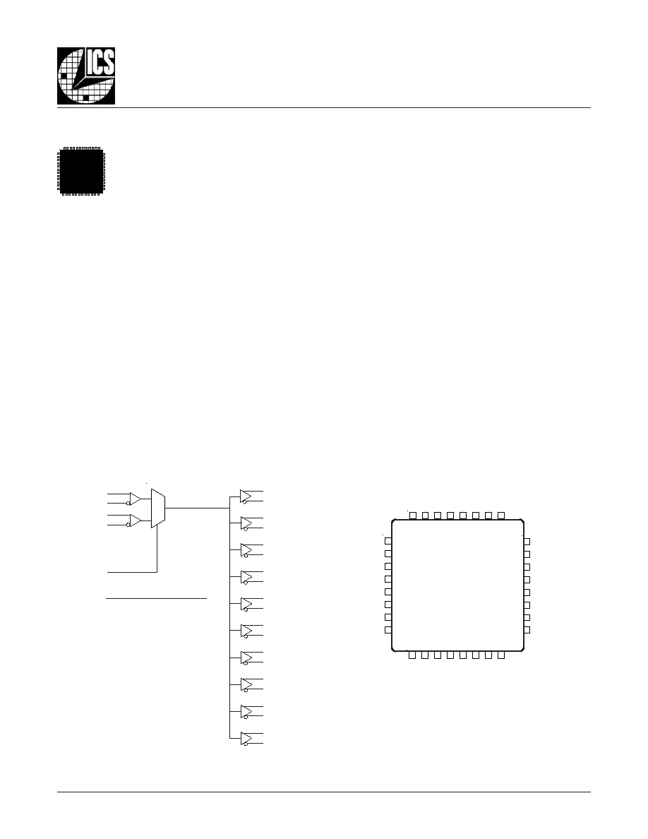
B
LOCK
D
IAGRAM
P
IN
A
SSIGNMENT
HiPerClockSTM
ICS
Q0
nQ0
Q1
nQ1
Q2
nQ2
Q3
nQ3
Q4
nQ4
Q5
nQ5
Q6
nQ6
Q7
nQ7
Q8
nQ8
Q9
nQ9
PCLK0
nPCLK0
0
1
PCLK1
nPCLK1
CLK_SEL
V
BB
The Preliminary Information presented herein represents a product in prototyping or pre-production. The noted characteristics are based on initial
product characterization. Integrated Circuit Systems, Incorporated (ICS) reserves the right to change any circuitry or specifications without notice.
32-Lead TQFP
7mm x 7mm x 1.0mm package body
Y Package
Top View
24 23 22 21 20 19 18 17
1 2 3 4 5 6 7 8
25
26
27
28
29
30
31
32
16
15
14
13
12
11
10
9
Q3
nQ3
Q4
nQ4
Q5
nQ5
Q6
nQ6
V
CCO
Q7
nQ7
Q8
nQ8
Q9
nQ9
V
CCO
V
CCO
nQ2
Q2
nQ1
Q1
nQ0
Q0
V
CCO
ICS853111-02
V
CC
CLK_SEL
PCLK0
nPCLK0
VBB
PCLK1
nPCLK
1
V
EE

853111AY-02
www.icst.com/products/hiperclocks.html
REV. A JANUARY 10, 2006
2
Integrated
Circuit
Systems, Inc.
ICS853111-02
L
OW
S
KEW
, 1-
TO
-10
D
IFFERENTIAL
-
TO
-2.5V/3.3V LVPECL/ECL F
ANOUT
B
UFFER
T
ABLE
1. P
IN
D
ESCRIPTIONS
T
ABLE
2. P
IN
C
HARACTERISTICS
T
ABLE
3B. C
ONTROL
I
NPUT
F
UNCTION
T
ABLE
T
ABLE
3A. C
LOCK
I
NPUT
F
UNCTION
T
ABLE
r
e
b
m
u
N
e
m
a
N
e
p
y
T
n
o
i
t
p
i
r
c
s
e
D
1
V
C
C
r
e
w
o
P
.
n
i
p
y
l
p
p
u
s
e
r
o
C
2
L
E
S
_
K
L
C
t
u
p
n
I
n
w
o
d
ll
u
P
.
s
t
u
p
n
i
1
K
L
C
P
n
,
1
K
L
C
P
s
t
c
e
l
e
s
,
H
G
I
H
n
e
h
W
.
t
u
p
n
i
t
c
e
l
e
s
k
c
o
l
C
.
s
t
u
p
n
i
0
K
L
C
P
n
,
0
K
L
C
P
s
t
c
e
l
e
s
,
W
O
L
n
e
h
W
.
s
l
e
v
e
l
e
c
a
f
r
e
t
n
i
L
T
T
V
L
/
S
O
M
C
V
L
3
0
K
L
C
P
t
u
p
n
I
n
w
o
d
ll
u
P
.
t
u
p
n
i
k
c
o
l
c
l
a
i
t
n
e
r
e
f
f
i
d
g
n
i
t
r
e
v
n
i
-
n
o
N
4
0
K
L
C
P
n
t
u
p
n
I
n
w
o
d
ll
u
P
/
p
u
ll
u
P
.
t
u
p
n
i
k
c
o
l
c
L
C
E
P
V
L
l
a
i
t
n
e
r
e
f
f
i
d
g
n
i
t
r
e
v
n
I
V
C
C
.
g
n
i
t
a
o
l
f
t
f
e
l
n
e
h
w
t
l
u
a
f
e
d
2
/
5
V
B
B
t
u
p
t
u
O
.
e
g
a
t
l
o
v
s
a
i
B
6
1
K
L
C
P
t
u
p
n
I
n
w
o
d
ll
u
P
.
t
u
p
n
i
k
c
o
l
c
l
a
i
t
n
e
r
e
f
f
i
d
g
n
i
t
r
e
v
n
i
-
n
o
N
7
1
K
L
C
P
n
t
u
p
n
I
n
w
o
d
ll
u
P
/
p
u
ll
u
P
.
t
u
p
n
i
k
c
o
l
c
L
C
E
P
V
L
l
a
i
t
n
e
r
e
f
f
i
d
g
n
i
t
r
e
v
n
I
V
C
C
.
g
n
i
t
a
o
l
f
t
f
e
l
n
e
h
w
t
l
u
a
f
e
d
2
/
8
V
E
E
r
e
w
o
P
.
n
i
p
y
l
p
p
u
s
e
v
i
t
a
g
e
N
2
3
,
5
2
,
6
1
,
9
V
O
C
C
r
e
w
o
P
.
s
n
i
p
y
l
p
p
u
s
t
u
p
t
u
O
1
1
,
0
1
9
Q
,
9
Q
n
t
u
p
t
u
O
.
s
l
e
v
e
l
e
c
a
f
r
e
t
n
i
L
C
E
P
V
L
.
r
i
a
p
t
u
p
t
u
o
l
a
i
t
n
e
r
e
f
f
i
D
3
1
,
2
1
8
Q
,
8
Q
n
t
u
p
t
u
O
.
s
l
e
v
e
l
e
c
a
f
r
e
t
n
i
L
C
E
P
V
L
.
r
i
a
p
t
u
p
t
u
o
l
a
i
t
n
e
r
e
f
f
i
D
5
1
,
4
1
7
Q
,
7
Q
n
t
u
p
t
u
O
.
s
l
e
v
e
l
e
c
a
f
r
e
t
n
i
L
C
E
P
V
L
.
r
i
a
p
t
u
p
t
u
o
l
a
i
t
n
e
r
e
f
f
i
D
8
1
,
7
1
6
Q
,
6
Q
n
t
u
p
t
u
O
.
s
l
e
v
e
l
e
c
a
f
r
e
t
n
i
L
C
E
P
V
L
.
r
i
a
p
t
u
p
t
u
o
l
a
i
t
n
e
r
e
f
f
i
D
0
2
,
9
1
5
Q
,
5
Q
n
t
u
p
t
u
O
.
s
l
e
v
e
l
e
c
a
f
r
e
t
n
i
L
C
E
P
V
L
.
r
i
a
p
t
u
p
t
u
o
l
a
i
t
n
e
r
e
f
f
i
D
2
2
,
1
2
4
Q
,
4
Q
n
t
u
p
t
u
O
.
s
l
e
v
e
l
e
c
a
f
r
e
t
n
i
L
C
E
P
V
L
.
r
i
a
p
t
u
p
t
u
o
l
a
i
t
n
e
r
e
f
f
i
D
4
2
,
3
2
3
Q
,
3
Q
n
t
u
p
t
u
O
.
s
l
e
v
e
l
e
c
a
f
r
e
t
n
i
L
C
E
P
V
L
.
r
i
a
p
t
u
p
t
u
o
l
a
i
t
n
e
r
e
f
f
i
D
7
2
,
6
2
2
Q
,
2
Q
n
t
u
p
t
u
O
.
s
l
e
v
e
l
e
c
a
f
r
e
t
n
i
L
C
E
P
V
L
.
r
i
a
p
t
u
p
t
u
o
l
a
i
t
n
e
r
e
f
f
i
D
9
2
,
8
2
1
Q
,
1
Q
n
t
u
p
t
u
O
.
s
l
e
v
e
l
e
c
a
f
r
e
t
n
i
L
C
E
P
V
L
.
r
i
a
p
t
u
p
t
u
o
l
a
i
t
n
e
r
e
f
f
i
D
1
3
,
0
3
0
Q
,
0
Q
n
t
u
p
t
u
O
.
s
l
e
v
e
l
e
c
a
f
r
e
t
n
i
L
C
E
P
V
L
.
r
i
a
p
t
u
p
t
u
o
l
a
i
t
n
e
r
e
f
f
i
D
:
E
T
O
N
n
w
o
d
ll
u
P
d
n
a
p
u
ll
u
P
.
s
e
u
l
a
v
l
a
c
i
p
y
t
r
o
f
,
s
c
i
t
s
i
r
e
t
c
a
r
a
h
C
n
i
P
,
2
e
l
b
a
T
e
e
S
.
s
r
o
t
s
i
s
e
r
t
u
p
n
i
l
a
n
r
e
t
n
i
o
t
r
e
f
e
r
l
o
b
m
y
S
r
e
t
e
m
a
r
a
P
s
n
o
i
t
i
d
n
o
C
t
s
e
T
m
u
m
i
n
i
M
l
a
c
i
p
y
T
m
u
m
i
x
a
M
s
t
i
n
U
R
N
W
O
D
L
L
U
P
r
o
t
s
i
s
e
R
n
w
o
d
ll
u
P
t
u
p
n
I
5
7
k
R
/
C
C
V
2
s
r
o
t
s
i
s
e
R
n
w
o
d
ll
u
P
/
p
u
ll
u
P
0
5
k
s
t
u
p
n
I
s
t
u
p
t
u
O
e
d
o
M
t
u
p
t
u
O
o
t
t
u
p
n
I
y
t
i
r
a
l
o
P
x
K
L
C
P
x
K
L
C
P
n
9
Q
:
0
Q
9
Q
:
0
Q
n
0
1
W
O
L
H
G
I
H
l
a
i
t
n
e
r
e
f
f
i
D
o
t
l
a
i
t
n
e
r
e
f
f
i
D
g
n
i
t
r
e
v
n
I
n
o
N
1
0
H
G
I
H
W
O
L
l
a
i
t
n
e
r
e
f
f
i
D
o
t
l
a
i
t
n
e
r
e
f
f
i
D
g
n
i
t
r
e
v
n
I
n
o
N
0
;
d
e
s
a
i
B
1
E
T
O
N
W
O
L
H
G
I
H
l
a
i
t
n
e
r
e
f
f
i
D
o
t
d
e
d
n
E
e
l
g
n
i
S
g
n
i
t
r
e
v
n
I
n
o
N
1
;
d
e
s
a
i
B
1
E
T
O
N
H
G
I
H
W
O
L
l
a
i
t
n
e
r
e
f
f
i
D
o
t
d
e
d
n
E
e
l
g
n
i
S
g
n
i
t
r
e
v
n
I
n
o
N
;
d
e
s
a
i
B
1
E
T
O
N
0
H
G
I
H
W
O
L
l
a
i
t
n
e
r
e
f
f
i
D
o
t
d
e
d
n
E
e
l
g
n
i
S
g
n
i
t
r
e
v
n
I
;
d
e
s
a
i
B
1
E
T
O
N
1
W
O
L
H
G
I
H
l
a
i
t
n
e
r
e
f
f
i
D
o
t
d
e
d
n
E
e
l
g
n
i
S
g
n
i
t
r
e
v
n
I
o
t
t
u
p
n
I
l
a
i
t
n
e
r
e
f
f
i
D
e
h
t
g
n
i
r
i
W
"
,
n
o
i
t
a
m
r
o
f
n
I
n
o
i
t
a
c
il
p
p
A
e
h
t
o
t
r
e
f
e
r
e
s
a
e
l
P
:
1
E
T
O
N
.
"
s
l
e
v
e
L
d
e
d
n
E
e
l
g
n
i
S
t
p
e
c
c
A
s
t
u
p
n
I
L
E
S
_
K
L
C
e
c
r
u
o
S
d
e
t
c
e
l
e
S
0
0
K
L
C
P
n
,
0
K
L
C
P
1
1
K
L
C
P
n
,
1
K
L
C
P
853111AY-02
www.icst.com/products/hiperclocks.html
REV. A JANUARY 10, 2006
3
Integrated
Circuit
Systems, Inc.
ICS853111-02
L
OW
S
KEW
, 1-
TO
-10
D
IFFERENTIAL
-
TO
-2.5V/3.3V LVPECL/ECL F
ANOUT
B
UFFER
T
ABLE
4A. P
OWER
S
UPPLY
DC C
HARACTERISTICS
,
V
CC
= 2.375
TO
3.8V; V
EE
= 0V
l
o
b
m
y
S
r
e
t
e
m
a
r
a
P
s
n
o
i
t
i
d
n
o
C
t
s
e
T
m
u
m
i
n
i
M
l
a
c
i
p
y
T
m
u
m
i
x
a
M
s
t
i
n
U
V
C
C
e
g
a
t
l
o
V
y
l
p
p
u
S
e
v
i
t
i
s
o
P
5
7
3
.
2
3
.
3
8
.
3
V
I
E
E
t
n
e
r
r
u
C
y
l
p
p
u
S
r
e
w
o
P
5
8
A
m
T
ABLE
4B. LVPECL DC C
HARACTERISTICS
,
V
CC
= 3.3V; V
EE
= 0V
l
o
b
m
y
S
r
e
t
e
m
a
r
a
P
C
�
0
4
-
C
�
5
2
C
�
5
8
s
t
i
n
U
n
i
M
p
y
T
x
a
M
n
i
M
p
y
T
x
a
M
n
i
M
p
y
T
x
a
M
V
H
O
1
E
T
O
N
;
e
g
a
t
l
o
V
h
g
i
H
t
u
p
t
u
O
5
7
1
.
2
5
7
2
.
2
8
3
.
2
5
2
2
.
2
5
9
2
.
2
7
3
.
2
5
9
2
.
2
3
3
.
2
5
6
3
.
2
V
V
L
O
1
E
T
O
N
;
e
g
a
t
l
o
V
w
o
L
t
u
p
t
u
O
5
0
4
.
1
5
4
5
.
1
8
6
.
1
5
2
4
.
1
2
5
.
1
5
1
6
.
1
4
4
.
1
5
3
5
.
1
3
6
.
1
V
V
H
I
e
g
a
t
l
o
V
h
g
i
H
t
u
p
n
I
)
d
e
d
n
E
-
e
l
g
n
i
S
(
5
7
0
.
2
6
3
.
2
5
7
0
.
2
6
3
.
2
5
7
0
.
2
6
3
.
2
V
V
L
I
e
g
a
t
l
o
V
w
o
L
t
u
p
n
I
)
d
e
d
n
E
-
e
l
g
n
i
S
(
3
4
.
1
5
6
7
.
1
3
4
.
1
5
6
7
.
1
3
4
.
1
5
6
7
.
1
V
V
B
B
2
E
T
O
N
;
e
c
n
e
r
e
f
e
R
e
g
a
t
l
o
V
t
u
p
t
u
O
6
8
.
1
8
9
.
1
6
8
.
1
8
9
.
1
6
8
.
1
8
9
.
1
V
V
P
P
e
g
a
t
l
o
V
t
u
p
n
I
k
a
e
P
-
o
t
-
k
a
e
P
0
5
1
0
0
8
0
0
2
1
0
5
1
0
0
8
0
0
2
1
0
5
1
0
0
8
0
0
2
1
V
V
R
M
C
e
g
a
t
l
o
V
h
g
i
H
t
u
p
n
I
4
,
3
E
T
O
N
;
e
g
n
a
R
e
d
o
M
n
o
m
m
o
C
2
.
1
3
.
3
2
.
1
3
.
3
2
.
1
3
.
3
V
I
H
I
t
n
e
r
r
u
C
h
g
i
H
t
u
p
n
I
1
K
L
C
P
,
0
K
L
C
P
1
K
L
C
P
n
,
0
K
L
C
P
n
0
5
1
0
5
1
0
5
1
A
�
I
L
I
t
n
e
r
r
u
C
w
o
L
t
u
p
n
I
1
K
L
C
P
,
0
K
L
C
P
1
K
L
C
P
n
,
0
K
L
C
P
n
0
5
1
-
0
5
1
-
0
5
1
-
A
�
V
h
t
i
w
1
:
1
y
r
a
v
s
r
e
t
e
m
a
r
a
p
t
u
p
t
u
o
d
n
a
t
u
p
n
I
C
C
V
.
E
E
.
V
5
.
0
-
o
t
V
5
2
9
.
0
+
y
r
a
v
n
a
c
0
5
h
t
i
w
d
e
t
a
n
i
m
r
e
t
s
t
u
p
t
u
O
:
1
E
T
O
N
V
o
t
O
C
C
.
V
2
-
V
d
e
t
i
m
il
s
i
n
o
i
t
a
r
e
p
o
t
u
p
n
i
d
e
d
n
e
-
e
l
g
n
i
S
:
2
E
T
O
N
C
C
.
e
d
o
m
L
C
E
P
V
L
n
i
V
3
V
s
a
d
e
n
i
f
e
d
s
i
e
g
a
t
l
o
v
e
d
o
m
n
o
m
m
o
C
:
3
E
T
O
N
H
I
.
1
K
L
C
P
n
,
1
K
L
C
P
d
n
a
0
K
L
C
P
n
,
0
K
L
C
P
r
o
f
e
g
a
t
l
o
v
t
u
p
n
i
m
u
m
i
x
a
m
e
h
t
,
s
n
o
i
t
a
c
il
p
p
a
d
e
d
n
e
-
e
l
g
n
i
s
r
o
F
:
4
E
T
O
N
V
s
i
C
C
.
V
3
.
0
+
A
BSOLUTE
M
AXIMUM
R
ATINGS
Supply Voltage, V
CC
4.6V (LVPECL mode, V
EE
= 0)
Negative Supply Voltage, V
EE
-4.6V (ECL mode, V
CC
= 0)
Inputs, V
I
(LVPECL mode)
-0.5V to V
CC
+ 0.5 V
Inputs, V
I
(ECL mode)
0.5V to V
EE
- 0.5V
Outputs, I
O
Continuous Current
50mA
Surge Current
100mA
V
BB
Sink/Source, I
BB
� 0.5mA
Operating Temperature Range, TA -40�C to +85�C
Storage Temperature, T
STG
-65�C to 150�C
Package Thermal Impedance,
JA
49.5�C/W (0 lfpm)
(Junction-to-Ambient)
NOTE: Stresses beyond those listed under Absolute
Maximum Ratings may cause permanent damage
to the device. These ratings are stress specifi-
cations only. Functional operation of product at
these conditions or any conditions beyond those
listed in the
DC Characteristics
or
AC Character-
istics
is not implied. Exposure to absolute maxi-
mum rating conditions for extended periods may
affect product reliability.
853111AY-02
www.icst.com/products/hiperclocks.html
REV. A JANUARY 10, 2006
4
Integrated
Circuit
Systems, Inc.
ICS853111-02
L
OW
S
KEW
, 1-
TO
-10
D
IFFERENTIAL
-
TO
-2.5V/3.3V LVPECL/ECL F
ANOUT
B
UFFER
T
ABLE
4D. ECL DC C
HARACTERISTICS
,
V
CC
= 0V; V
EE
= -3.8V
TO
-2.375V
T
ABLE
4C. LVPECL DC C
HARACTERISTICS
,
V
CC
= 2.5V; V
EE
= 0V
l
o
b
m
y
S
r
e
t
e
m
a
r
a
P
C
�
0
4
-
C
�
5
2
C
�
5
8
s
t
i
n
U
n
i
M
p
y
T
x
a
M
n
i
M
p
y
T
x
a
M
n
i
M
p
y
T
x
a
M
V
H
O
1
E
T
O
N
;
e
g
a
t
l
o
V
h
g
i
H
t
u
p
t
u
O
5
7
3
.
1
5
7
4
.
1
8
5
.
1
5
2
4
.
1
5
9
4
.
1
7
5
.
1
5
9
4
.
1
3
5
.
1
5
6
5
.
1
V
V
L
O
1
E
T
O
N
;
e
g
a
t
l
o
V
w
o
L
t
u
p
t
u
O
5
0
6
.
0
5
4
7
.
0
8
8
.
0
5
2
6
.
0
2
7
.
0
5
1
8
.
0
4
6
.
0
5
3
7
.
0
3
8
.
0
V
V
H
I
e
g
a
t
l
o
V
h
g
i
H
t
u
p
n
I
)
d
e
d
n
E
-
e
l
g
n
i
S
(
5
7
2
.
1
6
5
.
1
5
7
2
.
1
6
5
.
1
5
7
2
.
1
8
.
0
-
V
V
L
I
e
g
a
t
l
o
V
w
o
L
t
u
p
n
I
)
d
e
d
n
E
-
e
l
g
n
i
S
(
3
6
.
0
5
6
9
.
0
3
6
.
0
5
6
9
.
0
3
6
.
0
5
6
9
.
0
V
V
P
P
e
g
a
t
l
o
V
t
u
p
n
I
k
a
e
P
-
o
t
-
k
a
e
P
0
5
1
0
0
8
0
0
2
1
0
5
1
0
0
8
0
0
2
1
0
5
1
0
0
8
0
0
2
1
V
V
R
M
C
e
g
a
t
l
o
V
h
g
i
H
t
u
p
n
I
3
,
2
E
T
O
N
;
e
g
n
a
R
e
d
o
M
n
o
m
m
o
C
2
.
1
5
.
2
2
.
1
5
.
2
2
.
1
5
.
2
V
I
H
I
t
n
e
r
r
u
C
h
g
i
H
t
u
p
n
I
1
K
L
C
P
,
0
K
L
C
P
1
K
L
C
P
n
,
0
K
L
C
P
n
0
5
1
0
5
1
0
5
1
A
�
I
L
I
t
n
e
r
r
u
C
w
o
L
t
u
p
n
I
1
K
L
C
P
,
0
K
L
C
P
1
K
L
C
P
n
,
0
K
L
C
P
n
0
5
1
-
0
5
1
-
0
5
1
-
A
�
V
h
t
i
w
1
:
1
y
r
a
v
s
r
e
t
e
m
a
r
a
p
t
u
p
t
u
o
d
n
a
t
u
p
n
I
C
C
V
.
E
E
.
V
3
.
1
-
o
t
V
5
2
1
.
0
+
y
r
a
v
n
a
c
0
5
h
t
i
w
d
e
t
a
n
i
m
r
e
t
s
t
u
p
t
u
O
:
1
E
T
O
N
V
o
t
O
C
C
.
V
2
-
V
s
a
d
e
n
i
f
e
d
s
i
e
g
a
t
l
o
v
e
d
o
m
n
o
m
m
o
C
:
2
E
T
O
N
H
I
.
1
K
L
C
P
n
,
1
K
L
C
P
d
n
a
0
K
L
C
P
n
,
0
K
L
C
P
r
o
f
e
g
a
t
l
o
v
t
u
p
n
i
m
u
m
i
x
a
m
e
h
t
,
s
n
o
i
t
a
c
il
p
p
a
d
e
d
n
e
-
e
l
g
n
i
s
r
o
F
:
3
E
T
O
N
V
s
i
C
C
.
V
3
.
0
+
l
o
b
m
y
S
r
e
t
e
m
a
r
a
P
C
�
0
4
-
C
�
5
2
C
�
5
8
s
t
i
n
U
n
i
M
p
y
T
x
a
M
n
i
M
p
y
T
x
a
M
n
i
M
p
y
T
x
a
M
V
H
O
1
E
T
O
N
;
e
g
a
t
l
o
V
h
g
i
H
t
u
p
t
u
O
5
2
1
.
1
-
5
2
0
.
1
-
2
9
.
0
-
5
7
0
.
1
-
5
0
0
.
1
-
3
9
.
0
-
5
0
0
.
1
-
7
9
.
0
-
5
3
9
.
0
-
V
V
L
O
1
E
T
O
N
;
e
g
a
t
l
o
V
w
o
L
t
u
p
t
u
O
5
9
8
.
1
-
5
5
7
.
1
-
2
6
.
1
-
5
7
8
.
1
-
8
7
.
1
-
5
8
6
.
1
-
6
8
.
1
-
5
6
7
.
1
-
7
6
.
1
-
V
V
H
I
e
g
a
t
l
o
V
h
g
i
H
t
u
p
n
I
)
d
e
d
n
E
-
e
l
g
n
i
S
(
5
2
2
.
1
-
4
9
.
0
-
5
2
2
.
1
-
4
9
.
0
-
5
2
2
.
1
-
4
9
.
0
-
V
V
L
I
e
g
a
t
l
o
V
w
o
L
t
u
p
n
I
)
d
e
d
n
E
-
e
l
g
n
i
S
(
7
8
.
1
-
5
3
5
.
1
-
7
8
.
1
-
5
3
5
.
1
-
7
8
.
1
-
5
3
5
.
1
-
V
V
B
B
;
e
c
n
e
r
e
f
e
R
e
g
a
t
l
o
V
t
u
p
t
u
O
2
E
T
O
N
6
8
4
.
1
-
6
8
3
.
1
-
6
8
4
.
1
-
6
8
3
.
1
-
6
8
4
.
1
-
6
8
3
.
1
-
V
V
P
P
e
g
a
t
l
o
V
t
u
p
n
I
k
a
e
P
-
o
t
-
k
a
e
P
0
5
1
0
0
8
0
0
2
1
0
5
1
0
0
8
0
0
2
1
0
5
1
0
0
8
0
0
2
1
V
V
R
M
C
e
g
a
t
l
o
V
h
g
i
H
t
u
p
n
I
;
e
g
n
a
R
e
d
o
M
n
o
m
m
o
C
4
,
3
E
T
O
N
V
E
E
V
2
.
1
+
0
V
E
E
V
2
.
1
+
0
V
E
E
V
2
.
1
+
0
V
I
H
I
t
u
p
n
I
t
n
e
r
r
u
C
h
g
i
H
1
K
L
C
P
,
0
K
L
C
P
1
K
L
C
P
n
,
0
K
L
C
P
n
0
5
1
0
5
1
0
5
1
A
�
I
L
I
t
u
p
n
I
t
n
e
r
r
u
C
w
o
L
1
K
L
C
P
,
0
K
L
C
P
1
K
L
C
P
n
,
0
K
L
C
P
n
0
5
1
-
0
5
1
-
0
5
1
-
A
�
V
h
t
i
w
1
:
1
y
r
a
v
s
r
e
t
e
m
a
r
a
p
t
u
p
t
u
o
d
n
a
t
u
p
n
I
C
C
V
.
E
E
.
V
5
.
0
-
o
t
V
5
2
9
.
0
+
y
r
a
v
n
a
c
0
5
h
t
i
w
d
e
t
a
n
i
m
r
e
t
s
t
u
p
t
u
O
:
1
E
T
O
N
V
o
t
O
C
C
.
V
2
-
V
d
e
t
i
m
il
s
i
n
o
i
t
a
r
e
p
o
t
u
p
n
i
d
e
d
n
e
-
e
l
g
n
i
S
:
2
E
T
O
N
C
C
.
e
d
o
m
L
C
E
P
V
L
n
i
V
3
V
s
a
d
e
n
i
f
e
d
s
i
e
g
a
t
l
o
v
e
d
o
m
n
o
m
m
o
C
:
3
E
T
O
N
H
I
.
1
K
L
C
P
n
,
1
K
L
C
P
d
n
a
0
K
L
C
P
n
,
0
K
L
C
P
r
o
f
e
g
a
t
l
o
v
t
u
p
n
i
m
u
m
i
x
a
m
e
h
t
,
s
n
o
i
t
a
c
il
p
p
a
d
e
d
n
e
-
e
l
g
n
i
s
r
o
F
:
4
E
T
O
N
V
s
i
C
C
.
V
3
.
0
+

853111AY-02
www.icst.com/products/hiperclocks.html
REV. A JANUARY 10, 2006
5
Integrated
Circuit
Systems, Inc.
ICS853111-02
L
OW
S
KEW
, 1-
TO
-10
D
IFFERENTIAL
-
TO
-2.5V/3.3V LVPECL/ECL F
ANOUT
B
UFFER
T
ABLE
5. AC C
HARACTERISTICS
,
V
CC
= 0V; V
EE
= -3.8V
TO
-2.375V
OR
V
CC
= 2.375
TO
3.8V; V
EE
= 0V
l
o
b
m
y
S
r
e
t
e
m
a
r
a
P
C
�
0
4
-
C
�
5
2
C
�
5
8
s
t
i
n
U
n
i
M
p
y
T
x
a
M
n
i
M
p
y
T
x
a
M
n
i
M
p
y
T
x
a
M
f
X
A
M
y
c
n
e
u
q
e
r
F
t
u
p
t
u
O
2
.
3
2
.
3
2
.
3
z
H
G
t
D
P
1
E
T
O
N
;
y
a
l
e
D
n
o
i
t
a
g
a
p
o
r
P
0
0
6
0
8
6
0
5
7
0
5
6
5
2
7
0
9
7
0
9
6
0
9
7
0
9
8
s
p
t
)
o
(
k
s
4
,
2
E
T
O
N
;
w
e
k
S
t
u
p
t
u
O
5
2
7
3
5
2
7
3
5
2
7
3
s
p
t
)
p
p
(
k
s
4
,
3
E
T
O
N
;
w
e
k
S
t
r
a
P
-
o
t
-
t
r
a
P
5
8
5
2
2
5
8
5
2
2
5
8
5
2
2
s
p
t
t
ij
;
S
M
R
,
r
e
t
t
i
J
e
s
a
h
P
e
v
i
t
i
d
d
A
r
e
f
f
u
B
n
o
i
t
c
e
s
r
e
t
t
i
J
e
s
a
h
P
e
v
i
t
i
d
d
A
o
t
r
e
f
e
r
3
0
.
0
3
0
.
0
3
0
.
0
s
p
t
R
/t
F
e
m
i
T
ll
a
F
/
e
s
i
R
t
u
p
t
u
O
%
0
8
o
t
%
0
2
0
6
0
0
2
5
2
3
0
0
1
0
0
2
0
8
2
0
3
1
0
0
2
0
7
2
s
p
d
e
r
u
s
a
e
m
e
r
a
s
r
e
t
e
m
a
r
a
p
ll
A
.
d
e
t
o
n
e
s
i
w
r
e
h
t
o
s
s
e
l
n
u
z
H
G
1
.
t
n
i
o
p
g
n
i
s
s
o
r
c
t
u
p
t
u
o
l
a
i
t
n
e
r
e
f
f
i
d
e
h
t
o
t
t
n
i
o
p
g
n
i
s
s
o
r
c
t
u
p
n
i
l
a
i
t
n
e
r
e
f
f
i
d
e
h
t
m
o
r
f
d
e
r
u
s
a
e
M
:
1
E
T
O
N
.
s
n
o
i
t
i
d
n
o
c
d
a
o
l
l
a
u
q
e
h
t
i
w
d
n
a
e
g
a
t
l
o
v
y
l
p
p
u
s
e
m
a
s
e
h
t
t
a
s
t
u
p
t
u
o
n
e
e
w
t
e
b
w
e
k
s
s
a
d
e
n
i
f
e
D
:
2
E
T
O
N
.
s
t
n
i
o
p
s
s
o
r
c
l
a
i
t
n
e
r
e
f
f
i
d
t
u
p
t
u
o
e
h
t
t
a
d
e
r
u
s
a
e
M
s
e
g
a
t
l
o
v
y
l
p
p
u
s
e
m
a
s
e
h
t
t
a
g
n
i
t
a
r
e
p
o
s
e
c
i
v
e
d
t
n
e
r
e
f
f
i
d
n
o
s
t
u
p
t
u
o
n
e
e
w
t
e
b
w
e
k
s
s
a
d
e
n
i
f
e
D
:
3
E
T
O
N
d
e
r
u
s
a
e
m
e
r
a
s
t
u
p
t
u
o
e
h
t
,
e
c
i
v
e
d
h
c
a
e
n
o
s
t
u
p
n
i
f
o
e
p
y
t
e
m
a
s
e
h
t
g
n
i
s
U
.
s
n
o
i
t
i
d
n
o
c
d
a
o
l
l
a
u
q
e
h
t
i
w
d
n
a
.
s
t
n
i
o
p
s
s
o
r
c
l
a
i
t
n
e
r
e
f
f
i
d
e
h
t
t
a
.
5
6
d
r
a
d
n
a
t
S
C
E
D
E
J
h
t
i
w
e
c
n
a
d
r
o
c
c
a
n
i
d
e
n
i
f
e
d
s
i
r
e
t
e
m
a
r
a
p
s
i
h
T
:
4
E
T
O
N
853111AY-02
www.icst.com/products/hiperclocks.html
REV. A JANUARY 10, 2006
6
Integrated
Circuit
Systems, Inc.
ICS853111-02
L
OW
S
KEW
, 1-
TO
-10
D
IFFERENTIAL
-
TO
-2.5V/3.3V LVPECL/ECL F
ANOUT
B
UFFER
A
DDITIVE
P
HASE
J
ITTER
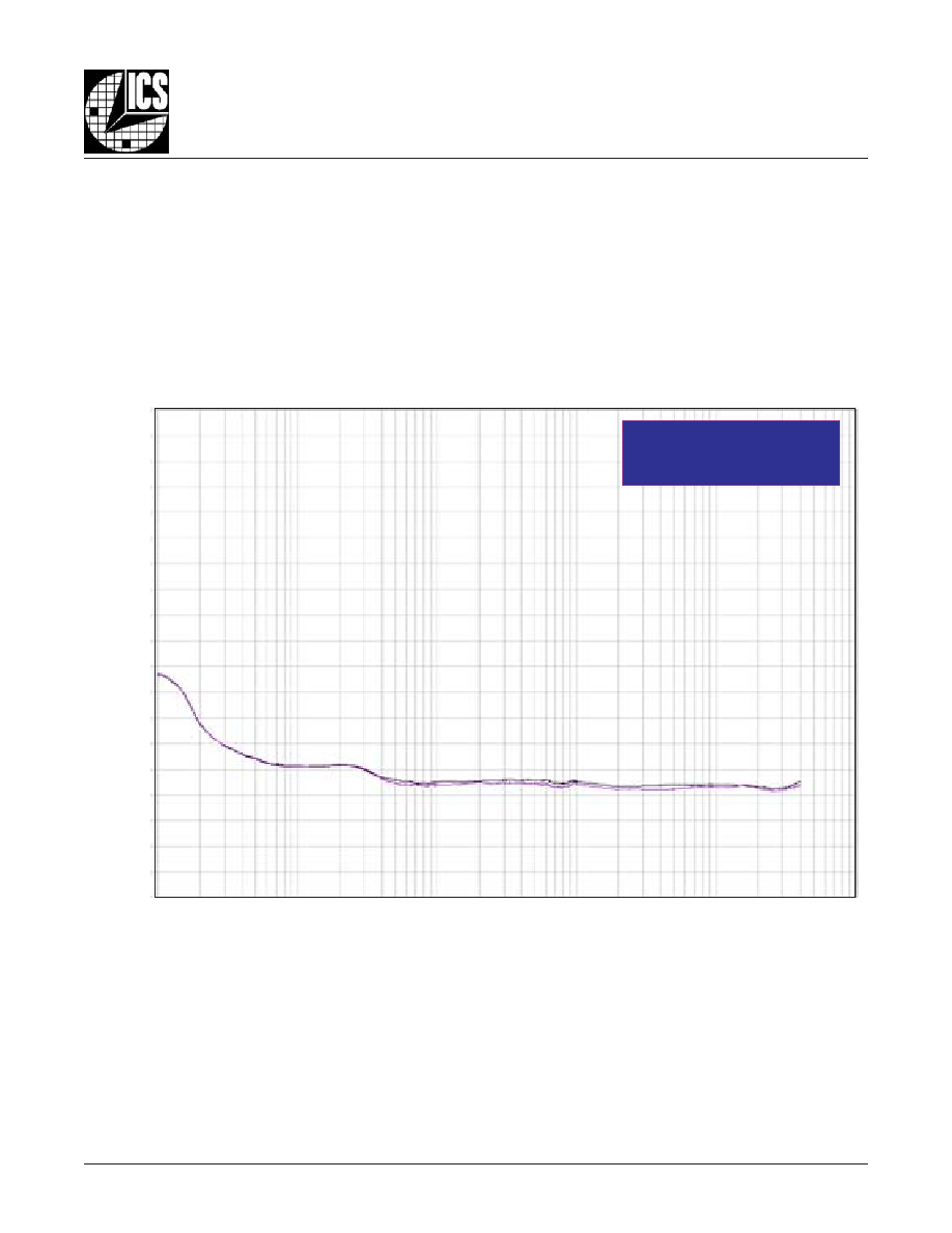
The spectral purity in a band at a specific offset from the funda-
mental compared to the power of the fundamental is called the
dBc Phase Noise.
This value is normally expressed using a
Phase noise plot and is most often the specified plot in many
applications. Phase noise is defined as the ratio of the noise
power present in a 1Hz band at a specified offset from the fun-
damental frequency to the power value of the fundamental. This
ratio is expressed in decibels (dBm) or a ratio of the power in
As with most timing specifications, phase noise measurements
have issues. The primary issue relates to the limitations of the
equipment. Often the noise floor of the equipment is higher than
the noise floor of the device. This is illustrated above. The de-
the 1Hz band to the power in the fundamental. When the re-
quired offset is specified, the phase noise is called a
dBc
value,
which simply means dBm at a specified offset from the funda-
mental. By investigating jitter in the frequency domain, we get a
better understanding of its effects on the desired application over
the entire time record of the signal. It is mathematically possible
to calculate an expected bit error rate given a phase noise plot.
vice meets the noise floor of what is shown, but can actually be
lower. The phase noise is dependant on the input source and
measurement equipment.
Additive Phase Jitter
at
155.52MHz = 0.03ps (typical)
0
-10
-20
-30
-40
-50
-60
-70
-80
-90
-100
-110
-120
-130
-140
-150
-160
-170
-180
-190
1k
10k
100k
1M
10M
100M
O
FFSET
F
ROM
C
ARRIER
F
REQUENCY
(H
Z
)
SSB P
HASE
N
OISE
dBc/H
Z
853111AY-02
www.icst.com/products/hiperclocks.html
REV. A JANUARY 10, 2006
7
Integrated
Circuit
Systems, Inc.
ICS853111-02
L
OW
S
KEW
, 1-
TO
-10
D
IFFERENTIAL
-
TO
-2.5V/3.3V LVPECL/ECL F
ANOUT
B
UFFER
P
ARAMETER
M
EASUREMENT
I
NFORMATION
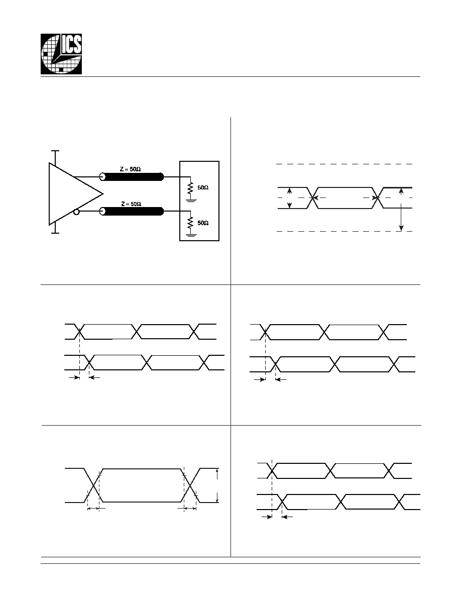
3.3V O
UTPUT
L
OAD
AC T
EST
C
IRCUIT
D
IFFERENTIAL
I
NPUT
L
EVEL
O
UTPUT
S
KEW
P
ART
-
TO
-P
ART
S
KEW
O
UTPUT
R
ISE
/F
ALL
T
IME
P
ROPAGATION
D
ELAY
V
CMR
Cross Points
V
PP
V
EE
nCLK0, nCLK1
V
CC
CLK0, CLK1
SCOPE
Qx
nQx
LVPECL
V
CC
,
V
CCO
-0.375V to -1.8V
t
sk(pp)
t
sk(o)
nQx
Qx
nQy
Qy
PART 1
PART 2
nQx
Qx
nQy
Qy
Clock
Outputs
20%
80%
80%
20%
t
R
t
F
V
SW I N G
t
PD
nCLK0,
nCLK1
Q0:Q9
nQ0:nQ9
CLK0,
CLK1
2V
V
EE
853111AY-02
www.icst.com/products/hiperclocks.html
REV. A JANUARY 10, 2006
8
Integrated
Circuit
Systems, Inc.
ICS853111-02
L
OW
S
KEW
, 1-
TO
-10
D
IFFERENTIAL
-
TO
-2.5V/3.3V LVPECL/ECL F
ANOUT
B
UFFER
F
IGURE
2A. S
INGLE
E
NDED
LVCMOS S
IGNAL
D
RIVING
D
IFFERENTIAL
I
NPUT
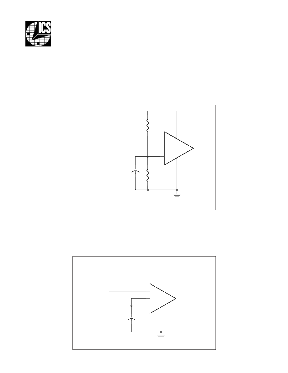
Figure 2A
shows an example of the differential input that
can be wired to accept single ended LVCMOS levels. The
reference voltage level V
BB
generated from the device is
A
PPLICATION
I
NFORMATION
W
IRING
THE
D
IFFERENTIAL
I
NPUT
TO
A
CCEPT
S
INGLE
E
NDED
LVCMOS L
EVELS
connected to the negative input. The C1 capacitor should
be located as close as possible to the input pin.
F
IGURE
2B. S
INGLE
E
NDED
LVPECL S
IGNAL
D
RIVING
D
IFFERENTIAL
I
NPUT
Figure 2B
shows an example of the differential input that
can be wired to accept single ended LVPECL levels. The
reference voltage level V
BB
generated from the device is
connected to the negative input. The C1 capacitor should
be located as close as possible to the input pin.
W
IRING
THE
D
IFFERENTIAL
I
NPUT
TO
A
CCEPT
S
INGLE
E
NDED
LVPECL L
EVELS
CLK_IN
C1
0.1uF
VDD(or VCC)
+
-
VBB
VCC
R2
1K
V_REF
C1
0.1u
R1
1K
Single Ended Clock Input
PCLK
nPCLK
853111AY-02
www.icst.com/products/hiperclocks.html
REV. A JANUARY 10, 2006
9
Integrated
Circuit
Systems, Inc.
ICS853111-02
L
OW
S
KEW
, 1-
TO
-10
D
IFFERENTIAL
-
TO
-2.5V/3.3V LVPECL/ECL F
ANOUT
B
UFFER
LVPECL C
LOCK
I
NPUT
I
NTERFACE
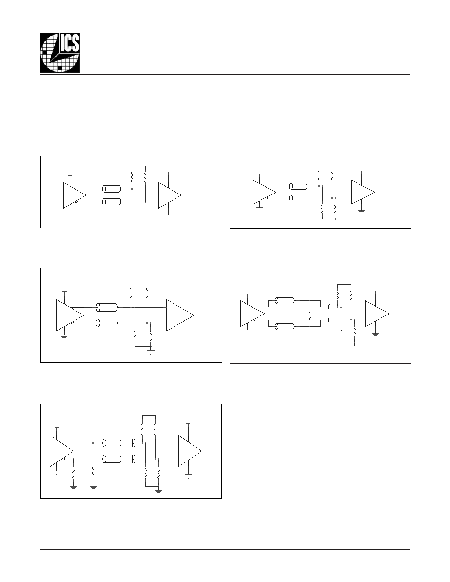
The PCLK /nPCLK accepts LVPECL, CML, SSTL and other
differential signals. Both V
SWING
and V
OH
must meet the V
PP
and V
CMR
input requirements.
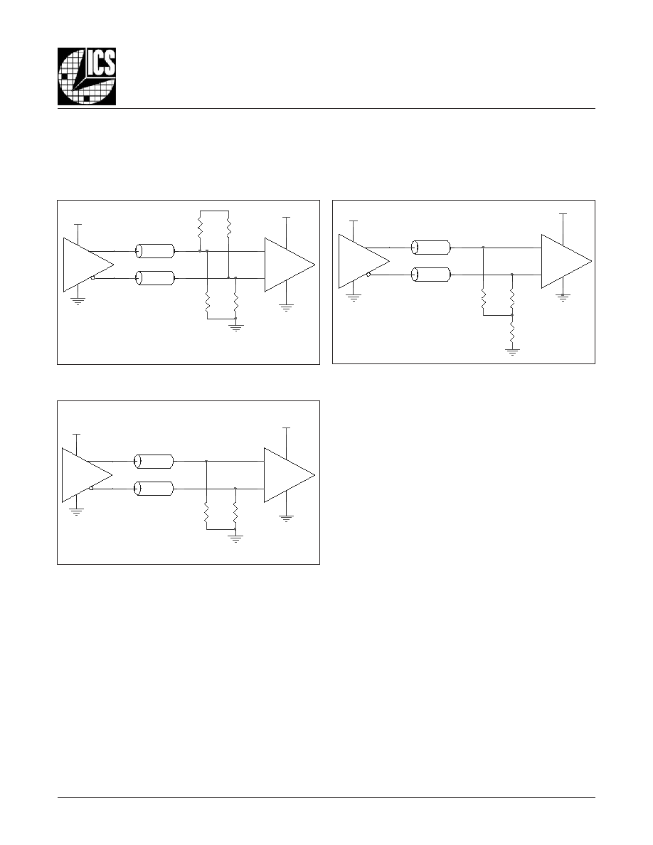
Figures 3A to 3E
show inter-
face examples for the HiPerClockS PCLK/nPCLK input driven
by the most common driver types. The input interfaces sug-
gested here are examples only. If the driver is from another
vendor, use their termination recommendation. Please con-
sult with the vendor of the driver component to confirm the
driver termination requirements.
F
IGURE
3A. H
I
P
ER
C
LOCK
S PCLK/
N
PCLK I
NPUT
D
RIVEN
BY
A
CML D
RIVER
F
IGURE
3B. H
I
P
ER
C
LOCK
S PCLK/
N
PCLK I
NPUT
D
RIVEN
BY
AN
SSTL D
RIVER
F
IGURE
3C. H
I
P
ER
C
LOCK
S PCLK/
N
PCLK I
NPUT
D
RIVEN
BY
A
3.3V LVPECL D
RIVER
F
IGURE
3D. H
I
P
ER
C
LOCK
S PCLK/
N
PCLK I
NPUT
D
RIVEN
BY
A
3.3V LVDS D
RIVER
HiPerClockS
PCLK
nPCLK
PCLK/nPCLK
3.3V
R2
50
R1
50
3.3V
Zo = 50 Ohm
CML
3.3V
Zo = 50 Ohm
PCLK/nPCLK
2.5V
Zo = 60 Ohm
SSTL
HiPerClockS
PCLK
nPCLK
R2
120
3.3V
R3
120
Zo = 60 Ohm
R1
120
R4
120
2.5V
Zo = 50 Ohm
Input
HiPerClockS
CLK
nCLK
3.3V
R3
125
R2
84
Zo = 50 Ohm
3.3V
R4
125
LVPECL
R1
84
3.3V
F
IGURE
3E. H
I
P
ER
C
LOCK
S PCLK/
N
PCLK I
NPUT
D
RIVEN
BY
A
3.3V LVPECL D
RIVER
WITH
AC C
OUPLE
3.3V
R5
100 - 200
3.3V
3.3V
HiPerClockS
PCLK
nPCLK
R1
125
PCLK/nPCLK
R2
125
R3
84
C1
C2
Zo = 50 Ohm
R4
84
Zo = 50 Ohm
R6
100 - 200
3.3V LVPECL
C2
R2
1K
R5
100
Zo = 50 Ohm
3.3V
3.3V
C1
R3
1K
LVDS
R4
1K
HiPerClockS
PCLK
nPCLK
R1
1K
Zo = 50 Ohm
3.3V
PC L K /n PC LK
853111AY-02
www.icst.com/products/hiperclocks.html
REV. A JANUARY 10, 2006
10
Integrated
Circuit
Systems, Inc.
ICS853111-02
L
OW
S
KEW
, 1-
TO
-10
D
IFFERENTIAL
-
TO
-2.5V/3.3V LVPECL/ECL F
ANOUT
B
UFFER
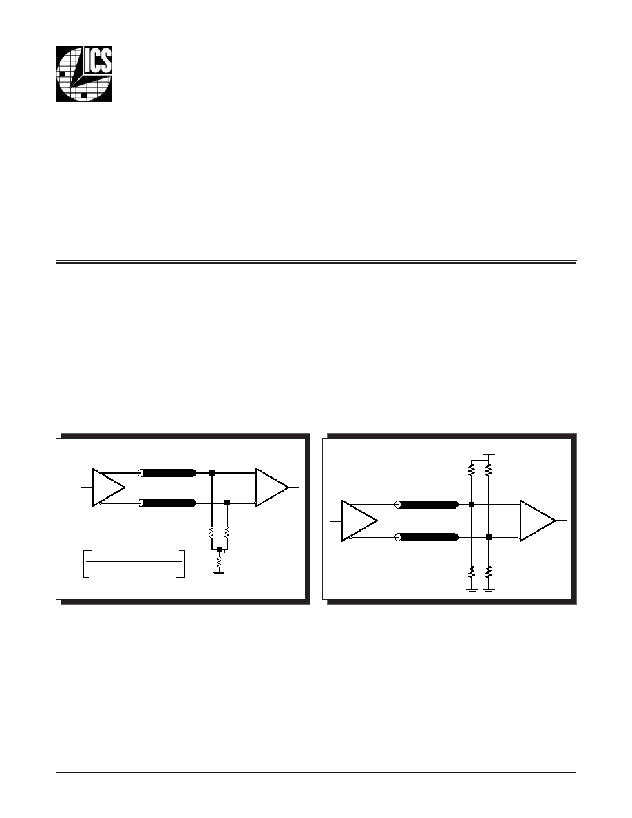
V
CC
- 2V
50
50
RTT
Z
o
= 50
Z
o
= 50
FOUT
FIN
RTT =
Z
o
1
((V
OH
+ V
OL
) / (V
CC
� 2)) � 2
3.3V
125
125
84
84
Z
o
= 50
Z
o
= 50
FOUT
FIN
The clock layout topology shown below is a typical termi-
nation for LVPECL outputs. The two different layouts men-
tioned are recommended only as guidelines.
FOUT and nFOUT are low impedance follower outputs that
generate ECL/LVPECL compatible outputs. Therefore, ter-
minating resistors (DC current path to ground) or current
sources must be used for functionality. These outputs are
designed to drive 50
transmission lines. Matched imped-
ance techniques should be used to maximize operating
frequency and minimize signal distortion.
Figures 4A and
4B
show two different layouts which are recommended only
as guidelines. Other suitable clock layouts may exist and it
would be recommended that the board designers simulate
to guarantee compatibility across all printed circuit and
clock component process variations.
F
IGURE
4B. LVPECL O
UTPUT
T
ERMINATION
F
IGURE
4A. LVPECL O
UTPUT
T
ERMINATION
T
ERMINATION
FOR
3.3V LVPECL O
UTPUTS
I
NPUTS
:
PCLK/nPCLK I
NPUT
:
For applications not requiring the use of a differential input,
both the PCLK and nPCLK pins can be left floating. Though
not required, but for additional protection, a 1k
resistor can
be tied from PCLK to ground.
R
ECOMMENDATIONS
FOR
U
NUSED
I
NPUT
AND
O
UTPUT
P
INS
O
UTPUTS
:
LVPECL O
UTPUT
All unused LVPECL outputs can be left floating. We
recommend that there is no trace attached. Both sides of the
differential output pair should either be left floating or
terminated.
853111AY-02
www.icst.com/products/hiperclocks.html
REV. A JANUARY 10, 2006
11
Integrated
Circuit
Systems, Inc.
ICS853111-02
L
OW
S
KEW
, 1-
TO
-10
D
IFFERENTIAL
-
TO
-2.5V/3.3V LVPECL/ECL F
ANOUT
B
UFFER
T
ERMINATION
FOR
2.5V LVPECL O
UTPUT
Figure 5A
and
Figure 5B
show examples of termination for
2.5V LVPECL driver. These terminations are equivalent to ter-
minating 50
to V
CC
- 2V. For V
CC
= 2.5V, the V
CC
- 2V is very
close to ground level. The R3 in
Figure 5B
can be eliminated
and the termination is shown in
Figure 5C.
R2
50
Zo = 50 Ohm
VCCO=2.5V
R1
50
Zo = 50 Ohm
+
-
2.5V
2,5V LVPECL
Driv er
F
IGURE
5B. 2.5V LVPECL D
RIVER
T
ERMINATION
E
XAMPLE
VCCO=2.5V
R1
50
R2
50
Zo = 50 Ohm
R3
18
2,5V LVPECL
Driv er
Zo = 50 Ohm
+
-
2.5V
F
IGURE
5A. 2.5V LVPECL D
RIVER
T
ERMINATION
E
XAMPLE
R2
62.5
2.5V
2,5V LVPECL
Driv er
R3
250
Zo = 50 Ohm
Zo = 50 Ohm
R4
62.5
2.5V
+
-
R1
250
VCCO=2.5V
F
IGURE
5C. 2.5V LVPECL T
ERMINATION
E
XAMPLE
853111AY-02
www.icst.com/products/hiperclocks.html
REV. A JANUARY 10, 2006
12
Integrated
Circuit
Systems, Inc.
ICS853111-02
L
OW
S
KEW
, 1-
TO
-10
D
IFFERENTIAL
-
TO
-2.5V/3.3V LVPECL/ECL F
ANOUT
B
UFFER
S
CHEMATIC
E
XAMPLE
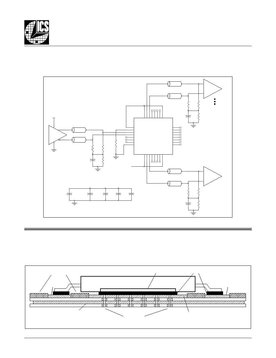
This application note provides general design guide using
ICS853111-02 LVPECL buffer.
Figure 6
shows a schematic ex-
ample of the ICS853111-02 LVPECL clock buffer. In this ex-
F
IGURE
6. E
XAMPLE
ICS853111-02 LVPECL C
LOCK
O
UTPUT
B
UFFER
S
CHEMATIC
ample, the input is driven by an LVPECL driver. CLK_SEL is set
at logic high to select PCLK0/nPCLK0 input.
C4
0.1uF
C6 (Option)
0.1u
Zo = 50
R7
50
Zo = 50
R2
50
VCC
R1
50
VCC
VCC=3.3V
C7 (Option)
0.1u
R3
50
(U1-16)
U1
ICS853111
1
2
3
4
5
6
7
8
9
10
11
12
13
14
15
16
17
18
19
20
21
22
23
24
32
31
30
29
28
27
26
25
VCC
CLK_SEL
PCLK0
nPCLK0
VBB
PCLK1
nPCLK1
VEE
VC
C
O
nQ
9
Q9
nQ
8
Q8
nQ
7
Q7
VC
C
O
nQ6
Q6
nQ5
Q5
nQ4
Q4
nQ3
Q3
VC
C
O
Q0
nQ
0
Q1
nQ
1
Q2
nQ
2
VC
C
O
R4
1K
Zo = 50
C2
0.1uF
(U1-9)
R8
50
Zo = 50 Ohm
C8 (Option)
0.1u
+
-
C5
0.1uF
R10
50
R11
50
3.3V LVPECL
+
-
VCC
(U1-32)
R13
50
C1
0.1uF
Zo = 50 Ohm
R9
50
C3
0.1uF
(U1-25)
VCC
Zo = 50
(U1-1)
EXPOSED PAD
Expose Metal Pad
(GROUND PAD)
GROUND PLANE
SOLDER
SIGNAL
TRACE
SIGNAL
TRACE
THERM AL VIA
SOLDER M ASK
F
IGURE
7. P.C. B
OARD
FOR
E
XPOSED
P
AD
T
HERMAL
R
ELEASE
P
ATH
E
XAMPLE
T
HERMAL
R
ELEASE
P
ATH
The expose metal pad provides heat transfer from the device to
the P.C. board. The expose metal pad is ground pad connected
to ground plane through thermal via. The exposed pad on the
device to the exposed metal pad on the PCB is contacted through
solder as shown in
Figure 7.
For further information, please re-
fer to the Application Note on Surface Mount Assembly of
Amkor's Thermally /Electrically Enhance Leadframe Base Pack-
age, Amkor Technology.

853111AY-02
www.icst.com/products/hiperclocks.html
REV. A JANUARY 10, 2006
13
Integrated
Circuit
Systems, Inc.
ICS853111-02
L
OW
S
KEW
, 1-
TO
-10
D
IFFERENTIAL
-
TO
-2.5V/3.3V LVPECL/ECL F
ANOUT
B
UFFER
P
OWER
C
ONSIDERATIONS
This section provides information on power dissipation and junction temperature for the ICS853111-02.
Equations and example calculations are also provided.
1. Power Dissipation.
The total power dissipation for the ICS853111-02 is the sum of the core power plus the power dissipated in the load(s).
The following is the power dissipation for V
CC
= 3.8V, which gives worst case results.
NOTE: Please refer to Section 3 for details on calculating power dissipated in the load.
�
Power (core)
MAX
= V
CC_MAX
* I
EE_MAX
= 3.8V * 85mA = 323mW
�
Power (outputs)
MAX
= 30.94mW/Loaded Output pair
If all outputs are loaded, the total power is 10 * 30.94mW = 309.4mW
Total Power
_MAX
(3.8V, with all outputs switching) = 323mW + 309.4mW = 632.4mW
2. Junction Temperature.
Junction temperature, Tj, is the temperature at the junction of the bond wire and bond pad and directly affects the reliability of the
device. The maximum recommended junction temperature for HiPerClockS
TM
devices is 125�C.
The equation for Tj is as follows: Tj =
JA
* Pd_total + T
A
Tj = Junction Temperature
JA
= Junction-to-Ambient Thermal Resistance
Pd_total = Total Device Power Dissipation (example calculation is in section 1 above)
T
A
= Ambient Temperature
In order to calculate junction temperature, the appropriate junction-to-ambient thermal resistance
JA
must be used. Assuming a
moderate air flow of 200 linear feet per minute and a multi-layer board, the appropriate value is 43.8�C/W per Table 6 below.
Therefore, Tj for an ambient temperature of 85�C with all outputs switching is:
85�C + 0.632W * 43.8�C/W = 112.7�C. This is below the limit of 125�C.
This calculation is only an example. Tj will obviously vary depending on the number of loaded outputs, supply voltage, air flow,
and the type of board (single layer or multi-layer).
JA
by Velocity (Linear Feet per Minute)
0
200
500
Single-Layer PCB, JEDEC Standard Test Boards
69.3�C/W
57.8�C/W
52.1�C/W
Multi-Layer PCB, JEDEC Standard Test Boards
49.5�C/W
43.8�C/W
41.3�C/W
NOTE: Most modern PCB designs use multi-layered boards. The data in the second row pertains to most designs.
T
ABLE
6. T
HERMAL
R
ESISTANCE
JA
FOR
32-
PIN
TQFP, E-PAD, F
ORCED
C
ONVECTION
853111AY-02
www.icst.com/products/hiperclocks.html
REV. A JANUARY 10, 2006
14
Integrated
Circuit
Systems, Inc.
ICS853111-02
L
OW
S
KEW
, 1-
TO
-10
D
IFFERENTIAL
-
TO
-2.5V/3.3V LVPECL/ECL F
ANOUT
B
UFFER
3. Calculations and Equations.
LVPECL output driver circuit and termination are shown in Figure 8.
T
o calculate worst case power dissipation into the load, use the following equations which assume a 50
load, and a termination
voltage of V
CCO
- 2V.
�
For logic high, V
OUT
= V
OH_MAX
= V
CCO_MAX
� 0.935V
(V
CC_MAX
- V
OH_MAX
) = 0.935V
�
For logic low, V
OUT
= V
OL_MAX
= V
CCO_MAX
� 1.67V
(V
CCO_MAX
- V
OL_MAX
) = 1.67V
Pd_H = [(V
OH_MAX
� (V
CCO_MAX
- 2V))/R
L
] * (V
CCO_MAX
- V
OH_MAX
) = [(2V - (V
CCO_MAX
- V
OH_MAX
))/R
L
] * (V
CCO _MAX
- V
OH_MAX
) =
[(2V - 0.935V)/50
] * 0.935V = 19.92mW
Pd_L = [(V
OL_MAX
� (V
CCO_MAX
- 2V))/R
L
] * (V
CCO_MAX
- V
OL_MAX
) = [(2V - (V
CCO_MAX
- V
OL_MAX
))/R
L
] * (V
CCO_MAX
- V
OL_MAX
) =
[(2V - 1.67V)/50
] * 1.67V = 11.02mW
Total Power Dissipation per output pair = Pd_H + Pd_L = 30.94mW
Figure 8. LVPECL Driver Circuit and Termination
VCCO - 2V
Q1
VOUT
RL
50
VCCO

853111AY-02
www.icst.com/products/hiperclocks.html
REV. A JANUARY 10, 2006
15
Integrated
Circuit
Systems, Inc.
ICS853111-02
L
OW
S
KEW
, 1-
TO
-10
D
IFFERENTIAL
-
TO
-2.5V/3.3V LVPECL/ECL F
ANOUT
B
UFFER
R
ELIABILITY
I
NFORMATION
T
RANSISTOR
C
OUNT
The transistor count for ICS853111-02 is: 1340
Pin compatible with MC100EP111 and MC100LVEP111
T
ABLE
7.
JA
VS
. A
IR
F
LOW
T
ABLE
FOR
32 L
EAD
TQFP, E-PAD
JA
by Velocity (Linear Feet per Minute)
0
200
500
Single-Layer PCB, JEDEC Standard Test Boards
69.3�C/W
57.8�C/W
52.1�C/W
Multi-Layer PCB, JEDEC Standard Test Boards
49.5�C/W
43.8�C/W
41.3�C/W
NOTE: Most modern PCB designs use multi-layered boards. The data in the second row pertains to most designs.
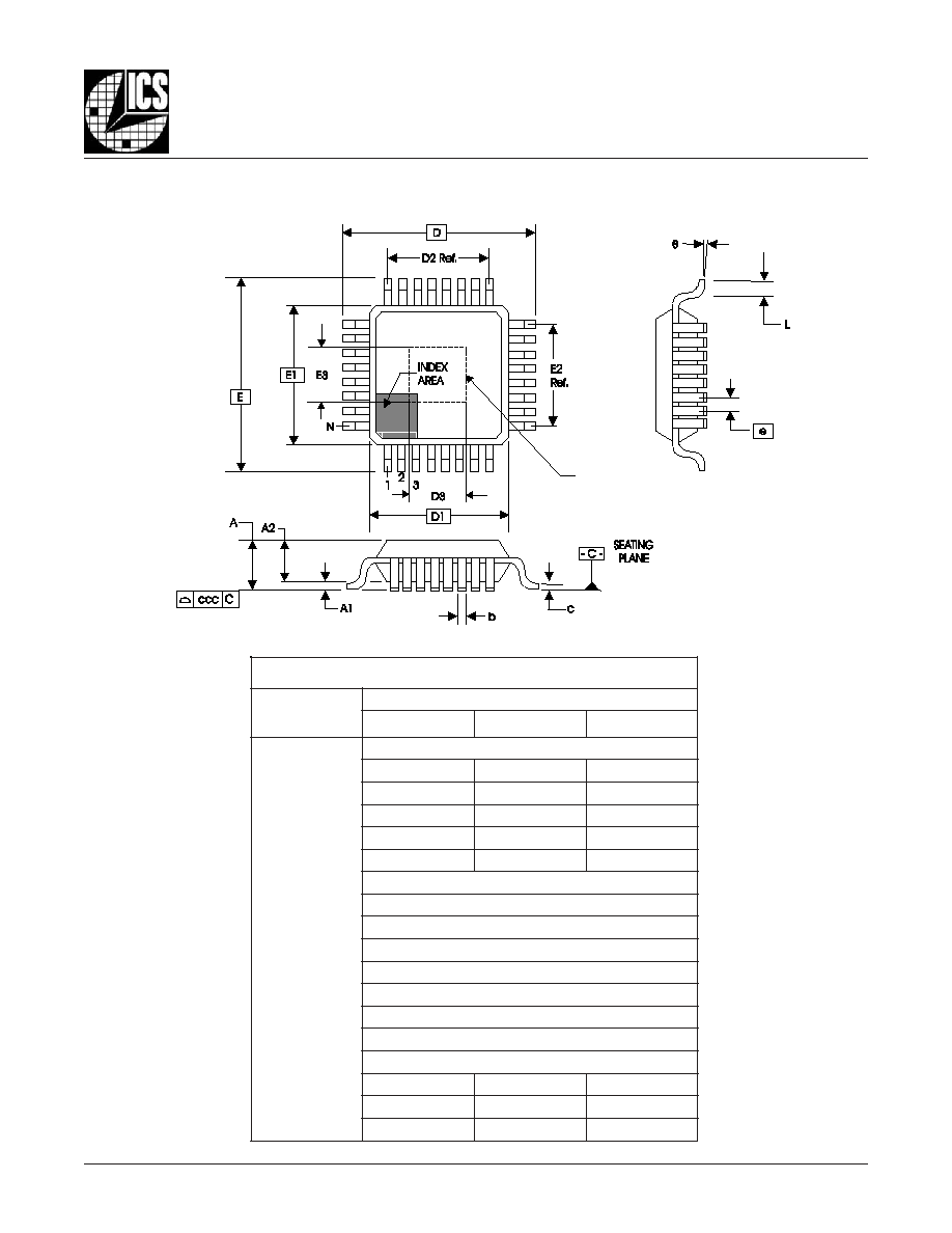
853111AY-02
www.icst.com/products/hiperclocks.html
REV. A JANUARY 10, 2006
16
Integrated
Circuit
Systems, Inc.
ICS853111-02
L
OW
S
KEW
, 1-
TO
-10
D
IFFERENTIAL
-
TO
-2.5V/3.3V LVPECL/ECL F
ANOUT
B
UFFER
Reference Document: JEDEC Publication 95, MS-026
TQFP P
ACKAGE
O
UTLINE
- Y S
UFFIX
FOR
32 L
EAD
TQFP, E-PAD
T
ABLE
8. P
ACKAGE
D
IMENSIONS
-HD VERSION
HEAT SLUG DOWN
N
O
I
T
A
I
R
A
V
C
E
D
E
J
S
R
E
T
E
M
I
L
L
I
M
N
I
S
N
O
I
S
N
E
M
I
D
L
L
A
L
O
B
M
Y
S
D
H
-
A
B
A
M
U
M
I
N
I
M
L
A
N
I
M
O
N
M
U
M
I
X
A
M
N
2
3
A
-
-
-
-
0
2
.
1
1
A
5
0
.
0
0
1
.
0
5
1
.
0
2
A
5
9
.
0
0
.
1
5
0
.
1
b
0
3
.
0
5
3
.
0
0
4
.
0
c
9
0
.
0
-
-
0
2
.
0
D
C
I
S
A
B
0
0
.
9
1
D
C
I
S
A
B
0
0
.
7
2
D
.
f
e
R
0
6
.
5
3
D
C
I
S
A
B
0
0
.
4
E
C
I
S
A
B
0
0
.
9
1
E
C
I
S
A
B
0
0
.
7
2
E
.
f
e
R
0
6
.
5
3
E
C
I
S
A
B
0
0
.
4
e
C
I
S
A
B
0
8
.
0
L
5
4
.
0
0
6
.
0
5
7
.
0
0
�
-
-
7
�
c
c
c
-
-
-
-
0
1
.
0
853111AY-02
www.icst.com/products/hiperclocks.html
REV. A JANUARY 10, 2006
17
Integrated
Circuit
Systems, Inc.
ICS853111-02
L
OW
S
KEW
, 1-
TO
-10
D
IFFERENTIAL
-
TO
-2.5V/3.3V LVPECL/ECL F
ANOUT
B
UFFER
T
ABLE
9. O
RDERING
I
NFORMATION
While the information presented herein has been checked for both accuracy and reliability, Integrated Circuit Systems, Incorporated (ICS) assumes no responsibility for either its use
or for infringement of any patents or other rights of third parties, which would result from its use. No other circuits, patents, or licenses are implied. This product is intended for use
in normal commercial and industrial applications. Any other applications such as those requiring high reliability or other extraordinary environmental requirements are not
recommended without additional processing by ICS. ICS reserves the right to change any circuitry or specifications without notice. ICS does not authorize or warrant any ICS product
for use in life support devices or critical medical instruments.
r
e
b
m
u
N
r
e
d
r
O
/
t
r
a
P
g
n
i
k
r
a
M
e
g
a
k
c
a
P
g
n
i
g
a
k
c
a
P
g
n
i
p
p
i
h
S
e
r
u
t
a
r
e
p
m
e
T
2
0
-
Y
A
1
1
1
3
5
8
S
C
I
2
0
A
1
1
1
3
5
8
S
C
I
P
F
Q
T
d
a
P
-
E
,
d
a
e
l
2
3
y
a
r
t
C
�
5
8
o
t
C
�
0
4
-
T
2
0
-
Y
A
1
1
1
3
5
8
S
C
I
2
0
A
1
1
1
3
5
8
S
C
I
P
F
Q
T
d
a
P
-
E
,
d
a
e
l
2
3
l
e
e
r
&
e
p
a
t
0
0
0
1
C
�
5
8
o
t
C
�
0
4
-
F
L
2
0
-
Y
A
1
1
1
3
5
8
S
C
I
L
2
0
A
1
1
1
3
5
8
S
C
I
P
F
Q
T
d
a
P
-
E
"
,
e
e
r
F
-
d
a
e
L
"
d
a
e
l
2
3
y
a
r
t
C
�
5
8
o
t
C
�
0
4
-
T
F
L
2
0
-
Y
A
1
1
1
3
5
8
S
C
I
L
2
0
A
1
1
1
3
5
8
S
C
I
P
F
Q
T
d
a
P
-
E
"
,
e
e
r
F
-
d
a
e
L
"
d
a
e
l
2
3
l
e
e
r
&
e
p
a
t
0
0
0
1
C
�
5
8
o
t
C
�
0
4
-
.
t
n
a
il
p
m
o
c
S
H
o
R
e
r
a
d
n
a
n
o
i
t
a
r
u
g
i
f
n
o
c
e
e
r
F
-
b
P
e
h
t
e
r
a
r
e
b
m
u
n
t
r
a
p
e
h
t
o
t
x
i
f
f
u
s
"
F
L
"
n
a
h
t
i
w
d
e
r
e
d
r
o
e
r
a
t
a
h
t
s
t
r
a
P
:
E
T
O
N
The aforementioned trademark, HiPerClockS is a trademark of Integrated Circuit Systems, Inc. or its subsidiaries in the United States and/or other countries.

853111AY-02
www.icst.com/products/hiperclocks.html
REV. A JANUARY 10, 2006
18
Integrated
Circuit
Systems, Inc.
ICS853111-02
L
OW
S
KEW
, 1-
TO
-10
D
IFFERENTIAL
-
TO
-2.5V/3.3V LVPECL/ECL F
ANOUT
B
UFFER
T
E
E
H
S
Y
R
O
T
S
I
H
N
O
I
S
I
V
E
R
v
e
R
e
l
b
a
T
e
g
a
P
e
g
n
a
h
C
f
o
n
o
i
t
p
i
r
c
s
e
D
e
t
a
D
A
9
T
0
1
7
1
d
e
d
d
A
.
s
n
i
P
t
u
p
t
u
O
d
n
a
t
u
p
n
I
d
e
s
u
n
U
r
o
f
s
n
o
i
t
a
d
n
e
m
m
o
c
e
R
.
g
n
i
k
r
a
m
e
e
r
F
-
d
a
e
L
d
e
d
d
a
-
e
l
b
a
T
n
o
i
t
a
m
r
o
f
n
I
g
n
i
r
e
d
r
O
6
0
/
0
1
/
1