Document Outline
- General Description
- Features
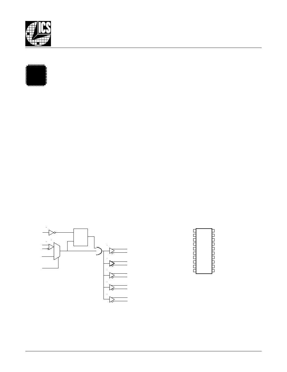
- Block Diagram
- Pin Assignment
- Pin Descriptions
- Pin Characteristics
- Control Input Function Table
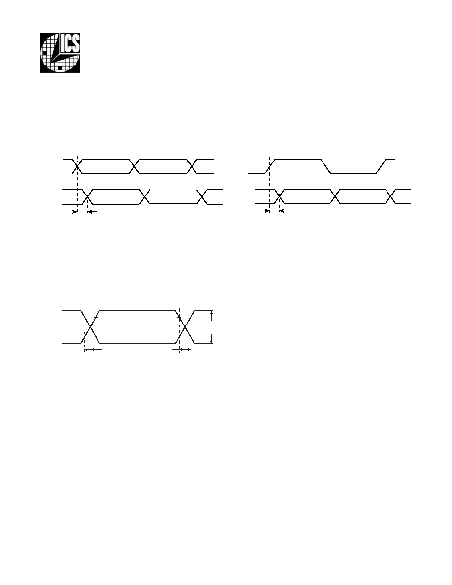
- nCLK_EN Timing Diagram
- Clock Input Function Table
- Absolute Maximum Ratings
- Power Supply DC Characteristics
- LVCMOS DC Characteristics
- Differential DC Characteristics
- LVPECL DC Characteristics
- AC Characteristics
- Typical Phase Noise Plot at 155.52MHz
- Parameter Measurement Information
- Parameter Measurement Information, continued
- Application Information
- Wiring the Differential Input to Accept Single Ended Levels
- Recommendations for Unused Input and Output Pins
- Differential Clock Input Interface
- Termination for 3.3V LVPECL Outputs
- Termination for 2.5V LVPECL Outputs
- Power Considerations
- Power Dissipation
- Junction Temperature
- Thermal Resistance, 20 pin TSSOP
- Thermal Resistance, 20 pin SOIC
- Calculations & Equations
- LVPECL Driver Circuit & Termination Diagram
- Reliability Information
- Transistor Count
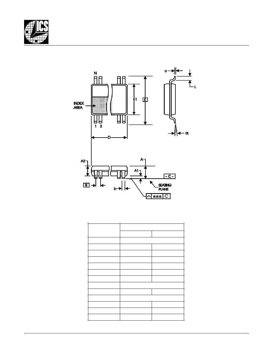
- Package Outline, TSSOP
- Package Dimensions, TSSOP
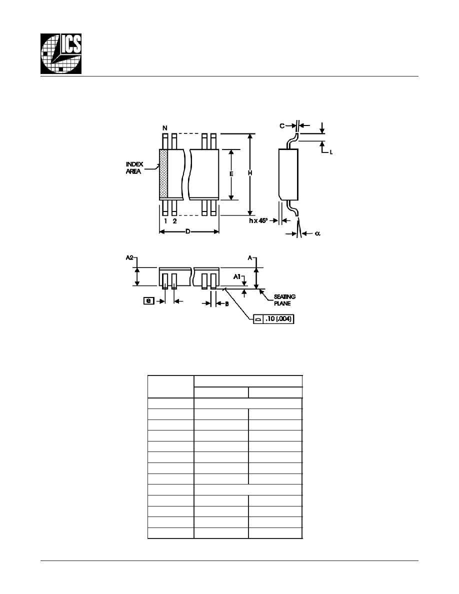
- Package Outline, SOIC
- Package Dimensions, SOIC
- Ordering Information
- Revision History Sheet
85314BGI-01
www.icst.com/products/hiperclocks.html
REV. E SEPTEMBER 23, 2005
1
Integrated
Circuit
Systems, Inc.
ICS85314I-01
L
OW
S
KEW
, 1-
TO
-5
D
IFFERENTIAL
-
TO
-2.5V/3.3V LVPECL F
ANOUT
B
UFFER
G
ENERAL
D
ESCRIPTION
The ICS85314I-01 is a low skew, high perfor-
mance 1-to-5 Differential-to-2.5V/3.3V LVPECL
Fanout Buffer and a member of the HiPerClockSTM
family of High Performance Clock Solutions from
ICS. The ICS85314I-01 has two selectable clock
inputs. The CLK0, nCLK0 pair can accept most standard
differential input levels. The single-ended CLK1 can accept
LVCMOS or LVTTL input levels. The clock enable is internally
synchronized to eliminate runt clock pulses on the outputs
during asynchronous assertion/deassertion of the clock
enable pin.
Guaranteed output and part-to-part skew characteristics
make the ICS85314I-01 ideal for those applications demand-
ing well defined performance and repeatability.
F
EATURES
� 5 differential 2.5V/3.3V LVPECL outputs
� Selectable differential CLK0, nCLK0 or LVCMOS inputs
� CLK0, nCLK0 pair can accept the following differential
input levels: LVPECL, LVDS, LVHSTL, HCSL, SSTL
� CLK1 can accept the following input levels:
LVCMOS or LVTTL
� Maximum output frequency: 700MHz
� Translates any single-ended input signal to 3.3V
LVPECL levels with resistor bias on nCLK input
� Output skew: 30ps (maximum), TSSOP package
50ps (maximum), SOIC package
� Part-to-part skew: 350ps (maximum)
� Propagation delay: 1.8ns (maximum)
� RMS phase jitter @ 155.52MHz (12kHz - 20MHz):
0.05ps (typical)
� LVPECL mode operating voltage supply range:
V
CC
= 2.375V to 3.8V, V
EE
= 0V
� -40�C to 85�C ambient operating temperature
� Available in both standard and lead-free RoHS-compliant
packages
B
LOCK
D
IAGRAM
P
IN
A
SSIGNMENT
Q0
nQ0
Q1
nQ1
Q2
nQ2
Q3
nQ3
Q4
nQ4
1
2
3
4
5
6
7
8
9
10
20
19
18
17
16
15
14
13
12
11
V
CC
nCLK_EN
V
CC
nc
CLK1
CLK0
nCLK0
nc
CLK_SEL
V
EE
HiPerClockSTM
ICS
ICS85314I-01
20-Lead TSSOP
6.5mm x 4.4mm x 0.92mm Package Body
G Package
Top View
ICS85314I-01
20-Lead SOIC
7.5mm x 12.8mm x 2.3mm Package Body
M Package
Top View
CLK0
nCLK0
CLK1
Q0
nQ0
Q1
nQ1
Q2
nQ2
Q3
nQ3
Q4
nQ4
0
1
nCLK_EN
CLK_SEL
D
Q
LE
0
1

85314BGI-01
www.icst.com/products/hiperclocks.html
REV. E SEPTEMBER 23, 2005
2
Integrated
Circuit
Systems, Inc.
ICS85314I-01
L
OW
S
KEW
, 1-
TO
-5
D
IFFERENTIAL
-
TO
-2.5V/3.3V LVPECL F
ANOUT
B
UFFER
T
ABLE
1. P
IN
D
ESCRIPTIONS
T
ABLE
2. P
IN
C
HARACTERISTICS
l
o
b
m
y
S
r
e
t
e
m
a
r
a
P
s
n
o
i
t
i
d
n
o
C
t
s
e
T
m
u
m
i
n
i
M
l
a
c
i
p
y
T
m
u
m
i
x
a
M
s
t
i
n
U
C
N
I
e
c
n
a
t
i
c
a
p
a
C
t
u
p
n
I
4
F
p
R
P
U
L
L
U
P
r
o
t
s
i
s
e
R
p
u
ll
u
P
t
u
p
n
I
1
5
k
R
N
W
O
D
L
L
U
P
r
o
t
s
i
s
e
R
n
w
o
d
ll
u
P
t
u
p
n
I
1
5
k
r
e
b
m
u
N
e
m
a
N
e
p
y
T
n
o
i
t
p
i
r
c
s
e
D
2
,
1
0
Q
n
,
0
Q
t
u
p
t
u
O
.
s
l
e
v
e
l
e
c
a
f
r
e
t
n
i
L
C
E
P
V
L
.
r
i
a
p
t
u
p
t
u
o
l
a
i
t
n
e
r
e
f
f
i
D
4
,
3
1
Q
n
,
1
Q
t
u
p
t
u
O
.
s
l
e
v
e
l
e
c
a
f
r
e
t
n
i
L
C
E
P
V
L
.
r
i
a
p
t
u
p
t
u
o
l
a
i
t
n
e
r
e
f
f
i
D
6
,
5
2
Q
n
,
2
Q
t
u
p
t
u
O
.
s
l
e
v
e
l
e
c
a
f
r
e
t
n
i
L
C
E
P
V
L
.
r
i
a
p
t
u
p
t
u
o
l
a
i
t
n
e
r
e
f
f
i
D
8
,
7
3
Q
n
,
3
Q
t
u
p
t
u
O
.
s
l
e
v
e
l
e
c
a
f
r
e
t
n
i
L
C
E
P
V
L
.
r
i
a
p
t
u
p
t
u
o
l
a
i
t
n
e
r
e
f
f
i
D
0
1
,
9
4
Q
n
,
4
Q
t
u
p
t
u
O
.
s
l
e
v
e
l
e
c
a
f
r
e
t
n
i
L
C
E
P
V
L
.
r
i
a
p
t
u
p
t
u
o
l
a
i
t
n
e
r
e
f
f
i
D
1
1
V
E
E
r
e
w
o
P
.
n
i
p
y
l
p
p
u
s
e
v
i
t
a
g
e
N
2
1
L
E
S
_
K
L
C
t
u
p
n
I
n
w
o
d
ll
u
P
.
t
u
p
n
i
1
K
L
C
s
t
c
e
l
e
s
,
H
G
I
H
n
e
h
W
.
t
u
p
n
i
t
c
e
l
e
s
k
c
o
l
C
.
s
t
u
p
n
i
0
K
L
C
n
,
0
K
L
C
s
t
c
e
l
e
s
,
W
O
L
n
e
h
W
.
s
l
e
v
e
l
e
c
a
f
r
e
t
n
i
S
O
M
C
V
L
/
L
T
T
V
L
7
1
,
3
1
c
n
d
e
s
u
n
U
.
t
c
e
n
n
o
c
o
N
4
1
0
K
L
C
n
t
u
p
n
I
p
u
ll
u
P
.
t
u
p
n
i
k
c
o
l
c
l
a
i
t
n
e
r
e
f
f
i
d
g
n
i
t
r
e
v
n
I
5
1
0
K
L
C
t
u
p
n
I
n
w
o
d
ll
u
P
.
t
u
p
n
i
k
c
o
l
c
l
a
i
t
n
e
r
e
f
f
i
d
g
n
i
t
r
e
v
n
i
-
n
o
N
6
1
1
K
L
C
t
u
p
n
I
n
w
o
d
ll
u
P
.
s
l
e
v
e
l
e
c
a
f
r
e
t
n
i
S
O
M
C
V
L
/
L
T
T
V
L
.
t
u
p
n
i
k
c
o
l
C
0
2
,
8
1
V
C
C
r
e
w
o
P
.
s
n
i
p
y
l
p
p
u
s
e
v
i
t
i
s
o
P
9
1
N
E
_
K
L
C
n
t
u
p
n
I
n
w
o
d
ll
u
P
k
c
o
l
c
w
o
ll
o
f
s
t
u
p
t
u
o
k
c
o
l
c
,
W
O
L
n
e
h
W
.
e
l
b
a
n
e
k
c
o
l
c
g
n
i
z
i
n
o
r
h
c
n
y
S
d
e
c
r
o
f
e
r
a
s
t
u
p
t
u
o
Q
n
,
w
o
l
d
e
c
r
o
f
e
r
a
s
t
u
p
t
u
o
Q
,
H
G
I
H
n
e
h
W
.
t
u
p
n
i
.
s
l
e
v
e
l
e
c
a
f
r
e
t
n
i
S
O
M
C
V
L
/
L
T
T
V
L
.
h
g
i
h
:
E
T
O
N
p
u
ll
u
P
d
n
a
n
w
o
d
ll
u
P
.
s
e
u
l
a
v
l
a
c
i
p
y
t
r
o
f
,
s
c
i
t
s
i
r
e
t
c
a
r
a
h
C
n
i
P
,
2
e
l
b
a
T
e
e
S
.
s
r
o
t
s
i
s
e
r
t
u
p
n
i
l
a
n
r
e
t
n
i
o
t
r
e
f
e
r

85314BGI-01
www.icst.com/products/hiperclocks.html
REV. E SEPTEMBER 23, 2005
3
Integrated
Circuit
Systems, Inc.
ICS85314I-01
L
OW
S
KEW
, 1-
TO
-5
D
IFFERENTIAL
-
TO
-2.5V/3.3V LVPECL F
ANOUT
B
UFFER
T
ABLE
3A. C
ONTROL
I
NPUT
F
UNCTION
T
ABLE
T
ABLE
3B. C
LOCK
I
NPUT
F
UNCTION
T
ABLE
s
t
u
p
n
I
s
t
u
p
t
u
O
N
E
_
K
L
C
n
L
E
S
_
K
L
C
e
c
r
u
o
S
d
e
t
c
e
l
e
S
4
Q
:
0
Q
4
Q
n
:
0
Q
n
0
0
0
K
L
C
n
,
0
K
L
C
d
e
l
b
a
n
E
d
e
l
b
a
n
E
0
1
1
K
L
C
d
e
l
b
a
n
E
d
e
l
b
a
n
E
1
0
0
K
L
C
n
,
0
K
L
C
W
O
L
;
d
e
l
b
a
s
i
D
H
G
I
H
;
d
e
l
b
a
s
i
D
1
1
1
K
L
C
W
O
L
;
d
e
l
b
a
s
i
D
H
G
I
H
;
d
e
l
b
a
s
i
D
e
g
d
e
k
c
o
l
c
t
u
p
n
i
g
n
il
l
a
f
a
g
n
i
w
o
ll
o
f
d
e
l
b
a
n
e
r
o
d
e
l
b
a
s
i
d
e
r
a
s
t
u
p
t
u
o
k
c
o
l
c
e
h
t
,
s
e
h
c
t
i
w
s
N
E
_
K
L
C
n
r
e
t
f
A
.
1
e
r
u
g
i
F
n
i
n
w
o
h
s
s
a
s
t
u
p
n
i
1
K
L
C
d
n
a
0
K
L
C
n
,
0
K
L
C
e
h
t
f
o
n
o
i
t
c
n
u
f
a
e
r
a
s
t
u
p
t
u
o
e
h
t
f
o
e
t
a
t
s
e
h
t
,
e
d
o
m
e
v
i
t
c
a
e
h
t
n
I
.
B
3
e
l
b
a
T
n
i
d
e
b
i
r
c
s
e
d
s
a
s
t
u
p
n
I
s
t
u
p
t
u
O
e
d
o
M
t
u
p
t
u
O
o
t
t
u
p
n
I
y
t
i
r
a
l
o
P
1
K
L
C
r
o
0
K
L
C
0
K
L
C
n
4
Q
:
0
Q
4
Q
n
:
0
Q
n
0
1
W
O
L
H
G
I
H
l
a
i
t
n
e
r
e
f
f
i
D
o
t
l
a
i
t
n
e
r
e
f
f
i
D
g
n
i
t
r
e
v
n
I
n
o
N
1
0
H
G
I
H
W
O
L
l
a
i
t
n
e
r
e
f
f
i
D
o
t
l
a
i
t
n
e
r
e
f
f
i
D
g
n
i
t
r
e
v
n
I
n
o
N
F
IGURE
1. nCLK_EN T
IMING
D
IAGRAM
Enabled
Disabled
nCLK0
CLK0, CLK1
nCLK_EN
nQ0:nQ4
Q0:Q4

85314BGI-01
www.icst.com/products/hiperclocks.html
REV. E SEPTEMBER 23, 2005
4
Integrated
Circuit
Systems, Inc.
ICS85314I-01
L
OW
S
KEW
, 1-
TO
-5
D
IFFERENTIAL
-
TO
-2.5V/3.3V LVPECL F
ANOUT
B
UFFER
T
ABLE
4A. P
OWER
S
UPPLY
DC C
HARACTERISTICS
,
V
CC
= 2.375V
TO
3.8V, V
EE
= 0V, T
A
= -40�C
TO
85�C
T
ABLE
4B. LVCMOS / LVTTL DC C
HARACTERISTICS
,
V
CC
= 2.375V
TO
3.8V, V
EE
= 0V, T
A
= -40�C
TO
85�C
l
o
b
m
y
S
r
e
t
e
m
a
r
a
P
s
n
o
i
t
i
d
n
o
C
t
s
e
T
m
u
m
i
n
i
M
l
a
c
i
p
y
T
m
u
m
i
x
a
M
s
t
i
n
U
V
H
I
e
g
a
t
l
o
V
h
g
i
H
t
u
p
n
I
L
E
S
_
K
L
C
,
N
E
_
K
L
C
n
2
V
C
C
3
.
0
+
V
1
K
L
C
2
V
C
C
3
.
0
+
V
V
L
I
e
g
a
t
l
o
V
w
o
L
t
u
p
n
I
L
E
S
_
K
L
C
,
N
E
_
K
L
C
n
3
.
0
-
8
.
0
V
1
K
L
C
3
.
0
-
3
.
1
V
I
H
I
t
n
e
r
r
u
C
h
g
i
H
t
u
p
n
I
,
1
K
L
C
N
E
_
K
L
C
n
,
L
E
S
_
K
L
C
V
N
I
V
=
C
C
V
8
.
3
=
0
5
1
A
�
I
L
I
t
n
e
r
r
u
C
w
o
L
t
u
p
n
I
,
1
K
L
C
N
E
_
K
L
C
n
,
L
E
S
_
K
L
C
V
C
C
V
,
V
8
.
3
=
N
I
V
0
=
5
-
A
�
l
o
b
m
y
S
r
e
t
e
m
a
r
a
P
s
n
o
i
t
i
d
n
o
C
t
s
e
T
m
u
m
i
n
i
M
l
a
c
i
p
y
T
m
u
m
i
x
a
M
s
t
i
n
U
V
C
C
e
g
a
t
l
o
V
y
l
p
p
u
S
r
e
w
o
P
5
7
3
.
2
3
.
3
8
.
3
V
I
E
E
t
n
e
r
r
u
C
y
l
p
p
u
S
r
e
w
o
P
0
8
A
m
T
ABLE
4C. D
IFFERENTIAL
DC C
HARACTERISTICS
,
V
CC
= 2.375V
TO
3.8V, V
EE
= 0V, T
A
= -40�C
TO
85�C
l
o
b
m
y
S
r
e
t
e
m
a
r
a
P
s
n
o
i
t
i
d
n
o
C
t
s
e
T
m
u
m
i
n
i
M
l
a
c
i
p
y
T
m
u
m
i
x
a
M
s
t
i
n
U
I
H
I
t
n
e
r
r
u
C
h
g
i
H
t
u
p
n
I
0
K
L
C
n
V
C
C
V
=
N
I
V
8
.
3
=
5
A
�
0
K
L
C
V
C
C
V
=
N
I
V
8
.
3
=
0
5
1
A
�
I
L
I
t
n
e
r
r
u
C
w
o
L
t
u
p
n
I
0
K
L
C
n
V
C
C
V
,
V
8
.
3
=
N
I
V
0
=
0
5
1
-
A
�
0
K
L
C
V
C
C
V
,
V
8
.
3
=
N
I
V
0
=
5
-
A
�
V
P
P
e
g
a
t
l
o
V
t
u
p
n
I
k
a
e
P
-
o
t
-
k
a
e
P
5
1
.
0
3
.
1
V
V
R
M
C
;
e
g
a
t
l
o
V
t
u
p
n
I
e
d
o
M
n
o
m
m
o
C
2
,
1
E
T
O
N
5
.
0
V
C
C
5
8
.
0
-
V
V
s
i
0
K
L
C
n
,
0
K
L
C
r
o
f
e
g
a
t
l
o
v
t
u
p
n
i
m
u
m
i
x
a
m
e
h
t
s
n
o
i
t
a
c
il
p
p
a
d
e
d
n
e
e
l
g
n
i
s
r
o
F
:
1
E
T
O
N
C
C
.
V
3
.
0
+
V
s
a
d
e
n
i
f
e
d
s
i
e
g
a
t
l
o
v
e
d
o
m
n
o
m
m
o
C
:
2
E
T
O
N
H
I
.
A
BSOLUTE
M
AXIMUM
R
ATINGS
Supply Voltage, V
CC
4.6V
Inputs, V
I
-0.5V to V
CC
+ 0.5V
Outputs, I
O
Continuous Current
50mA
Surge Current
100mA
Package Thermal Impedance,
JA
20 Lead TSSOP
73.2�C/W (0 lfpm)
20 Lead SOIC
46.2�C/W (0 lfpm)
Storage Temperature, T
STG
-65�C to 150�C
NOTE: Stresses beyond those listed under Absolute
Maximum Ratings may cause permanent damage to the
device. These ratings are stress specifications only. Functional
operation of product at these conditions or any conditions be-
yond those listed in the
DC Characteristics
or
AC Character-
istics
is not implied. Exposure to absolute maximum rating
conditions for extended periods may affect product reliability.
85314BGI-01
www.icst.com/products/hiperclocks.html
REV. E SEPTEMBER 23, 2005
5
Integrated
Circuit
Systems, Inc.
ICS85314I-01
L
OW
S
KEW
, 1-
TO
-5
D
IFFERENTIAL
-
TO
-2.5V/3.3V LVPECL F
ANOUT
B
UFFER
T
ABLE
4D. LVPECL DC C
HARACTERISTICS
,
V
CC
= 2.375V
TO
3.8V, V
EE
= 0V, T
A
= -40�C
TO
85�C
T
ABLE
5. AC C
HARACTERISTICS
,
V
CC
= 2.375V
TO
3.8V, V
EE
= 0V, T
A
= -40�C
TO
85�C
l
o
b
m
y
S
r
e
t
e
m
a
r
a
P
s
n
o
i
t
i
d
n
o
C
t
s
e
T
m
u
m
i
n
i
M
l
a
c
i
p
y
T
m
u
m
i
x
a
M
s
t
i
n
U
f
X
A
M
y
c
n
e
u
q
e
r
F
t
u
p
t
u
O
0
K
L
C
n
,
0
K
L
C
0
0
7
z
H
M
1
K
L
C
0
0
3
z
H
M
)
�
(
t
ij
t
5
E
T
O
N
;
)
m
o
d
n
a
R
(
r
e
t
t
i
J
e
s
a
h
P
S
M
R
:
e
g
n
a
R
n
o
i
t
a
r
g
e
t
n
I
)
z
H
M
0
2
-
z
H
k
2
1
(
5
0
.
0
s
p
p
t
H
L
1
E
T
O
N
;
h
g
i
H
o
t
w
o
L
,
y
a
l
e
D
n
o
i
t
a
g
a
p
o
r
P
0
.
1
4
.
1
8
.
1
s
n
t
)
o
(
k
s
;
w
e
k
S
t
u
p
t
u
O
6
,
3
E
T
O
N
e
g
a
k
c
a
P
P
O
S
S
T
0
3
s
p
e
g
a
k
c
a
P
C
I
O
S
0
5
s
p
t
)
p
p
(
k
s
6
,
4
E
T
O
N
;
w
e
k
S
t
r
a
P
-
o
t
-
t
r
a
P
0
5
3
s
p
t
R
t
/
F
e
m
i
T
ll
a
F
/
e
s
i
R
t
u
p
t
u
O
%
0
8
o
t
%
0
2
0
0
2
0
0
7
s
p
c
d
o
e
l
c
y
C
y
t
u
D
t
u
p
t
u
O
0
K
L
C
n
,
0
K
L
C
z
H
M
0
0
7
5
4
5
5
%
1
K
L
C
z
H
M
0
5
2
5
4
5
5
%
f
t
a
d
e
r
u
s
a
e
m
s
r
e
t
e
m
a
r
a
p
ll
A
X
A
M
.
e
s
i
w
r
e
h
t
o
d
e
t
o
n
s
s
e
l
n
u
r
e
t
t
ij
d
d
a
t
o
n
s
e
o
d
t
r
a
p
e
h
T
.
t
u
p
t
u
o
e
h
t
n
o
r
e
t
t
ij
e
h
t
l
a
u
q
e
ll
i
w
t
u
p
n
i
e
h
t
n
o
r
e
t
t
ij
e
l
c
y
c
-
o
t
-
e
l
c
y
c
e
h
T
.
t
n
i
o
p
g
n
i
s
s
o
r
c
t
u
p
t
u
o
l
a
i
t
n
e
r
e
f
f
i
d
e
h
t
o
t
t
n
i
o
p
g
n
i
s
s
o
r
c
t
u
p
n
i
l
a
i
t
n
e
r
e
f
f
i
d
e
h
t
m
o
r
f
d
e
r
u
s
a
e
M
:
1
E
T
O
N
V
m
o
r
f
d
e
r
u
s
a
e
M
:
2
E
T
O
N
C
C
.
t
n
i
o
p
g
n
i
s
s
o
r
c
t
u
p
t
u
o
l
a
i
t
n
e
r
e
f
f
i
d
e
h
t
o
t
t
n
i
o
p
g
n
i
s
s
o
r
c
t
u
p
n
i
2
/
.
s
n
o
i
t
i
d
n
o
c
d
a
o
l
l
a
u
q
e
h
t
i
w
d
n
a
e
g
a
t
l
o
v
y
l
p
p
u
s
e
m
a
s
e
h
t
t
a
s
t
u
p
t
u
o
n
e
e
w
t
e
b
w
e
k
s
s
a
d
e
n
i
f
e
D
:
3
E
T
O
N
.
s
t
n
i
o
p
s
s
o
r
c
l
a
i
t
n
e
r
e
f
f
i
d
t
u
p
t
u
o
e
h
t
t
a
d
e
r
u
s
a
e
M
s
e
g
a
t
l
o
v
y
l
p
p
u
s
e
m
a
s
e
h
t
t
a
g
n
i
t
a
r
e
p
o
s
e
c
i
v
e
d
t
n
e
r
e
f
f
i
d
n
o
s
t
u
p
t
u
o
n
e
e
w
t
e
b
w
e
k
s
s
a
d
e
n
i
f
e
D
:
4
E
T
O
N
d
e
r
u
s
a
e
m
e
r
a
s
t
u
p
t
u
o
e
h
t
,
e
c
i
v
e
d
h
c
a
e
n
o
s
t
u
p
n
i
f
o
e
p
y
t
e
m
a
s
e
h
t
g
n
i
s
U
.
s
n
o
i
t
i
d
n
o
c
d
a
o
l
l
a
u
q
e
h
t
i
w
d
n
a
.
s
t
n
i
o
p
s
s
o
r
c
l
a
i
t
n
e
r
e
f
f
i
d
e
h
t
t
a
.
t
o
l
P
e
s
i
o
N
e
s
a
h
P
e
h
t
o
t
r
e
f
e
r
e
s
a
e
l
P
:
5
E
T
O
N
.
5
6
d
r
a
d
n
a
t
S
C
E
D
E
J
h
t
i
w
e
c
n
a
d
r
o
c
c
a
n
i
d
e
n
i
f
e
d
s
i
r
e
t
e
m
a
r
a
p
s
i
h
T
:
6
E
T
O
N
l
o
b
m
y
S
r
e
t
e
m
a
r
a
P
s
n
o
i
t
i
d
n
o
C
t
s
e
T
m
u
m
i
n
i
M
l
a
c
i
p
y
T
m
u
m
i
x
a
M
s
t
i
n
U
V
H
O
1
E
T
O
N
;
e
g
a
t
l
o
V
h
g
i
H
t
u
p
t
u
O
V
C
C
4
.
1
-
V
C
C
9
.
0
-
V
V
L
O
1
E
T
O
N
;
e
g
a
t
l
o
V
w
o
L
t
u
p
t
u
O
V
C
C
0
.
2
-
V
C
C
7
.
1
-
V
V
G
N
I
W
S
g
n
i
w
S
e
g
a
t
l
o
V
t
u
p
t
u
O
k
a
e
P
-
o
t
-
k
a
e
P
6
.
0
0
.
1
V
0
5
h
t
i
w
d
e
t
a
n
i
m
r
e
t
s
t
u
p
t
u
O
:
1
E
T
O
N
V
o
t
C
C
.
V
2
-
85314BGI-01
www.icst.com/products/hiperclocks.html
REV. E SEPTEMBER 23, 2005
6
Integrated
Circuit
Systems, Inc.
ICS85314I-01
L
OW
S
KEW
, 1-
TO
-5
D
IFFERENTIAL
-
TO
-2.5V/3.3V LVPECL F
ANOUT
B
UFFER
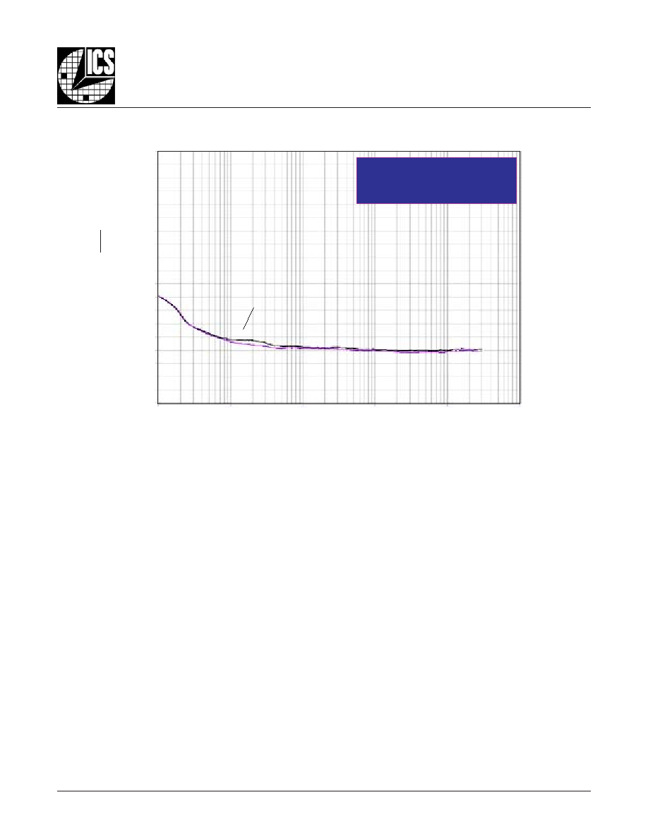
T
YPICAL
P
HASE
N
OISE
AT
155.52MH
Z
0
-10
-20
-30
-40
-50
-60
-70
-80
-90
-100
-110
-120
-130
-140
-150
-160
-170
-180
-190
1k
10k
100k
1M
10M
100M
155.52MHz
RMS Phase Jitter (Random)
12kHz to 20MHz = 0.05ps (typical)
O
FFSET
F
REQUENCY
(H
Z
)
N
OISE
P
O
WER
dBc
Hz
Raw Phase Noise Data
85314BGI-01
www.icst.com/products/hiperclocks.html
REV. E SEPTEMBER 23, 2005
7
Integrated
Circuit
Systems, Inc.
ICS85314I-01
L
OW
S
KEW
, 1-
TO
-5
D
IFFERENTIAL
-
TO
-2.5V/3.3V LVPECL F
ANOUT
B
UFFER
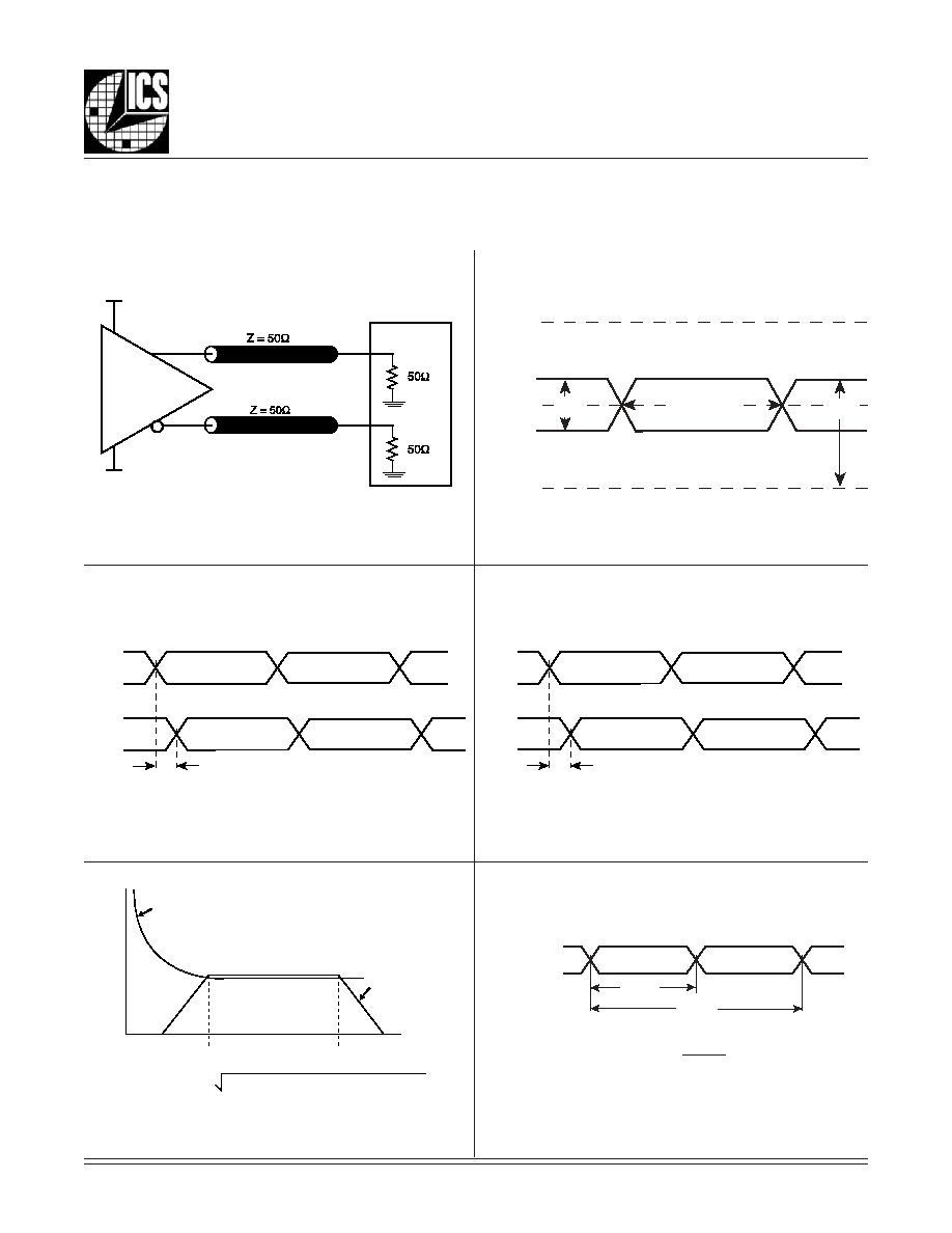
P
ARAMETER
M
EASUREMENT
I
NFORMATION
D
IFFERENTIAL
I
NPUT
L
EVEL
3.3V O
UTPUT
L
OAD
AC T
EST
C
IRCUIT
SCOPE
Qx
nQx
LVPECL
2V
-1.8V � -0.375V
V
CMR
Cross Points
V
PP
V
CC
V
EE
CLK0
nCLK0
V
CC
V
EE
P
ART
-
TO
-P
ART
S
KEW
t
sk(o)
nQx
Qx
nQy
Qy
O
UTPUT
S
KEW
RMS P
HASE
J
ITTER
Phase Noise Mask
Offset Frequency
f
1
f
2
Phase Noise Plot
RMS Jitter = Area Under the Masked Phase Noise Plot
Noise P
o
w
er
O
UTPUT
D
UTY
C
YCLE
/P
ULSE
W
IDTH
/P
ERIOD
t
PW
t
PERIOD
t
PW
t
PERIOD
odc =
x 100%
Q0:Q4
nQ0:nQ4
t
sk(o)
Qx
Qy
PART 1
PART 2
nQx
nQy
85314BGI-01
www.icst.com/products/hiperclocks.html
REV. E SEPTEMBER 23, 2005
8
Integrated
Circuit
Systems, Inc.
ICS85314I-01
L
OW
S
KEW
, 1-
TO
-5
D
IFFERENTIAL
-
TO
-2.5V/3.3V LVPECL F
ANOUT
B
UFFER
t
PD
P
ROPAGATION
D
ELAY
(D
IFFERENTIAL
I
NPUT
)
O
UTPUT
R
ISE
/F
ALL
T
IME
Clock
Outputs
20%
80%
80%
20%
t
R
t
F
V
SW I N G
CLK0
nCLK0
Q0:Q4
nQ0:nQ4
P
ROPAGATION
D
ELAY
(LVCMOS I
NPUT
)
t
PD
CLK1
Q0:Q4
nQ0:nQ4
85314BGI-01
www.icst.com/products/hiperclocks.html
REV. E SEPTEMBER 23, 2005
9
Integrated
Circuit
Systems, Inc.
ICS85314I-01
L
OW
S
KEW
, 1-
TO
-5
D
IFFERENTIAL
-
TO
-2.5V/3.3V LVPECL F
ANOUT
B
UFFER
A
PPLICATION
I
NFORMATION
F
IGURE
2. S
INGLE
E
NDED
S
IGNAL
D
RIVING
D
IFFERENTIAL
I
NPUT
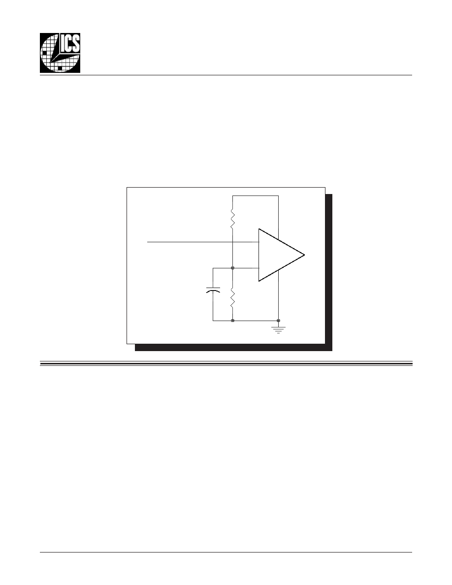
Figure 2
shows how the differential input can be wired to accept
single ended levels. The reference voltage V_REF = V
CC
/2 is
generated by the bias resistors R1, R2 and C1. This bias circuit
should be located as close as possible to the input pin. The ratio
W
IRING
THE
D
IFFERENTIAL
I
NPUT
TO
A
CCEPT
S
INGLE
E
NDED
L
EVELS
of R1 and R2 might need to be adjusted to position the V_REF in
the center of the input voltage swing. For example, if the input
clock swing is only 2.5V and V
CC
= 3.3V, V_REF should be 1.25V
and R2/R1 = 0.609.
V_REF
R1
1K
C1
0.1u
R2
1K
Single Ended Clock Input
CLK
nCLK
VCC
I
NPUTS
:
CLK I
NPUT
:
For applications not requiring the use of a clock input, it can
be left floating. Though not required, but for additional
protection, a 1k
resistor can be tied from the CLK input to
ground.
CLK/nCLK I
NPUT
:
For applications not requiring the use of the differential input,
both CLK and nCLK can be left floating. Though not required,
but for additional protection, a 1k
resistor can be tied from
CLK to ground.
LVCMOS C
ONTROL
P
INS
:
All control pins have internal pull-ups or pull-downs; additional
resistance is not required but can be added for additional
protection. A 1k
resistor can be used.
R
ECOMMENDATIONS
FOR
U
NUSED
I
NPUT
AND
O
UTPUT
P
INS
O
UTPUTS
:
LVPECL O
UTPUT
All unused LVPECL outputs can be left floating. We
recommend that there is no trace attached. Both sides of the
differential output pair should either be left floating or
terminated.
85314BGI-01
www.icst.com/products/hiperclocks.html
REV. E SEPTEMBER 23, 2005
10
Integrated
Circuit
Systems, Inc.
ICS85314I-01
L
OW
S
KEW
, 1-
TO
-5
D
IFFERENTIAL
-
TO
-2.5V/3.3V LVPECL F
ANOUT
B
UFFER
F
IGURE
3C. H
I
P
ER
C
LOCK
S CLK/
N
CLK I
NPUT
D
RIVEN
BY
3.3V LVPECL D
RIVER
F
IGURE
3B. H
I
P
ER
C
LOCK
S CLK/
N
CLK I
NPUT
D
RIVEN
BY
3.3V LVPECL D
RIVER
F
IGURE
3D. H
I
P
ER
C
LOCK
S CLK/
N
CLK I
NPUT
D
RIVEN
BY
3.3V LVDS D
RIVER
3.3V
R1
50
R3
50
Zo = 50 Ohm
LVPECL
Zo = 50 Ohm
HiPerClockS
CLK
nCLK
3.3V
Input
R2
50
Zo = 50 Ohm
Input
HiPerClockS
CLK
nCLK
3.3V
R3
125
R2
84
Zo = 50 Ohm
3.3V
R4
125
LVPECL
R1
84
3.3V
D
IFFERENTIAL
C
LOCK
I
NPUT
I
NTERFACE
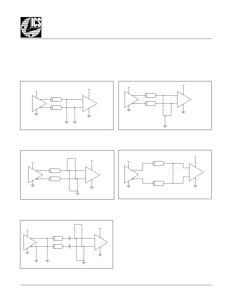
The CLK /nCLK accepts LVDS, LVPECL, LVHSTL, SSTL, HCSL
and other differential signals. Both V
SWING
and V
OH
must meet the
V
PP
and V
CMR
input requirements. Figures 3A to 3E show inter-
face examples for the HiPerClockS CLK/nCLK input driven by
the most common driver types. The input interfaces suggested
F
IGURE
3A. H
I
P
ER
C
LOCK
S CLK/
N
CLK I
NPUT
D
RIVEN
BY
ICS H
I
P
ER
C
LOCK
S LVHSTL D
RIVER
here are examples only. Please consult with the vendor of the
driver component to confirm the driver termination requirements.
For example in
Figure 3A,
the input termination applies for ICS
HiPerClockS LVHSTL drivers. If you are using an LVHSTL driver
from another vendor, use their termination recommendation.
1.8V
R2
50
Input
LVHSTL Driver
ICS
HiPerClockS
R1
50
LVHSTL
3.3V
Zo = 50 Ohm
Zo = 50 Ohm
HiPerClockS
CLK
nCLK
F
IGURE
3E. H
I
P
ER
C
LOCK
S CLK/
N
CLK I
NPUT
D
RIVEN
BY
3.3V LVPECL D
RIVER
WITH
AC C
OUPLE
Zo = 50 Ohm
R3
125
HiPerClockS
CLK
nCLK
3.3V
R5
100 - 200
3.3V
R2
84
3.3V
R6
100 - 200
Input
R5,R6 locate near the driver pin.
Zo = 50 Ohm
R1
84
R4
125
C2
LVPECL
C1
Zo = 50 Ohm
R1
100
3.3V
LVDS_Driv er
Zo = 50 Ohm
Receiv er
CLK
nCLK
3.3V

85314BGI-01
www.icst.com/products/hiperclocks.html
REV. E SEPTEMBER 23, 2005
11
Integrated
Circuit
Systems, Inc.
ICS85314I-01
L
OW
S
KEW
, 1-
TO
-5
D
IFFERENTIAL
-
TO
-2.5V/3.3V LVPECL F
ANOUT
B
UFFER
The clock layout topology shown below is a typical termina-
tion for LVPECL outputs. The two different layouts mentioned
are recommended only as guidelines.
FOUT and nFOUT are low impedance follower outputs that gen-
erate ECL/LVPECL compatible outputs. Therefore, terminating
resistors (DC current path to ground) or current sources must
be used for functionality. These outputs are designed to drive
V
CC
- 2V
50
50
RTT
Z
o
= 50
Z
o
= 50
FOUT
FIN
RTT =
Z
o
1
((V
OH
+ V
OL
) / (V
CC
� 2)) � 2
3.3V
125
125
84
84
Z
o
= 50
Z
o
= 50
FOUT
FIN
50
transmission lines. Matched impedance techniques should
be used to maximize operating frequency and minimize signal
distortion.
Figures 4A and 4B
show two different layouts which
are recommended only as guidelines. Other suitable clock lay-
outs may exist and it would be recommended that the board
designers simulate to guarantee compatibility across all printed
circuit and clock component process variations.
F
IGURE
4B. LVPECL O
UTPUT
T
ERMINATION
F
IGURE
4A. LVPECL O
UTPUT
T
ERMINATION
T
ERMINATION
FOR
3.3V LVPECL O
UTPUTS

85314BGI-01
www.icst.com/products/hiperclocks.html
REV. E SEPTEMBER 23, 2005
12
Integrated
Circuit
Systems, Inc.
ICS85314I-01
L
OW
S
KEW
, 1-
TO
-5
D
IFFERENTIAL
-
TO
-2.5V/3.3V LVPECL F
ANOUT
B
UFFER
T
ERMINATION
FOR
2.5V LVPECL O
UTPUT
Figure 5A
and
Figure 5B
show examples of termination for
2.5V LVPECL driver. These terminations are equivalent to ter-
minating 50
to V
CC
- 2V. For V
CC
= 2.5V, the V
CC
- 2V is very
close to ground level. The R3 in Figure 5B can be eliminated
and the termination is shown in
Figure 5C.
F
IGURE
5C. 2.5V LVPECL T
ERMINATION
E
XAMPLE
F
IGURE
5B. 2.5V LVPECL D
RIVER
T
ERMINATION
E
XAMPLE
F
IGURE
5A. 2.5V LVPECL D
RIVER
T
ERMINATION
E
XAMPLE
R2
62.5
Zo = 50 Ohm
R1
250
+
-
2.5V
2,5V LVPECL
Driv er
R4
62.5
R3
250
Zo = 50 Ohm
2.5V
VCC=2.5V
R1
50
R3
18
Zo = 50 Ohm
Zo = 50 Ohm
+
-
2,5V LVPECL
Driv er
VCC=2.5V
2.5V
R2
50
2,5V LVPECL
Driv er
VCC=2.5V
R1
50
R2
50
2.5V
Zo = 50 Ohm
Zo = 50 Ohm
+
-

85314BGI-01
www.icst.com/products/hiperclocks.html
REV. E SEPTEMBER 23, 2005
13
Integrated
Circuit
Systems, Inc.
ICS85314I-01
L
OW
S
KEW
, 1-
TO
-5
D
IFFERENTIAL
-
TO
-2.5V/3.3V LVPECL F
ANOUT
B
UFFER
P
OWER
C
ONSIDERATIONS
This section provides information on power dissipation and junction temperature for the ICS85314I-01.
Equations and example calculations are also provided.
1. Power Dissipation.
The total power dissipation for the ICS85314I-01 is the sum of the core power plus the power dissipated in the load(s).
The following is the power dissipation for V
CC
= 3.8V, which gives worst case results.
NOTE: Please refer to Section 3 for details on calculating power dissipated in the load.
�
Power (core)
MAX
= V
CC_MAX
* I
EE_MAX
= 3.8V * 80mA = 304mW
�
Power (outputs)
MAX
= 30.2mW/Loaded Output pair
If all outputs are loaded, the total power is 5 * 30.2mW = 151mW
Total Power
_MAX
(3.465V, with all outputs switching) = 304mW + 151mW = 455mW
2. Junction Temperature.
Junction temperature, Tj, is the temperature at the junction of the bond wire and bond pad and directly affects the reliability of the
device. The maximum recommended junction temperature for HiPerClockS
TM
devices is 125�C.
The equation for Tj is as follows: Tj =
JA
* Pd_total + T
A
Tj = Junction Temperature
JA
= Junction-to-Ambient Thermal Resistance
Pd_total = Total Device Power Dissipation (example calculation is in section 1 above)
T
A
= Ambient Temperature
In order to calculate junction temperature, the appropriate junction-to-ambient thermal resistance
JA
must be used. Assuming a
moderate air flow of 200 linear feet per minute and a multi-layer board, the appropriate value is 66.6�C/W per Table 6A below.
Therefore, Tj for an ambient temperature of 85�C with all outputs switching is:
85�C + 0.455W * 66.6�C/W = 115�C. This is well below the limit of 125�C.
This calculation is only an example. Tj will obviously vary depending on the number of loaded outputs, supply voltage, air flow,
and the type of board (single layer or multi-layer).
JA
by Velocity (Linear Feet per Minute)
0
200
500
Single-Layer PCB, JEDEC Standard Test Boards
114.5�C/W
98.0�C/W
88.0�C/W
Multi-Layer PCB, JEDEC Standard Test Boards
73.2�C/W
66.6�C/W
63.5�C/W
NOTE: Most modern PCB designs use multi-layered boards. The data in the second row pertains to most designs.
T
ABLE
6A. T
HERMAL
R
ESISTANCE
JA
FOR
20-
PIN
TSSOP, F
ORCED
C
ONVECTION
JA
by Velocity (Linear Feet per Minute)
0
200
500
Single-Layer PCB, JEDEC Standard Test Boards
83.2�C/W
65.7�C/W
57.5�C/W
Multi-Layer PCB, JEDEC Standard Test Boards
46.2�C/W
39.7�C/W
36.8�C/W
NOTE: Most modern PCB designs use multi-layered boards. The data in the second row pertains to most designs.
T
ABLE
6B. T
HERMAL
R
ESISTANCE
JA
FOR
20-
PIN
SOIC, F
ORCED
C
ONVECTION
85314BGI-01
www.icst.com/products/hiperclocks.html
REV. E SEPTEMBER 23, 2005
14
Integrated
Circuit
Systems, Inc.
ICS85314I-01
L
OW
S
KEW
, 1-
TO
-5
D
IFFERENTIAL
-
TO
-2.5V/3.3V LVPECL F
ANOUT
B
UFFER
3. Calculations and Equations.
LVPECL output driver circuit and termination are shown in
Figure 6.
T
o calculate worst case power dissipation into the load, use the following equations which assume a 50
load, and a termination
voltage of V
CC
- 2V.
�
For logic high, V
OUT
= V
OH_MAX
= V
CC_MAX
� 1.0V
(V
CC_MAX
- V
OH_MAX
) = 1.0V
�
For logic low, V
OUT
= V
OL_MAX
= V
CC_MAX
� 1.7V
(V
CC_MAX
- V
OL_MAX
) = 1.7V
Pd_H is power dissipation when the output drives high.
Pd_L is the power dissipation when the output drives low.
Pd_H = [(V
OH_MAX
� (V
CC_MAX
- 2V))/R
L
] * (V
CC_MAX
- V
OH_MAX
) = [(2V - (V
CC_MAX
- V
OH_MAX
))/R
L
] * (V
CC_MAX
- V
OH_MAX
) =
[(2V - 1V)/50
] * 1V = 20.0mW
Pd_L = [(V
OL_MAX
� (V
CC_MAX
- 2V))/R
L
] * (V
CC_MAX
- V
OL_MAX
) = [(2V - (V
CC_MAX
- V
OL_MAX
))/R
L
] * (V
CC_MAX
- V
OL_MAX
) =
[(2V - 1.7V)/50
] * 1.7V = 10.2mW
Total Power Dissipation per output pair = Pd_H + Pd_L = 30.2mW
F
IGURE
6. LVPECL D
RIVER
C
IRCUIT
AND
T
ERMINATION
Q1
V
OUT
V
CC
RL
50
V
CC
- 2V

85314BGI-01
www.icst.com/products/hiperclocks.html
REV. E SEPTEMBER 23, 2005
15
Integrated
Circuit
Systems, Inc.
ICS85314I-01
L
OW
S
KEW
, 1-
TO
-5
D
IFFERENTIAL
-
TO
-2.5V/3.3V LVPECL F
ANOUT
B
UFFER
R
ELIABILITY
I
NFORMATION
T
RANSISTOR
C
OUNT
The transistor count for ICS85314I-01 is: 674
Compatible to part number MC100LVEL14
T
ABLE
7A.
JA
VS
. A
IR
F
LOW
T
ABLE
FOR
20 L
EAD
TSSOP
JA
by Velocity (Linear Feet per Minute)
0
200
500
Single-Layer PCB, JEDEC Standard Test Boards
114.5�C/W
98.0�C/W
88.0�C/W
Multi-Layer PCB, JEDEC Standard Test Boards
73.2�C/W
66.6�C/W
63.5�C/W
NOTE: Most modern PCB designs use multi-layered boards. The data in the second row pertains to most designs.
0
200
500
Single-Layer PCB, JEDEC Standard Test Boards
83.2�C/W
65.7�C/W
57.5�C/W
Multi-Layer PCB, JEDEC Standard Test Boards
46.2�C/W
39.7�C/W
36.8�C/W
NOTE: Most modern PCB designs use multi-layered boards. The data in the second row pertains to most designs.
T
ABLE
7B.
JA
VS
. A
IR
F
LOW
T
ABLE
FOR
20 L
EAD
SOIC
JA
by Velocity (Linear Feet per Minute)
85314BGI-01
www.icst.com/products/hiperclocks.html
REV. E SEPTEMBER 23, 2005
16
Integrated
Circuit
Systems, Inc.
ICS85314I-01
L
OW
S
KEW
, 1-
TO
-5
D
IFFERENTIAL
-
TO
-2.5V/3.3V LVPECL F
ANOUT
B
UFFER
P
ACKAGE
O
UTLINE
- G S
UFFIX
FOR
20 L
EAD
TSSOP
T
ABLE
8A. P
ACKAGE
D
IMENSIONS
Reference Document: JEDEC Publication 95, MO-153
L
O
B
M
Y
S
s
r
e
t
e
m
i
l
l
i
M
m
u
m
i
n
i
M
m
u
m
i
x
a
M
N
0
2
A
-
-
0
2
.
1
1
A
5
0
.
0
5
1
.
0
2
A
0
8
.
0
5
0
.
1
b
9
1
.
0
0
3
.
0
c
9
0
.
0
0
2
.
0
D
0
4
.
6
0
6
.
6
E
C
I
S
A
B
0
4
.
6
1
E
0
3
.
4
0
5
.
4
e
C
I
S
A
B
5
6
.
0
L
5
4
.
0
5
7
.
0
�
0
�
8
a
a
a
-
-
0
1
.
0
85314BGI-01
www.icst.com/products/hiperclocks.html
REV. E SEPTEMBER 23, 2005
17
Integrated
Circuit
Systems, Inc.
ICS85314I-01
L
OW
S
KEW
, 1-
TO
-5
D
IFFERENTIAL
-
TO
-2.5V/3.3V LVPECL F
ANOUT
B
UFFER
P
ACKAGE
O
UTLINE
- M S
UFFIX
FOR
20 L
EAD
SOIC
T
ABLE
8B. P
ACKAGE
D
IMENSIONS
Reference Document: JEDEC Publication 95, MS-013, MO-119
L
O
B
M
Y
S
s
r
e
t
e
m
i
l
l
i
M
m
u
m
i
n
i
M
m
u
m
i
x
a
M
N
0
2
A
-
-
5
6
.
2
1
A
0
1
.
0
-
-
2
A
5
0
.
2
5
5
.
2
B
3
3
.
0
1
5
.
0
C
8
1
.
0
2
3
.
0
D
0
6
.
2
1
0
0
.
3
1
E
0
4
.
7
0
6
.
7
e
C
I
S
A
B
7
2
.
1
H
0
0
.
0
1
5
6
.
0
1
h
5
2
.
0
5
7
.
0
L
0
4
.
0
7
2
.
1
�
0
�
8

85314BGI-01
www.icst.com/products/hiperclocks.html
REV. E SEPTEMBER 23, 2005
18
Integrated
Circuit
Systems, Inc.
ICS85314I-01
L
OW
S
KEW
, 1-
TO
-5
D
IFFERENTIAL
-
TO
-2.5V/3.3V LVPECL F
ANOUT
B
UFFER
T
ABLE
9. O
RDERING
I
NFORMATION
While the information presented herein has been checked for both accuracy and reliability, Integrated Circuit Systems, Incorporated (ICS) assumes no responsibility for either its use
or for infringement of any patents or other rights of third parties, which would result from its use. No other circuits, patents, or licenses are implied. This product is intended for use
in normal commercial and industrial applications. Any other applications such as those requiring high reliability, or other extraordinary environmental requirements are not
recommended without additional processing by ICS. ICS reserves the right to change any circuitry or specifications without notice. ICS does not authorize or warrant any ICS product
for use in life support devices or critical medical instruments.
The aforementioned trademark, HiPerClockS is a trademark of Integrated Circuit Systems, Inc. or its subsidiaries in the United States and/or other countries.
NOTE: Parts that are ordered with an "LF" suffix to the part number are the Pb-Free configuration and are RoHS compliant.
r
e
b
m
u
N
r
e
d
r
O
/
t
r
a
P
g
n
i
k
r
a
M
e
g
a
k
c
a
P
g
n
i
g
a
k
c
a
P
g
n
i
p
p
i
h
S
e
r
u
t
a
r
e
p
m
e
T
1
0
-
I
G
B
4
1
3
5
8
S
C
I
1
0
I
B
4
1
3
5
8
S
C
I
P
O
S
S
T
d
a
e
l
0
2
e
b
u
t
C
�
5
8
o
t
C
�
0
4
-
T
1
0
-
I
G
B
4
1
3
5
8
S
C
I
1
0
I
B
4
1
3
5
8
S
C
I
P
O
S
S
T
d
a
e
l
0
2
l
e
e
r
&
e
p
a
t
0
0
5
2
C
�
5
8
o
t
C
�
0
4
-
F
L
1
0
-
I
G
B
4
1
3
5
8
S
C
I
L
1
0
I
B
4
1
3
5
S
C
I
P
O
S
S
T
"
e
e
r
F
-
d
a
e
L
"
d
a
e
l
0
2
e
b
u
t
C
�
5
8
o
t
C
�
0
4
-
T
F
L
1
0
-
I
G
B
4
1
3
5
8
S
C
I
L
1
0
I
B
4
1
3
5
S
C
I
P
O
S
S
T
"
e
e
r
F
-
d
a
e
L
"
d
a
e
l
0
2
l
e
e
r
&
e
p
a
t
0
0
5
2
C
�
5
8
o
t
C
�
0
4
-
1
0
-
I
M
B
4
1
3
5
8
S
C
I
1
0
-
I
B
4
1
3
5
8
S
C
I
C
I
O
S
d
a
e
l
0
2
e
b
u
t
C
�
5
8
o
t
C
�
0
4
-
T
1
0
-
I
M
B
4
1
3
5
8
S
C
I
1
0
-
I
B
4
1
3
5
8
S
C
I
C
I
O
S
d
a
e
l
0
2
l
e
e
r
&
e
p
a
t
0
0
0
1
C
�
5
8
o
t
C
�
0
4
-
F
L
1
0
-
I
M
B
4
1
3
5
8
S
C
I
D
B
T
C
I
O
S
"
e
e
r
F
-
d
a
e
L
"
d
a
e
l
0
2
e
b
u
t
C
�
5
8
o
t
C
�
0
4
-
T
F
L
1
0
-
I
M
B
4
1
3
5
8
S
C
I
D
B
T
C
I
O
S
"
e
e
r
F
-
d
a
e
L
"
d
a
e
l
0
2
l
e
e
r
&
e
p
a
t
0
0
0
1
C
�
5
8
o
t
C
�
0
4
-
85314BGI-01
www.icst.com/products/hiperclocks.html
REV. E SEPTEMBER 23, 2005
19
Integrated
Circuit
Systems, Inc.
ICS85314I-01
L
OW
S
KEW
, 1-
TO
-5
D
IFFERENTIAL
-
TO
-2.5V/3.3V LVPECL F
ANOUT
B
UFFER
T
E
E
H
S
Y
R
O
T
S
I
H
N
O
I
S
I
V
E
R
v
e
R
e
l
b
a
T
e
g
a
P
e
g
n
a
h
C
f
o
n
o
i
t
p
i
r
c
s
e
D
e
t
a
D
A
7
8
9
5
1
.
m
a
r
g
a
i
D
l
a
n
g
i
S
d
e
d
n
E
e
l
g
n
i
S
,
2
e
r
u
g
i
F
d
e
t
a
d
p
U
.
n
o
i
t
c
e
s
"
s
t
u
p
t
u
O
L
C
E
P
V
L
V
5
.
2
r
o
f
n
o
i
t
a
n
i
m
r
e
T
"
d
e
d
d
A
.
n
o
i
t
c
e
s
"
e
c
a
f
r
e
t
n
I
t
u
p
n
I
l
a
i
t
n
e
r
e
f
f
i
D
"
d
e
d
d
A
.
B
.
v
e
R
o
t
A
.
v
e
R
m
o
r
f
g
n
i
k
r
a
M
d
n
a
r
e
b
m
u
N
r
e
d
r
O
d
e
t
c
e
r
r
o
C
3
0
/
1
3
/
3
B
2
T
5
T
1
2
5
6
8
9
.
n
o
i
t
c
e
s
s
e
r
u
t
a
e
F
o
t
t
e
ll
u
B
e
s
i
o
N
e
s
a
h
P
d
e
d
d
A
C
d
e
g
n
a
h
C
N
I
.
l
a
c
i
p
y
t
F
p
4
o
t
.
x
a
m
F
p
4
m
o
r
f
.
r
e
t
t
i
J
e
s
a
h
P
S
M
R
d
e
d
d
a
-
e
l
b
a
T
s
c
i
t
s
i
r
e
t
c
a
r
a
h
C
C
A
.
t
o
l
P
r
e
t
t
i
J
e
s
a
h
P
d
e
d
d
A
.
s
m
a
r
g
a
i
d
t
u
p
t
u
O
L
C
E
P
V
L
V
3
.
3
r
o
f
n
o
i
t
a
n
i
m
r
e
T
d
e
t
a
d
p
U
.
n
o
i
t
c
e
s
t
u
p
t
u
O
L
C
E
P
V
L
V
5
.
2
r
o
f
n
o
i
t
a
n
i
m
r
e
T
d
e
t
a
d
p
U
4
0
/
1
1
/
8
C
5
T
1
4
5
7
.
w
e
k
s
t
u
p
t
u
o
e
g
a
k
c
a
p
C
I
O
S
d
e
d
d
a
-
n
o
i
t
c
e
s
s
e
r
u
t
a
e
F
.
e
c
n
a
d
e
p
m
I
l
a
m
r
e
h
T
e
g
a
k
c
a
P
C
I
O
S
d
e
d
d
a
-
s
g
n
i
t
a
R
m
u
m
i
x
a
M
e
t
u
l
o
s
b
A
.
w
e
k
S
t
u
p
t
u
O
r
o
f
e
g
a
k
c
a
p
C
I
O
S
d
e
d
d
a
-
e
l
b
a
t
s
c
i
t
s
i
r
e
t
c
a
r
a
h
C
C
A
S
M
R
d
n
a
w
e
k
S
t
r
a
P
-
o
t
-
t
r
a
P
d
e
d
d
a
-
n
o
i
t
a
m
r
o
f
n
I
t
n
e
m
e
r
u
s
a
e
M
r
e
t
e
m
a
r
a
P
.
s
m
a
r
g
a
i
D
r
e
t
t
i
J
e
s
a
h
P
5
0
/
2
2
/
3
D
5
T
1
5
.
x
a
m
s
p
0
5
3
o
t
.
x
a
m
s
p
0
5
2
m
o
r
f
w
e
k
S
t
r
a
P
-
o
t
-
t
r
a
P
d
e
g
n
a
h
c
-
n
o
i
t
c
e
s
s
e
r
u
t
a
e
F
o
t
.
x
a
m
s
p
0
5
2
m
o
r
f
w
e
k
S
t
r
a
P
-
o
t
-
t
r
a
P
d
e
g
n
a
h
c
-
e
l
b
a
t
s
c
i
t
s
i
r
e
t
c
a
r
a
h
C
C
A
.
x
a
m
s
p
0
5
3
5
0
/
4
2
/
5
E
D
4
T
9
T
5
9
8
1
V
d
e
g
n
a
h
c
-
e
l
b
a
T
s
c
i
t
s
i
r
e
t
c
a
r
a
h
C
C
D
L
C
E
P
V
L
H
O
V
m
o
r
f
x
a
m
C
C
o
t
V
0
.
1
-
V
C
C
.
V
9
.
0
-
d
e
d
d
a
-
n
o
i
t
c
e
S
n
o
i
t
a
m
r
o
f
n
I
n
o
i
t
a
c
il
p
p
A
t
u
p
n
I
d
e
s
u
n
U
r
o
f
s
n
o
i
t
a
d
n
e
m
m
o
c
e
R
.
s
n
i
P
t
u
p
t
u
O
d
n
a
.
r
e
b
m
u
n
t
r
a
p
e
e
r
F
-
d
a
e
L
P
O
S
S
T
d
e
d
d
A
5
0
/
3
2
/
9