Document Outline
- General Description
- Features
- Block Diagram
- Pin Assignment
- Pin Descriptions
- Pin Characteristics
- Absolute Maximum Ratings
- Power Supply 3.3V DC Characteristics
- LVCMOS 3.3V DC Characteristics
- LVPECL 3.3V DC Characteristics
- 3.3V AC Characteristics
- Power Supply 2.5V DC Characteristics
- LVCMOS 2.5V DC Characteristics
- LVPECL 2.5V DC Characteristics
- 2.5V AC Characteristics
- Parameter Measurement Information
- 3.3V Output Load AC Test Circuit Diagram
- 2.5V Output Load AC Test Circuit Diagram
- Part-to-Part Skew Diagram
- Propagation Delay Diagram
- Output Rise/Fall Time Diagram
- Output Duty Cyle/Pulse Width/Period Diagram
- Application Information
- Termination for 3.3V LVPECL Outputs
- Termination for 2.5V LVPECL Outputs
- Power Consideraitons
- Power Dissipation
- Junction Temperature
- Thermal Resistance
- Calculations & Equations
- LVPECL Driver Circuit & Termination Diagram
- Reliability Information
- Transistor Count
- Package Outline
- Package Dimensions
- Ordering Information
- Revision History Sheet
85322AMI
www.icst.com/products/hiperclocks.html
REV. B OCTOBER 7, 2003
1
Integrated
Circuit
Systems, Inc.
ICS85322I
D
UAL
LVCMOS / LVTTL-
TO
-D
IFFERENTIAL
2.5V / 3.3V LVPECL T
RANSLATOR
G
ENERAL
D
ESCRIPTION
The ICS85322I is a Dual LVCMOS / LVTTL-to-
Differential 2.5V / 3.3V LVPECL translator and a
member of the HiPerClocksTM family of High Per-
for mance Clocks Solutions from ICS. The
ICS85322I has selectable single ended clock in-
puts. The single ended clock input accepts LVCMOS or LVTTL
input levels and translate them to 2.5V / 3.3V LVPECL levels.
The small outline 8-pin SOIC package makes this device ideal
for applications where space, high performance and low power
are important.
F
EATURES
� 2 differential 2.5V/3.3V LVPECL outputs
� Selectable CLK0, CLK1 LVCMOS/LVTTL clock inputs
� CLK0 and CLK1 can accepts the following input levels:
LVCMOS or LVTTL
� Maximum output frequency: 267MHz
� Part-to-part skew: 250ps (maximum)
� 3.3V operating supply voltage
(operating range 3.135V to 3.465V)
� 2.5V operating supply voltage
(operating range 2.375V to 2.625V)
� -40�C to 85�C ambient operating temperature
B
LOCK
D
IAGRAM
P
IN
A
SSIGNMENT
ICS85322I
8-Lead SOIC
3.90mm x 4.92mm x 1.37mm body package
M Package
Top View
Q0
nQ0
Q1
nQ1
1
2
3
4
Q0
nQ0
Q1
nQ1
CLK0
CLK1
HiPerClockSTM
ICS
V
CC
CLK0
CLK1
V
EE
8
7
6
5
85322AMI
www.icst.com/products/hiperclocks.html
REV. B OCTOBER 7, 2003
2
Integrated
Circuit
Systems, Inc.
ICS85322I
D
UAL
LVCMOS / LVTTL-
TO
-D
IFFERENTIAL
2.5V / 3.3V LVPECL T
RANSLATOR
T
ABLE
1. P
IN
D
ESCRIPTIONS
T
ABLE
2. P
IN
C
HARACTERISTICS
r
e
b
m
u
N
e
m
a
N
e
p
y
T
n
o
i
t
p
i
r
c
s
e
D
2
,
1
0
Q
n
,
0
Q
t
u
p
t
u
O
.
s
l
e
v
e
l
e
c
a
f
r
e
t
n
i
L
C
E
P
V
L
.
r
i
a
p
t
u
p
t
u
o
l
a
i
t
n
e
r
e
f
f
i
D
4
,
3
1
Q
n
,
1
Q
t
u
p
t
u
O
.
s
l
e
v
e
l
e
c
a
f
r
e
t
n
i
L
C
E
P
V
L
.
r
i
a
p
t
u
p
t
u
o
l
a
i
t
n
e
r
e
f
f
i
D
5
V
E
E
r
e
w
o
P
.
n
i
p
y
l
p
p
u
s
e
v
i
t
a
g
e
N
6
1
K
L
C
t
u
p
n
I
p
u
ll
u
P
.
t
u
p
n
i
k
c
o
l
c
L
T
T
V
L
/
S
O
M
C
V
L
7
0
K
L
C
t
u
p
n
I
p
u
ll
u
P
.
t
u
p
n
i
k
c
o
l
c
L
T
T
V
L
/
S
O
M
C
V
L
8
V
C
C
r
e
w
o
P
.
n
i
p
y
l
p
p
u
s
e
v
i
t
i
s
o
P
:
E
T
O
N
p
u
ll
u
P
.
s
e
u
l
a
v
l
a
c
i
p
y
t
r
o
f
,
s
c
i
t
s
i
r
e
t
c
a
r
a
h
C
n
i
P
,
2
e
l
b
a
T
e
e
S
.
s
r
o
t
s
i
s
e
r
t
u
p
n
i
l
a
n
r
e
t
n
i
o
t
s
r
e
f
e
r
l
o
b
m
y
S
r
e
t
e
m
a
r
a
P
s
n
o
i
t
i
d
n
o
C
t
s
e
T
m
u
m
i
n
i
M
l
a
c
i
p
y
T
m
u
m
i
x
a
M
s
t
i
n
U
C
N
I
e
c
n
a
t
i
c
a
p
a
C
t
u
p
n
I
4
F
p
R
P
U
L
L
U
P
r
o
t
s
i
s
e
R
p
u
ll
u
P
t
u
p
n
I
1
5
K
R
N
W
O
D
L
L
U
P
r
o
t
s
i
s
e
R
n
w
o
d
ll
u
P
t
u
p
n
I
1
5
K

85322AMI
www.icst.com/products/hiperclocks.html
REV. B OCTOBER 7, 2003
3
Integrated
Circuit
Systems, Inc.
ICS85322I
D
UAL
LVCMOS / LVTTL-
TO
-D
IFFERENTIAL
2.5V / 3.3V LVPECL T
RANSLATOR
T
ABLE
3A. P
OWER
S
UPPLY
DC C
HARACTERISTICS
,
V
CC
= 3.3V�5%, T
A
= -40�C
TO
85�C
T
ABLE
3B. LVCMOS / LVTTL DC C
HARACTERISTICS
,
V
CC
= 3.3V�5%, T
A
= -40�C
TO
85�C
l
o
b
m
y
S
r
e
t
e
m
a
r
a
P
s
n
o
i
t
i
d
n
o
C
t
s
e
T
m
u
m
i
n
i
M
l
a
c
i
p
y
T
m
u
m
i
x
a
M
s
t
i
n
U
V
C
C
e
g
a
t
l
o
V
y
l
p
p
u
S
e
v
i
t
i
s
o
P
5
3
1
.
3
3
.
3
5
6
4
.
3
V
I
E
E
t
n
e
r
r
u
C
y
l
p
p
u
S
r
e
w
o
P
5
2
A
m
l
o
b
m
y
S
r
e
t
e
m
a
r
a
P
s
n
o
i
t
i
d
n
o
C
t
s
e
T
m
u
m
i
n
i
M
l
a
c
i
p
y
T
m
u
m
i
x
a
M
s
t
i
n
U
V
H
I
e
g
a
t
l
o
V
h
g
i
H
t
u
p
n
I
1
K
L
C
,
0
K
L
C
2
V
C
C
3
.
0
+
V
V
L
I
e
g
a
t
l
o
V
w
o
L
t
u
p
n
I
1
K
L
C
,
0
K
L
C
3
.
0
-
3
.
1
V
I
H
I
t
n
e
r
r
u
C
h
g
i
H
t
u
p
n
I
1
K
L
C
,
0
K
L
C
V
C
C
V
=
N
I
V
5
6
4
.
3
=
5
A
�
I
L
I
t
n
e
r
r
u
C
w
o
L
t
u
p
n
I
1
K
L
C
,
0
K
L
C
V
C
C
V
=
N
I
V
5
6
4
.
3
=
0
5
1
-
A
�
T
ABLE
3C. LVPECL DC C
HARACTERISTICS
,
V
CC
= 3.3V�5%, T
A
= -40�C
TO
85�C
l
o
b
m
y
S
r
e
t
e
m
a
r
a
P
s
n
o
i
t
i
d
n
o
C
t
s
e
T
m
u
m
i
n
i
M
l
a
c
i
p
y
T
m
u
m
i
x
a
M
s
t
i
n
U
V
H
O
1
E
T
O
N
;
e
g
a
t
l
o
V
h
g
i
H
t
u
p
t
u
O
V
C
C
V
=
N
I
V
5
6
4
.
3
=
V
C
C
4
.
1
-
V
C
C
0
.
1
-
V
V
L
O
1
E
T
O
N
;
e
g
a
t
l
o
V
w
o
L
t
u
p
t
u
O
V
C
C
V
=
N
I
V
5
6
4
.
3
=
V
C
C
0
.
2
-
V
C
C
7
.
1
-
V
V
G
N
I
W
S
g
n
i
w
S
e
g
a
t
l
o
V
t
u
p
t
u
O
k
a
e
P
-
o
t
-
k
a
e
P
5
6
.
0
9
.
0
V
0
5
h
t
i
w
d
e
t
a
n
i
m
r
e
t
s
t
u
p
t
u
O
:
1
E
T
O
N
V
o
t
C
C
.
V
2
-
A
BSOLUTE
M
AXIMUM
R
ATINGS
Supply Voltage, V
CC
4.6V
Inputs, V
I
-0.5V to V
CC
+ 0.5 V
Outputs, I
O
Continuous Current
50mA
Surge Current
100mA
Package Thermal Impedance,
JA
112.7�C/W (0 lfpm)
Storage Temperature, T
STG
-65�C to 150�C
NOTE: Stresses beyond those listed under Absolute
Maximum Ratings may cause permanent damage to the
device. These ratings are stress specifications only. Functional
operation of product at these conditions or any conditions be-
yond those listed in the
DC Characteristics or AC Character-
istics is not implied. Exposure to absolute maximum rating
conditions for extended periods may affect product reliability.
T
ABLE
4A. AC C
HARACTERISTICS
,
V
CC
= 3.3V�5%, T
A
= -40�C
TO
85�C
l
o
b
m
y
S
r
e
t
e
m
a
r
a
P
s
n
o
i
t
i
d
n
o
C
t
s
e
T
m
u
m
i
n
i
M
l
a
c
i
p
y
T
m
u
m
i
x
a
M
s
t
i
n
U
f
X
A
M
y
c
n
e
u
q
e
r
F
t
u
p
t
u
O
7
6
2
z
H
M
t
D
P
1
E
T
O
N
;
y
a
l
e
D
n
o
i
t
a
g
a
p
o
r
P
z
H
M
7
6
2
5
.
0
9
.
1
s
n
t
)
p
p
(
k
s
3
,
2
E
T
O
N
;
w
e
k
S
t
r
a
P
-
o
t
-
t
r
a
P
0
5
2
s
p
t
R
t
/
F
e
m
i
T
ll
a
F
/
e
s
i
R
t
u
p
t
u
O
z
H
M
0
5
@
%
0
8
o
t
%
0
2
0
0
3
0
0
7
s
p
c
d
o
e
l
c
y
C
y
t
u
D
t
u
p
t
u
O
0
4
0
6
%
.
e
s
i
w
r
e
h
t
o
d
e
t
o
n
s
s
e
l
n
u
z
H
M
3
3
1
t
a
d
e
r
u
s
a
e
m
s
r
e
t
e
m
a
r
a
p
ll
A
V
m
o
r
f
d
e
r
u
s
a
e
M
:
1
E
T
O
N
C
C
.
t
n
i
o
p
g
n
i
s
s
o
r
c
t
u
p
t
u
o
l
a
i
t
n
e
r
e
f
f
i
d
e
h
t
o
t
t
u
p
n
i
e
h
t
f
o
t
n
i
o
p
2
/
d
a
o
l
l
a
u
q
e
h
t
i
w
d
n
a
s
e
g
a
t
l
o
v
y
l
p
p
u
s
e
m
a
s
e
h
t
t
a
g
n
i
t
a
r
e
p
o
s
e
c
i
v
e
d
t
n
e
r
e
f
f
i
d
n
o
s
t
u
p
t
u
o
n
e
e
w
t
e
b
w
e
k
s
s
a
d
e
n
i
f
e
D
:
2
E
T
O
N
.
s
t
n
i
o
p
s
s
o
r
c
l
a
i
t
n
e
r
e
f
f
i
d
e
h
t
t
a
d
e
r
u
s
a
e
m
e
r
a
s
t
u
p
t
u
o
e
h
t
,
e
c
i
v
e
d
h
c
a
e
n
o
s
t
u
p
n
i
f
o
e
p
y
t
e
m
a
s
e
h
t
g
n
i
s
U
.
s
n
o
i
t
i
d
n
o
c
.
5
6
d
r
a
d
n
a
t
S
C
E
D
E
J
h
t
i
w
e
c
n
a
d
r
o
c
c
a
n
i
d
e
n
i
f
e
d
s
i
r
e
t
e
m
a
r
a
p
s
i
h
T
:
3
E
T
O
N
85322AMI
www.icst.com/products/hiperclocks.html
REV. B OCTOBER 7, 2003
4
Integrated
Circuit
Systems, Inc.
ICS85322I
D
UAL
LVCMOS / LVTTL-
TO
-D
IFFERENTIAL
2.5V / 3.3V LVPECL T
RANSLATOR
T
ABLE
3D. P
OWER
S
UPPLY
DC C
HARACTERISTICS
,
V
CC
= 2.5V�5%, T
A
= -40�C
TO
85�C
T
ABLE
3E. LVCMOS / LVTTL DC C
HARACTERISTICS
,
V
CC
= 2.5V�5%, T
A
= -40�C
TO
85�C
l
o
b
m
y
S
r
e
t
e
m
a
r
a
P
s
n
o
i
t
i
d
n
o
C
t
s
e
T
m
u
m
i
n
i
M
l
a
c
i
p
y
T
m
u
m
i
x
a
M
s
t
i
n
U
V
C
C
e
g
a
t
l
o
V
y
l
p
p
u
S
e
v
i
t
i
s
o
P
5
7
3
.
2
5
.
2
5
2
6
.
2
V
I
E
E
t
n
e
r
r
u
C
y
l
p
p
u
S
r
e
w
o
P
5
2
A
m
l
o
b
m
y
S
r
e
t
e
m
a
r
a
P
s
n
o
i
t
i
d
n
o
C
t
s
e
T
m
u
m
i
n
i
M
l
a
c
i
p
y
T
m
u
m
i
x
a
M
s
t
i
n
U
V
H
I
e
g
a
t
l
o
V
h
g
i
H
t
u
p
n
I
1
K
L
C
,
0
K
L
C
6
.
1
V
C
C
3
.
0
+
V
V
L
I
e
g
a
t
l
o
V
w
o
L
t
u
p
n
I
1
K
L
C
,
0
K
L
C
3
.
0
-
9
.
0
V
I
H
I
t
n
e
r
r
u
C
h
g
i
H
t
u
p
n
I
1
K
L
C
,
0
K
L
C
V
C
C
V
=
N
I
5
2
6
.
2
=
5
A
�
I
L
I
t
n
e
r
r
u
C
w
o
L
t
u
p
n
I
1
K
L
C
,
0
K
L
C
V
C
C
V
=
N
I
5
2
6
.
2
=
0
5
1
-
A
�
T
ABLE
3F. LVPECL DC C
HARACTERISTICS
,
V
CC
= 2.5V�5%, T
A
= -40�C
TO
85�C
l
o
b
m
y
S
r
e
t
e
m
a
r
a
P
s
n
o
i
t
i
d
n
o
C
t
s
e
T
m
u
m
i
n
i
M
l
a
c
i
p
y
T
m
u
m
i
x
a
M
s
t
i
n
U
V
H
O
1
E
T
O
N
;
e
g
a
t
l
o
V
h
g
i
H
t
u
p
t
u
O
V
C
C
4
.
1
-
V
C
C
0
.
1
-
V
V
L
O
1
E
T
O
N
;
e
g
a
t
l
o
V
w
o
L
t
u
p
t
u
O
V
C
C
0
.
2
-
V
C
C
7
.
1
-
V
V
G
N
I
W
S
g
n
i
w
S
e
g
a
t
l
o
V
t
u
p
t
u
O
k
a
e
P
-
o
t
-
k
a
e
P
5
6
.
0
9
.
0
V
0
5
h
t
i
w
d
e
t
a
n
i
m
r
e
t
s
t
u
p
t
u
O
:
1
E
T
O
N
V
o
t
C
C
.
V
2
-
T
ABLE
4B. AC C
HARACTERISTICS
,
V
CC
= 2.5V�5%, T
A
= -40�C
TO
85�C
l
o
b
m
y
S
r
e
t
e
m
a
r
a
P
s
n
o
i
t
i
d
n
o
C
t
s
e
T
m
u
m
i
n
i
M
l
a
c
i
p
y
T
m
u
m
i
x
a
M
s
t
i
n
U
f
X
A
M
y
c
n
e
u
q
e
r
F
t
u
p
t
u
O
5
1
2
z
H
M
t
D
P
1
E
T
O
N
;
y
a
l
e
D
n
o
i
t
a
g
a
p
o
r
P
z
H
M
5
1
2
7
.
0
1
.
2
s
n
t
)
p
p
(
k
s
3
,
2
E
T
O
N
;
w
e
k
S
t
r
a
P
-
o
t
-
t
r
a
P
0
5
2
s
p
t
R
t
/
F
e
m
i
T
ll
a
F
/
e
s
i
R
t
u
p
t
u
O
z
H
M
0
5
@
%
0
8
o
t
%
0
2
0
0
3
0
0
7
s
p
c
d
o
e
l
c
y
C
y
t
u
D
t
u
p
t
u
O
0
4
0
6
%
.
e
s
i
w
r
e
h
t
o
d
e
t
o
n
s
s
e
l
n
u
z
H
M
3
3
1
t
a
d
e
r
u
s
a
e
m
s
r
e
t
e
m
a
r
a
p
ll
A
V
m
o
r
f
d
e
r
u
s
a
e
M
:
1
E
T
O
N
C
C
.
t
n
i
o
p
g
n
i
s
s
o
r
c
t
u
p
t
u
o
l
a
i
t
n
e
r
e
f
f
i
d
e
h
t
o
t
t
u
p
n
i
e
h
t
f
o
t
n
i
o
p
2
/
d
a
o
l
l
a
u
q
e
h
t
i
w
d
n
a
s
e
g
a
t
l
o
v
y
l
p
p
u
s
e
m
a
s
e
h
t
t
a
g
n
i
t
a
r
e
p
o
s
e
c
i
v
e
d
t
n
e
r
e
f
f
i
d
n
o
s
t
u
p
t
u
o
n
e
e
w
t
e
b
w
e
k
s
s
a
d
e
n
i
f
e
D
:
2
E
T
O
N
.
s
t
n
i
o
p
s
s
o
r
c
l
a
i
t
n
e
r
e
f
f
i
d
e
h
t
t
a
d
e
r
u
s
a
e
m
e
r
a
s
t
u
p
t
u
o
e
h
t
,
e
c
i
v
e
d
h
c
a
e
n
o
s
t
u
p
n
i
f
o
e
p
y
t
e
m
a
s
e
h
t
g
n
i
s
U
.
s
n
o
i
t
i
d
n
o
c
.
.
5
6
d
r
a
d
n
a
t
S
C
E
D
E
J
h
t
i
w
e
c
n
a
d
r
o
c
c
a
n
i
d
e
n
i
f
e
d
s
i
r
e
t
e
m
a
r
a
p
s
i
h
T
:
3
E
T
O
N
85322AMI
www.icst.com/products/hiperclocks.html
REV. B OCTOBER 7, 2003
5
Integrated
Circuit
Systems, Inc.
ICS85322I
D
UAL
LVCMOS / LVTTL-
TO
-D
IFFERENTIAL
2.5V / 3.3V LVPECL T
RANSLATOR
P
ARAMETER
M
EASUREMENT
I
NFORMATION
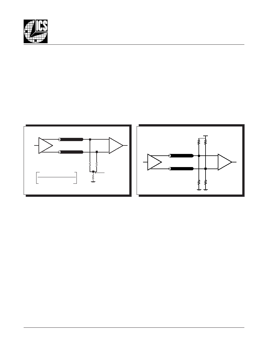
P
ART
-
TO
-P
ART
S
KEW
2.5V O
UTPUT
L
OAD
AC T
EST
C
IRCUIT
3.3V O
UTPUT
L
OAD
AC T
EST
C
IRCUIT
SCOPE
Qx
nQx
LVPECL
2V
t
PD
P
ROPAGATION
D
ELAY
O
UTPUT
R
ISE
/F
ALL
T
IME
O
UTPUT
D
UTY
C
YCLE
/P
ULSE
W
IDTH
/P
ERIOD
-1.3V � 0.165V
t
sk(o)
nQx
Qx
nQy
Qy
Clock
Outputs
20%
80%
80%
20%
t
R
t
F
V
SW I N G
Pulse Width
t
PERIOD
t
PW
t
PERIOD
odc =
Q0, Q1
nQ0, nQ1
CLK0,
CLK1
Q0, Q1
nQ0, nQ1
SCOPE
Qx
nQx
LVPECL
2V
-0.5V � 0.125V
PART 1
PART 2
V
CC
V
EE
V
CC
V
EE
85322AMI
www.icst.com/products/hiperclocks.html
REV. B OCTOBER 7, 2003
6
Integrated
Circuit
Systems, Inc.
ICS85322I
D
UAL
LVCMOS / LVTTL-
TO
-D
IFFERENTIAL
2.5V / 3.3V LVPECL T
RANSLATOR
A
PPLICATION
I
NFORMATION
V
CC
- 2V
50
50
RTT
Z
o
= 50
Z
o
= 50
FOUT
FIN
RTT =
Z
o
1
(V
OH
+ V
OL
/ V
CC
� 2) � 2
3.3V
125
125
84
84
Z
o
= 50
Z
o
= 50
FOUT
FIN
The clock layout topology shown below is a typical termina-
tion for LVPECL outputs. The two different layouts mentioned
are recommended only as guidelines.
FOUT and nFOUT are low impedance follower outputs that gen-
erate ECL/LVPECL compatible outputs. Therefore, terminating
resistors (DC current path to ground) or current sources must
be used for functionality. These outputs are designed to drive
50
transmission lines. Matched impedance techniques should
be used to maximize operating frequency and minimize signal
distortion.
Figures 1A and 1B show two different layouts which
are recommended only as guidelines. Other suitable clock lay-
outs may exist and it would be recommended that the board
designers simulate to guarantee compatibility across all printed
circuit and clock component process variations.
T
ERMINATION
FOR
3.3V LVPECL O
UTPUTS
F
IGURE
1B. LVPECL O
UTPUT
T
ERMINATION
F
IGURE
1A. LVPECL O
UTPUT
T
ERMINATION
85322AMI
www.icst.com/products/hiperclocks.html
REV. B OCTOBER 7, 2003
7
Integrated
Circuit
Systems, Inc.
ICS85322I
D
UAL
LVCMOS / LVTTL-
TO
-D
IFFERENTIAL
2.5V / 3.3V LVPECL T
RANSLATOR
T
ERMINATION
FOR
2.5V LVPECL O
UTPUT
Figure 2A and Figure 2B show examples of termination for 2.5V
LVPECL driver. These terminations are equivalent to terminat-
ing 50
to V
CC
- 2V. For V
CC
= 2.5V, the V
CC
- 2V is very close to
ground level. The R3 in Figure 2B can be eliminated and the
termination is shown in
Figure 2C.
F
IGURE
2C. 2.5V LVPECL T
ERMINATION
E
XAMPLE
R2
50
Zo = 50 Ohm
VCCO=2.5V
R1
50
Zo = 50 Ohm
+
-
2.5V
2,5V LVPECL
Driv er
F
IGURE
2B. 2.5V LVPECL D
RIVER
T
ERMINATION
E
XAMPLE
VCCO=2.5V
R1
50
R2
50
Zo = 50 Ohm
R3
18
2,5V LVPECL
Driv er
Zo = 50 Ohm
+
-
2.5V
F
IGURE
2A. 2.5V LVPECL D
RIVER
T
ERMINATION
E
XAMPLE
R2
62.5
2.5V
2,5V LVPECL
Driv er
R3
250
Zo = 50 Ohm
Zo = 50 Ohm
R4
62.5
2.5V
+
-
R1
250
VCCO=2.5V

85322AMI
www.icst.com/products/hiperclocks.html
REV. B OCTOBER 7, 2003
8
Integrated
Circuit
Systems, Inc.
ICS85322I
D
UAL
LVCMOS / LVTTL-
TO
-D
IFFERENTIAL
2.5V / 3.3V LVPECL T
RANSLATOR
P
OWER
C
ONSIDERATIONS
This section provides information on power dissipation and junction temperature for the ICS85322I.
Equations and example calculations are also provided.
1. Power Dissipation.
The total power dissipation for the ICS85322I is the sum of the core power plus the power dissipated in the load(s).
The following is the power dissipation for V
CC
= 3.3V + 5% = 3.465V, which gives worst case results.
NOTE: Please refer to Section 3 for details on calculating power dissipated in the load.
�
Power (core)
MAX
= V
CC_MAX
* I
EE_MAX
= 3.465V * 25mA = 86.6mW
�
Power (outputs)
MAX
= 30.2mW/Loaded Output pair
If all outputs are loaded, the total power is 2 * 30.2mW = 60.4mW
Total Power
_MAX
(3.465V, with all outputs switching) = 86.6mW + 60.4mW = 147mW
2. Junction Temperature.
Junction temperature, Tj, is the temperature at the junction of the bond wire and bond pad and directly affects the reliability of the
device. The maximum recommended junction temperature for HiPerClockS
TM
devices is 125�C.
The equation for Tj is as follows: Tj =
JA
* Pd_total + T
A
Tj = Junction Temperature
JA
= Junction-to-Ambient Thermal Resistance
Pd_total = Total Device Power Dissipation (example calculation is in section 1 above)
T
A
= Ambient Temperature
In order to calculate junction temperature, the appropriate junction-to-ambient thermal resistance
JA
must be used. Assuming a
moderate air flow of 200 linear feet per minute and a multi-layer board, the appropriate value is 103.3�C/W per Table 5 below.
Therefore, Tj for an ambient temperature of 85�C with all outputs switching is:
85�C + 0.147W * 103.3�C/W = 100.2�C. This is well below the limit of 125�C.
This calculation is only an example. Tj will obviously vary depending on the number of loaded outputs, supply voltage, air flow,
and the type of board (single layer or multi-layer).
JA
by Velocity (Linear Feet per Minute)
0
200
500
Single-Layer PCB, JEDEC Standard Test Boards
153.3�C/W
128.5�C/W
115.5�C/W
Multi-Layer PCB, JEDEC Standard Test Boards
112.7�C/W
103.3�C/W
97.1�C/W
NOTE: Most modern PCB designs use multi-layered boards. The data in the second row pertains to most designs.
T
ABLE
5. T
HERMAL
R
ESISTANCE
JA
FOR
8-
PIN
SOIC, F
ORCED
C
ONVECTION

85322AMI
www.icst.com/products/hiperclocks.html
REV. B OCTOBER 7, 2003
9
Integrated
Circuit
Systems, Inc.
ICS85322I
D
UAL
LVCMOS / LVTTL-
TO
-D
IFFERENTIAL
2.5V / 3.3V LVPECL T
RANSLATOR
3. Calculations and Equations.
The purpose of this section is to derive the power dissipated into the load.
LVPECL output driver circuit and termination are shown in
Figure 3.
T
o calculate worst case power dissipation into the load, use the following equations which assume a 50
load, and a termination
voltage of V
CC
- 2V.
�
For logic high, V
OUT
= V
OH_MAX
= V
CC_MAX
� 1.0V
(V
CC_MAX
- V
OH_MAX
) = 1.0V
�
For logic low, V
OUT
= V
OL_MAX
= V
CC_MAX
� 1.7V
(V
CC_MAX
- V
OL_MAX
) = 1.7V
Pd_H is power dissipation when the output drives high.
Pd_L is the power dissipation when the output drives low.
Pd_H = [(V
OH_MAX
� (V
CC_MAX
- 2V))/R
L
] * (V
CC_MAX
- V
OH_MAX
) = [(2V - (V
CC_MAX
- V
OH_MAX
))/R
L
] * (V
CC_MAX
- V
OH_MAX
) =
[(2V - 1V)/50
] * 1V = 20.0mW
Pd_L = [(V
OL_MAX
� (V
CC_MAX
- 2V))/R
L
] * (V
CC_MAX
- V
OL_MAX
) = [(2V - (V
CC_MAX
- V
OL_MAX
))/R
L
] * (V
CC_MAX
- V
OL_MAX
) =
[(2V - 1.7V)/50
] * 1.7V = 10.2mW
Total Power Dissipation per output pair = Pd_H + Pd_L = 30.2mW
F
IGURE
3. LVPECL D
RIVER
C
IRCUIT
AND
T
ERMINATION
Q1
V
OUT
V
CC
RL
50
V
CC
- 2V

85322AMI
www.icst.com/products/hiperclocks.html
REV. B OCTOBER 7, 2003
10
Integrated
Circuit
Systems, Inc.
ICS85322I
D
UAL
LVCMOS / LVTTL-
TO
-D
IFFERENTIAL
2.5V / 3.3V LVPECL T
RANSLATOR
R
ELIABILITY
I
NFORMATION
T
RANSISTOR
C
OUNT
The transistor count for ICS85322I is: 269
T
ABLE
6.
JA
VS
. A
IR
F
LOW
T
ABLE
FOR
8 L
EAD
SOIC
JA
by Velocity (Linear Feet per Minute)
0
200
500
Single-Layer PCB, JEDEC Standard Test Boards
153.3�C/W
128.5�C/W
115.5�C/W
Multi-Layer PCB, JEDEC Standard Test Boards
112.7�C/W
103.3�C/W
97.1�C/W
NOTE: Most modern PCB designs use multi-layered boards. The data in the second row pertains to most designs.

85322AMI
www.icst.com/products/hiperclocks.html
REV. B OCTOBER 7, 2003
11
Integrated
Circuit
Systems, Inc.
ICS85322I
D
UAL
LVCMOS / LVTTL-
TO
-D
IFFERENTIAL
2.5V / 3.3V LVPECL T
RANSLATOR
P
ACKAGE
O
UTLINE
- M S
UFFIX
FOR
8 L
EAD
SOIC
T
ABLE
7. P
ACKAGE
D
IMENSIONS
Reference Document: JEDEC Publication 95, MS-012
L
O
B
M
Y
S
s
r
e
t
e
m
i
l
l
i
M
N
U
M
I
N
I
M
M
U
M
I
X
A
M
N
8
A
5
3
.
1
5
7
.
1
1
A
0
1
.
0
5
2
.
0
B
3
3
.
0
1
5
.
0
C
9
1
.
0
5
2
.
0
D
0
8
.
4
0
0
.
5
E
0
8
.
3
0
0
.
4
e
C
I
S
A
B
7
2
.
1
H
0
8
.
5
0
2
.
6
h
5
2
.
0
0
5
.
0
L
0
4
.
0
7
2
.
1
�
0
�
8

85322AMI
www.icst.com/products/hiperclocks.html
REV. B OCTOBER 7, 2003
12
Integrated
Circuit
Systems, Inc.
ICS85322I
D
UAL
LVCMOS / LVTTL-
TO
-D
IFFERENTIAL
2.5V / 3.3V LVPECL T
RANSLATOR
T
ABLE
8. O
RDERING
I
NFORMATION
While the information presented herein has been checked for both accuracy and reliability, Integrated Circuit Systems, Incorporated (ICS) assumes no responsibility for either its use
or for infringement of any patents or other rights of third parties, which would result from its use. No other circuits, patents, or licenses are implied. This product is intended for use
in normal commercial and industrial applications. Any other applications such as those requiring high reliability, or other extraordinary environmental requirements are not
recommended without additional processing by ICS. ICS reserves the right to change any circuitry or specifications without notice. ICS does not authorize or warrant any ICS product
for use in life support devices or critical medical instruments.
r
e
b
m
u
N
r
e
d
r
O
/
t
r
a
P
g
n
i
k
r
a
M
e
g
a
k
c
a
P
t
n
u
o
C
e
r
u
t
a
r
e
p
m
e
T
I
M
A
2
2
3
5
8
S
C
I
I
M
A
2
2
3
5
C
I
O
S
d
a
e
l
8
e
b
u
t
r
e
p
6
9
C
�
5
8
o
t
C
�
0
4
-
T
I
M
A
2
2
3
5
8
S
C
I
I
M
A
2
2
3
5
l
e
e
R
d
n
a
e
p
a
T
n
o
C
I
O
S
d
a
e
l
8
0
0
5
2
C
�
5
8
o
t
C
�
0
4
-
85322AMI
www.icst.com/products/hiperclocks.html
REV. B OCTOBER 7, 2003
13
Integrated
Circuit
Systems, Inc.
ICS85322I
D
UAL
LVCMOS / LVTTL-
TO
-D
IFFERENTIAL
2.5V / 3.3V LVPECL T
RANSLATOR
T
E
E
H
S
Y
R
O
T
S
I
H
N
O
I
S
I
V
E
R
v
e
R
e
l
b
a
T
e
g
a
P
e
g
n
a
h
C
f
o
n
o
i
t
p
i
r
c
s
e
D
e
t
a
D
A
8
.
n
o
i
t
c
e
s
s
t
u
p
t
u
O
L
C
E
P
V
L
r
o
f
n
o
i
t
a
n
i
m
r
e
T
d
e
d
d
A
2
0
/
0
3
/
5
A
6
7
V
d
e
t
c
e
r
r
o
c
,
m
a
r
g
a
i
D
t
i
u
c
r
i
C
t
s
e
T
d
a
o
L
t
u
p
t
u
O
V
3
.
3
E
E
V
5
3
1
.
0
�
V
3
.
1
-
=
V
d
a
e
r
o
t
E
E
.
V
5
6
1
.
0
�
V
3
.
1
-
=
.
m
a
r
g
a
i
D
e
m
i
T
ll
a
F
/
e
s
i
R
t
u
p
t
u
O
d
e
t
a
d
p
U
2
0
/
3
2
/
8
B
2
T
2
3
6
7
C
d
e
g
n
a
h
c
-
e
l
b
a
T
s
c
i
t
s
i
r
e
t
c
a
r
a
h
C
n
i
P
N
I
.
l
a
c
i
p
y
t
F
p
4
o
t
.
x
a
m
F
p
4
.
s
g
n
i
t
a
r
s
t
u
p
n
I
d
e
t
a
d
p
u
,
s
g
n
i
t
a
R
m
u
m
i
x
a
M
e
t
u
l
o
s
b
A
.
s
m
a
r
g
a
i
D
n
o
i
t
a
n
i
m
r
e
T
t
u
p
t
u
O
L
C
E
P
V
L
V
3
.
3
d
e
t
a
d
p
U
.
s
t
u
p
t
u
O
L
C
E
P
V
L
V
5
.
2
r
o
f
n
o
i
t
a
n
i
m
r
e
T
d
e
d
d
A
.
t
e
e
h
s
a
t
a
d
t
u
o
h
g
u
o
r
h
t
t
a
m
r
o
f
d
e
t
a
d
p
U
3
0
/
7
/
0
1