Document Outline
- General Description
- Features
- Block Diagram
- Pin Assignment
- Pin Descriptions
- Pin Characteristics
- Control Input Function Table
- CLK_EN Timing Diagram
- Clock Input Function Table
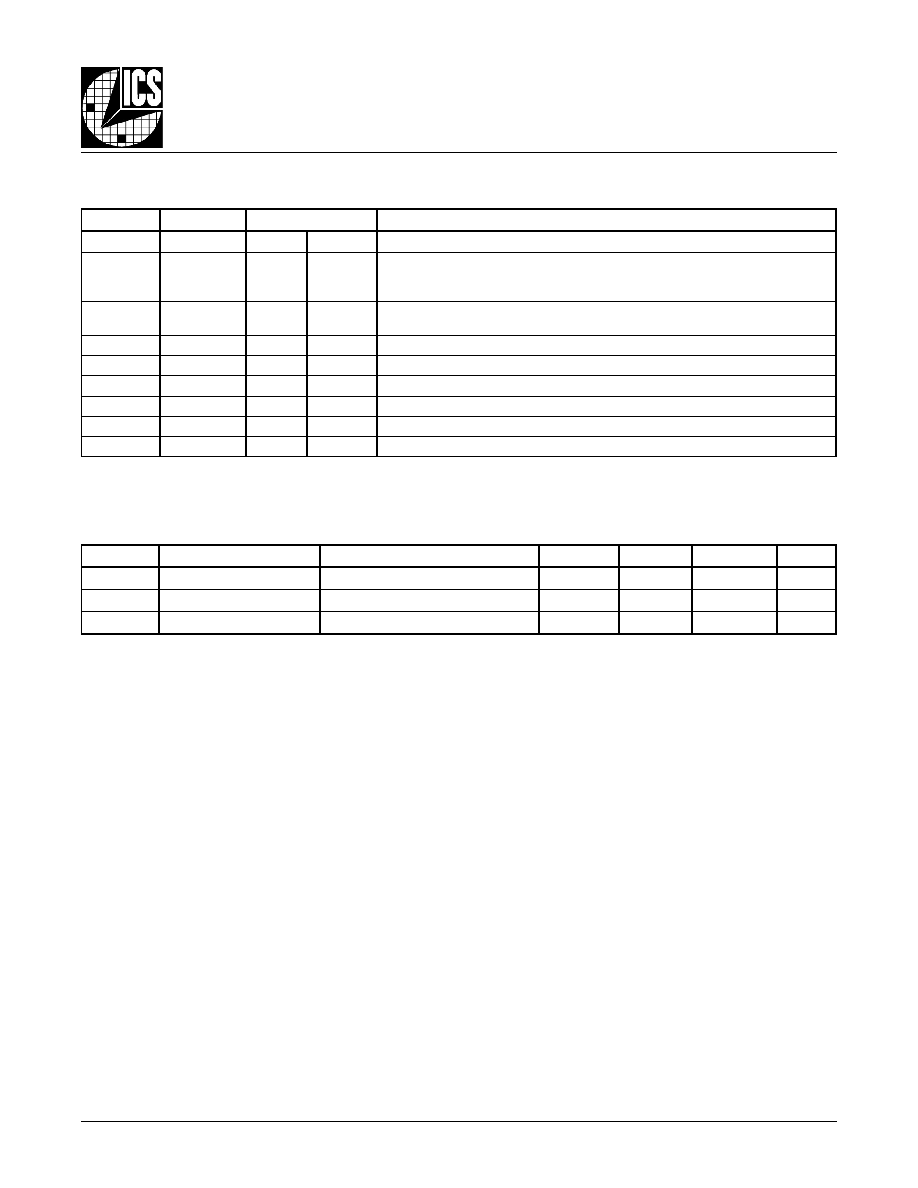
- Absolute Maximum Ratings
- Power Supply DC Characteristics
- LVCMOS DC Characteristics
- LVPECL DC Characteristics
- AC Characteristics
- Additive Phase Jitter
- Parameter Measurement Information
- 3.3V Output Load AC Test Circuit Diagram
- Part-to-Part Skew Diagram
- Output Skew Diagram
- Output Rise/Fall Time Diagram
- Propagation Delay Diagram
- Output Duty Cycle/Pulse Width/Period Diagram
- Application Information
- Termination for LVPECL Outputs
- Schematic Example
- Power Considerations
- Power Dissipation
- Junction Temperature
- Thermal Resistance
- Calculations & Equations
- LVPECL Driver Circuit & Termination Diagram
- Reliability Information
- Transistor Count
- Package Outline
- Package Dimensions
- Ordering Information

8535AG-21
www.icst.com/products/hiperclocks.html
REV. A OCTOBER 20, 2004
1
Integrated
Circuit
Systems, Inc.
ICS8535-21
L
OW
S
KEW
, 1-
TO
-2
LVCMOS/LVTTL-
TO
-3.3V LVPECL F
ANOUT
B
UFFER
G
ENERAL
D
ESCRIPTION
The ICS8535-21 is a low skew, high performance
1-to-2 LVCMOS/LVTTL-to-3.3V LVPECL fanout
buffer and a member of the HiPerClockSTM fam-
ily of High Performance Clock Solutions from
ICS. The ICS8535-21 has two single-ended clock
inputs. The single-ended clock input accepts LVCMOS or
LVTTL input levels and translate them to 3.3V LVPECL lev-
els. The clock enable is internally synchronized to eliminate
runt clock pulses on the output during asynchronous asser-
tion/deassertion of the clock enable pin.
Guaranteed output and part-to-part skew characteristics
make the ICS8535-21 ideal for those applications demand-
ing well defined performance and repeatability.
F
EATURES
∑ 2 differential 3.3V LVPECL outputs
∑ Selectable CLK0 or CLK1 inputs for redundant
and multiple frequency fanout applications
∑ CLK0 or CLK1 can accept the following input levels:
LVCMOS or LVTTL
∑ Maximum output frequency: 266MHz
∑ Translates LVCMOS and LVTTL levels to
3.3V LVPECL levels
∑ Output skew: 20ps (maximum)
∑ Part-to-part skew: 300ps (maximum)
∑ Propagation delay: 1.6ns (maximum)
∑ Additive phase jitter, RMS: 0.03ps (typical)
∑ 3.3V operating supply
∑ 0∞C to 70∞C ambient operating temperature
∑ Industrial temperature information available upon request
B
LOCK
D
IAGRAM
P
IN
A
SSIGNMENT
HiPerClockSTM
ICS
ICS8535-21
14-Lead TSSOP
4.4mm x 5.0mm x 0.92mm body package
G Package
Top View
CLK0
CLK1
Q0
nQ0
Q1
nQ1
0
1
CLK_EN
CLK_SEL
D
Q
LE
V
EE
CLK_EN
CLK_SEL
CLK0
V
EE
CLK1
V
CC
1
2
3
4
5
6
7
14
13
12
11
10
9
8
V
CC
Q0
nQ0
nc
Q1
nQ1
V
CC
8535AG-21
www.icst.com/products/hiperclocks.html
REV. A OCTOBER 20, 2004
2
Integrated
Circuit
Systems, Inc.
ICS8535-21
L
OW
S
KEW
, 1-
TO
-2
LVCMOS/LVTTL-
TO
-3.3V LVPECL F
ANOUT
B
UFFER
T
ABLE
2. P
IN
C
HARACTERISTICS
T
ABLE
1. P
IN
D
ESCRIPTIONS
l
o
b
m
y
S
r
e
t
e
m
a
r
a
P
s
n
o
i
t
i
d
n
o
C
t
s
e
T
m
u
m
i
n
i
M
l
a
c
i
p
y
T
m
u
m
i
x
a
M
s
t
i
n
U
C
N
I
e
c
n
a
t
i
c
a
p
a
C
t
u
p
n
I
4
F
p
R
P
U
L
L
U
P
r
o
t
s
i
s
e
R
p
u
ll
u
P
t
u
p
n
I
1
5
K
R
N
W
O
D
L
L
U
P
r
o
t
s
i
s
e
R
n
w
o
d
ll
u
P
t
u
p
n
I
1
5
K
r
e
b
m
u
N
e
m
a
N
e
p
y
T
n
o
i
t
p
i
r
c
s
e
D
5
,
1
V
E
E
r
e
w
o
P
.
s
n
i
p
y
l
p
p
u
s
e
v
i
t
a
g
e
N
2
N
E
_
K
L
C
t
u
p
n
I
p
u
ll
u
P
.
t
u
p
n
i
k
c
o
l
c
w
o
ll
o
f
s
t
u
p
t
u
o
k
c
o
l
c
,
H
G
I
H
n
e
h
W
.
e
l
b
a
n
e
k
c
o
l
c
g
n
i
z
i
n
o
r
h
c
n
y
S
.
h
g
i
h
d
e
c
r
o
f
e
r
a
s
t
u
p
t
u
o
Q
n
,
w
o
l
d
e
c
r
o
f
e
r
a
s
t
u
p
t
u
o
Q
,
W
O
L
n
e
h
W
.
s
l
e
v
e
l
e
c
a
f
r
e
t
n
i
L
T
T
V
L
/
S
O
M
C
V
L
3
L
E
S
_
K
L
C
t
u
p
n
I
n
w
o
d
ll
u
P
.
t
u
p
n
i
1
K
L
C
s
t
c
e
l
e
s
,
H
G
I
H
n
e
h
W
.
t
u
p
n
i
t
c
e
l
e
s
k
c
o
l
C
.
s
l
e
v
e
l
e
c
a
f
r
e
t
n
i
L
T
T
V
L
/
S
O
M
C
V
L
.
t
u
p
n
i
0
K
L
C
s
t
c
e
l
e
s
,
W
O
L
n
e
h
W
4
0
K
L
C
t
u
p
n
I
n
w
o
d
ll
u
P
.
t
u
p
n
i
k
c
o
l
c
L
T
T
V
L
/
S
O
M
C
V
L
6
1
K
L
C
t
u
p
n
I
n
w
o
d
ll
u
P
.
t
u
p
n
i
k
c
o
l
c
L
T
T
V
L
/
S
O
M
C
V
L
4
1
,
8
,
7
V
C
C
r
e
w
o
P
.
s
n
i
p
y
l
p
p
u
s
e
v
i
t
i
s
o
P
0
1
,
9
1
Q
,
1
Q
n
t
u
p
t
u
O
.
s
l
e
v
e
l
e
c
a
f
r
e
t
n
i
L
C
E
P
V
L
.
r
i
a
p
t
u
p
t
u
o
l
a
i
t
n
e
r
e
f
f
i
D
1
1
c
n
d
e
s
u
n
U
.
t
c
e
n
n
o
c
o
N
3
1
,
2
1
0
Q
,
0
Q
n
t
u
p
t
u
O
.
s
l
e
v
e
l
e
c
a
f
r
e
t
n
i
L
C
E
P
V
L
.
r
i
a
p
t
u
p
t
u
o
l
a
i
t
n
e
r
e
f
f
i
D
:
E
T
O
N
p
u
ll
u
P
d
n
a
n
w
o
d
ll
u
P
.
s
e
u
l
a
v
l
a
c
i
p
y
t
r
o
f
,
s
c
i
t
s
i
r
e
t
c
a
r
a
h
C
n
i
P
,
2
e
l
b
a
T
e
e
S
.
s
r
o
t
s
i
s
e
r
t
u
p
n
i
l
a
n
r
e
t
n
i
o
t
r
e
f
e
r

8535AG-21
www.icst.com/products/hiperclocks.html
REV. A OCTOBER 20, 2004
3
Integrated
Circuit
Systems, Inc.
ICS8535-21
L
OW
S
KEW
, 1-
TO
-2
LVCMOS/LVTTL-
TO
-3.3V LVPECL F
ANOUT
B
UFFER
T
ABLE
3A. C
ONTROL
I
NPUT
F
UNCTION
T
ABLE
T
ABLE
3B. C
LOCK
I
NPUT
F
UNCTION
T
ABLE
s
t
u
p
n
I
s
t
u
p
t
u
O
1
K
L
C
r
o
0
K
L
C
1
Q
,
0
Q
1
Q
n
,
0
Q
n
0
W
O
L
H
G
I
H
1
H
G
I
H
W
O
L
s
t
u
p
n
I
s
t
u
p
t
u
O
N
E
_
K
L
C
L
E
S
_
K
L
C
e
c
r
u
o
S
d
e
t
c
e
l
e
S
1
Q
,
0
Q
1
Q
n
,
0
Q
n
0
0
0
K
L
C
W
O
L
;
d
e
l
b
a
s
i
D
H
G
I
H
;
d
e
l
b
a
s
i
D
0
1
1
K
L
C
W
O
L
;
d
e
l
b
a
s
i
D
H
G
I
H
;
d
e
l
b
a
s
i
D
1
0
0
K
L
C
d
e
l
b
a
n
E
d
e
l
b
a
n
E
1
1
1
K
L
C
d
e
l
b
a
n
E
d
e
l
b
a
n
E
e
g
d
e
k
c
o
l
c
t
u
p
n
i
g
n
il
l
a
f
d
n
a
g
n
i
s
i
r
a
g
n
i
w
o
ll
o
f
d
e
l
b
a
n
e
r
o
d
e
l
b
a
s
i
d
e
r
a
s
t
u
p
t
u
o
k
c
o
l
c
e
h
t
,
s
e
h
c
t
i
w
s
N
E
_
K
L
C
r
e
t
f
A
n
i
w
o
h
s
s
a
.
1
e
r
u
g
i
F
.
B
3
e
l
b
a
T
n
i
d
e
b
i
r
c
s
e
d
s
a
s
t
u
p
n
i
1
K
L
C
d
n
a
0
K
L
C
e
h
t
f
o
n
o
i
t
c
n
u
f
a
e
r
a
s
t
u
p
t
u
o
e
h
t
f
o
e
t
a
t
s
e
h
t
,
e
d
o
m
e
v
i
t
c
a
e
h
t
n
I
F
IGURE
1. CLK_EN T
IMING
D
IAGRAM
Enabled
Disabled
CLK0, CLK1
CLK_EN
nQ0, nQ1
Q0, Q1

8535AG-21
www.icst.com/products/hiperclocks.html
REV. A OCTOBER 20, 2004
4
Integrated
Circuit
Systems, Inc.
ICS8535-21
L
OW
S
KEW
, 1-
TO
-2
LVCMOS/LVTTL-
TO
-3.3V LVPECL F
ANOUT
B
UFFER
T
ABLE
4B. LVCMOS / LVTTL DC C
HARACTERISTICS
,
V
CC
= 3.3V±5%, T
A
= 0∞C
TO
70∞C
T
ABLE
4C. LVPECL DC C
HARACTERISTICS
,
V
CC
= 3.3V±5%, T
A
= 0∞C
TO
70∞C
T
ABLE
4A. P
OWER
S
UPPLY
DC C
HARACTERISTICS
,
V
CC
= 3.3V±5%, T
A
= 0∞C
TO
70∞C
l
o
b
m
y
S
r
e
t
e
m
a
r
a
P
s
n
o
i
t
i
d
n
o
C
t
s
e
T
m
u
m
i
n
i
M
l
a
c
i
p
y
T
m
u
m
i
x
a
M
s
t
i
n
U
V
C
C
e
g
a
t
l
o
V
y
l
p
p
u
S
e
v
i
t
i
s
o
P
5
3
1
.
3
3
.
3
5
6
4
.
3
V
I
E
E
t
n
e
r
r
u
C
y
l
p
p
u
S
r
e
w
o
P
0
5
A
m
NOTE: Stresses beyond those listed under Absolute
Maximum Ratings may cause permanent damage to the
device. These ratings are stress specifications only. Functional
operation of product at these conditions or any conditions
beyond those listed in the
DC Characteristics or AC Charac-
teristics is not implied. Exposure to absolute maximum rating
conditions for extended periods may affect product reliability.
l
o
b
m
y
S
r
e
t
e
m
a
r
a
P
s
n
o
i
t
i
d
n
o
C
t
s
e
T
m
u
m
i
n
i
M
l
a
c
i
p
y
T
m
u
m
i
x
a
M
s
t
i
n
U
V
H
I
e
g
a
t
l
o
V
h
g
i
H
t
u
p
n
I
1
K
L
C
,
0
K
L
C
2
V
C
C
3
.
0
+
V
L
E
S
_
K
L
C
,
N
E
_
K
L
C
2
V
C
C
3
.
0
+
V
V
L
I
e
g
a
t
l
o
V
w
o
L
t
u
p
n
I
1
K
L
C
,
0
K
L
C
3
.
0
-
3
.
1
V
L
E
S
_
K
L
C
,
N
E
_
K
L
C
3
.
0
-
8
.
0
V
I
H
I
t
n
e
r
r
u
C
h
g
i
H
t
u
p
n
I
L
E
S
_
K
L
C
,
1
K
L
C
,
0
K
L
C
V
N
I
V
=
C
C
V
5
6
4
.
3
=
0
5
1
A
µ
N
E
_
K
L
C
V
N
I
V
=
C
C
V
5
6
4
.
3
=
5
A
µ
I
L
I
t
n
e
r
r
u
C
w
o
L
t
u
p
n
I
L
E
S
_
K
L
C
,
1
K
L
C
,
0
K
L
C
V
N
I
V
,
V
0
=
C
C
V
5
6
4
.
3
=
5
-
A
µ
N
E
_
K
L
C
V
N
I
V
,
V
0
=
C
C
V
5
6
4
.
3
=
0
5
1
-
A
µ
l
o
b
m
y
S
r
e
t
e
m
a
r
a
P
s
n
o
i
t
i
d
n
o
C
t
s
e
T
m
u
m
i
n
i
M
l
a
c
i
p
y
T
m
u
m
i
x
a
M
s
t
i
n
U
V
H
O
1
E
T
O
N
;
e
g
a
t
l
o
V
h
g
i
H
t
u
p
t
u
O
V
C
C
4
.
1
-
V
C
C
9
.
0
-
V
V
L
O
1
E
T
O
N
;
e
g
a
t
l
o
V
w
o
L
t
u
p
t
u
O
V
C
C
0
.
2
-
V
C
C
7
.
1
-
V
V
G
N
I
W
S
g
n
i
w
S
e
g
a
t
l
o
V
t
u
p
t
u
O
k
a
e
P
-
o
t
-
k
a
e
P
6
.
0
0
.
1
V
0
5
h
t
i
w
d
e
t
a
n
i
m
r
e
t
s
t
u
p
t
u
O
:
1
E
T
O
N
V
o
t
C
C
.
V
2
-
A
BSOLUTE
M
AXIMUM
R
ATINGS
Supply Voltage, V
CC
4.6V
Inputs, V
I
-0.5V to V
CC
+ 0.5V
Outputs, I
O
Continuous Current
50mA
Surge Current
100mA
Package Thermal Impedance,
JA
93.2∞C/W (0 lfpm)
Storage Temperature, T
STG
-65∞C to 150∞C

8535AG-21
www.icst.com/products/hiperclocks.html
REV. A OCTOBER 20, 2004
5
Integrated
Circuit
Systems, Inc.
ICS8535-21
L
OW
S
KEW
, 1-
TO
-2
LVCMOS/LVTTL-
TO
-3.3V LVPECL F
ANOUT
B
UFFER
T
ABLE
5. AC C
HARACTERISTICS
,
V
CC
= 3.3V±5%, T
A
= 0∞C
TO
70∞C
l
o
b
m
y
S
r
e
t
e
m
a
r
a
P
s
n
o
i
t
i
d
n
o
C
t
s
e
T
m
u
m
i
n
i
M
l
a
c
i
p
y
T
m
u
m
i
x
a
M
s
t
i
n
U
f
X
A
M
y
c
n
e
u
q
e
r
F
t
u
p
t
u
O
6
6
2
z
H
M
t
D
P
1
E
T
O
N
;
y
a
l
e
D
n
o
i
t
a
g
a
p
o
r
P
z
H
M
6
6
2
0
.
1
6
.
1
s
n
t
)
o
(
k
s
5
,
2
E
T
O
N
;
w
e
k
S
t
u
p
t
u
O
0
2
s
p
t
)
p
p
(
k
s
5
,
3
E
T
O
N
;
w
e
k
S
t
r
a
P
-
o
t
-
t
r
a
P
0
0
3
s
p
t t
ij
;
S
M
R
,
r
e
t
t
i
J
e
s
a
h
P
e
v
i
t
i
d
d
A
r
e
f
f
u
B
r
e
t
t
i
J
e
s
a
h
P
e
v
i
t
i
d
d
A
o
t
r
e
f
e
r
4
E
T
O
N
,
n
o
i
t
c
e
S
n
o
i
t
a
r
g
e
t
n
I
@
z
H
M
5
2
.
6
5
1
z
H
M
0
2
-
z
H
K
2
1
:
e
g
n
a
R
3
0
.
0
s
p
t
R
t
/
F
e
m
i
T
ll
a
F
/
e
s
i
R
t
u
p
t
u
O
z
H
M
0
5
@
%
0
8
o
t
%
0
2
0
0
3
0
0
6
s
p
c
d
o
e
l
c
y
C
y
t
u
D
t
u
p
t
u
O
z
H
M
0
0
2
5
4
5
5
%
t
a
d
e
r
u
s
a
e
m
s
r
e
t
e
m
a
r
a
p
ll
A
z
H
M
6
6
2
.
e
s
i
w
r
e
h
t
o
d
e
t
o
n
s
s
e
l
n
u
.
r
e
t
t
ij
d
d
a
t
o
n
s
e
o
d
t
r
a
p
e
h
T
.
t
u
p
t
u
o
e
h
t
n
o
r
e
t
t
ij
e
h
t
l
a
u
q
e
ll
i
w
t
u
p
n
i
e
h
t
n
o
r
e
t
t
ij
e
l
c
y
c
-
o
t
-
e
l
c
y
c
e
h
T
V
e
h
t
m
o
r
f
d
e
r
u
s
a
e
M
:
1
E
T
O
N
C
C
.
t
n
i
o
p
g
n
i
s
s
o
r
c
t
u
p
t
u
o
l
a
i
t
n
e
r
e
f
f
i
d
e
h
t
o
t
t
u
p
n
i
e
h
t
f
o
2
/
.
s
n
o
i
t
i
d
n
o
c
d
a
o
l
l
a
u
q
e
h
t
i
w
d
n
a
e
g
a
t
l
o
v
y
l
p
p
u
s
e
m
a
s
e
h
t
t
a
s
t
u
p
t
u
o
n
e
e
w
t
e
b
w
e
k
s
s
a
d
e
n
i
f
e
D
:
2
E
T
O
N
.
s
t
n
i
o
p
s
s
o
r
c
l
a
i
t
n
e
r
e
f
f
i
d
t
u
p
t
u
o
e
h
t
t
a
d
e
r
u
s
a
e
M
s
e
g
a
t
l
o
v
y
l
p
p
u
s
e
m
a
s
e
h
t
t
a
g
n
i
t
a
r
e
p
o
s
e
c
i
v
e
d
t
n
e
r
e
f
f
i
d
n
o
s
t
u
p
t
u
o
n
e
e
w
t
e
b
w
e
k
s
s
a
d
e
n
i
f
e
D
:
3
E
T
O
N
d
e
r
u
s
a
e
m
e
r
a
s
t
u
p
t
u
o
e
h
t
,
e
c
i
v
e
d
h
c
a
e
n
o
s
t
u
p
n
i
f
o
e
p
y
t
e
m
a
s
e
h
t
g
n
i
s
U
.
s
n
o
i
t
i
d
n
o
c
d
a
o
l
l
a
u
q
e
h
t
i
w
d
n
a
.
s
t
n
i
o
p
s
s
o
r
c
l
a
i
t
n
e
r
e
f
f
i
d
e
h
t
t
a
.
k
c
o
l
c
t
u
p
n
i
e
n
o
y
l
n
o
g
n
i
v
i
r
D
:
4
E
T
O
N
.
5
6
d
r
a
d
n
a
t
S
C
E
D
E
J
h
t
i
w
e
c
n
a
d
r
o
c
c
a
n
i
d
e
n
i
f
e
d
s
i
r
e
t
e
m
a
r
a
p
s
i
h
T
:
5
E
T
O
N

8535AG-21
www.icst.com/products/hiperclocks.html
REV. A OCTOBER 20, 2004
6
Integrated
Circuit
Systems, Inc.
ICS8535-21
L
OW
S
KEW
, 1-
TO
-2
LVCMOS/LVTTL-
TO
-3.3V LVPECL F
ANOUT
B
UFFER
A
DDITIVE
P
HASE
J
ITTER
Input/Output Additive Phase Jitter,
Integration Range: 12KHz - 20MHz at
156.25MHz = 0.03ps (typical)
0
-10
-20
-30
-40
-50
-60
-70
-80
-90
-100
-110
-120
-130
-140
-150
-160
-170
-180
-190
1k
10k
100k
1M
10M
100M
The spectral purity in a band at a specific offset from the fun-
damental compared to the power of the fundamental is called
the
dBc Phase Noise. This value is normally expressed using
a Phase noise plot and is most often the specified plot in many
applications. Phase noise is defined as the ratio of the noise
power present in a 1Hz band at a specified offset from the
fundamental frequency to the power value of the fundamental.
This ratio is expressed in decibels (dBm) or a ratio of the power
As with most timing specifications, phase noise measurements
have issues. The primary issue relates to the limitations of the
equipment. Often the noise floor of the equipment is higher
than the noise floor of the device. This is illustrated above. The
in the 1Hz band to the power in the fundamental. When the
required offset is specified, the phase noise is called a
dBc
value, which simply means dBm at a specified offset from the
fundamental. By investigating jitter in the frequency domain,
we get a better understanding of its effects on the desired ap-
plication over the entire time record of the signal. It is math-
ematically possible to calculate an expected bit error rate given
a phase noise plot.
device meets the noise floor of what is shown, but can actually
be lower. The phase noise is dependant on the input source
and measurement equipment.
O
FFSET
F
ROM
C
ARRIER
F
REQUENCY
(H
Z
)
SSB P
HASE
N
OISE
dB
c
/
H
Z

8535AG-21
www.icst.com/products/hiperclocks.html
REV. A OCTOBER 20, 2004
7
Integrated
Circuit
Systems, Inc.
ICS8535-21
L
OW
S
KEW
, 1-
TO
-2
LVCMOS/LVTTL-
TO
-3.3V LVPECL F
ANOUT
B
UFFER
P
ARAMETER
M
EASUREMENT
I
NFORMATION
O
UTPUT
R
ISE
/F
ALL
T
IME
P
ROPAGATION
D
ELAY
O
UTPUT
D
UTY
C
YCLE
/P
ULSE
W
IDTH
/P
ERIOD
O
UTPUT
S
KEW
3.3V O
UTPUT
L
OAD
AC T
EST
C
IRCUIT
SCOPE
Qx
nQx
LVPECL
2V
-1.3V ± 0.165V
t
sk(o)
nQx
Qx
nQy
Qy
Clock
Outputs
20%
80%
80%
20%
t
R
t
F
V
SW I N G
Pulse Width
t
PERIOD
t
PW
t
PERIOD
odc =
Q0, Q1
nQ0, nQ1
t
PD
CLK0,
CLK1
tsk(pp)
nQx
Qx
nQy
Qy
PART 1
PART 2
P
ART
-
TO
-P
ART
S
KEW
Q0, Q1
nQ0, nQ1
V
CC
V
EE

8535AG-21
www.icst.com/products/hiperclocks.html
REV. A OCTOBER 20, 2004
8
Integrated
Circuit
Systems, Inc.
ICS8535-21
L
OW
S
KEW
, 1-
TO
-2
LVCMOS/LVTTL-
TO
-3.3V LVPECL F
ANOUT
B
UFFER
A
PPLICATION
I
NFORMATION
V
CC
- 2V
50
50
RTT
Z
o
= 50
Z
o
= 50
FOUT
FIN
RTT =
Z
o
1
((V
OH
+ V
OL
) / (V
CC
≠ 2)) ≠ 2
3.3V
125
125
84
84
Z
o
= 50
Z
o
= 50
FOUT
FIN
The clock layout topology shown below is a typical termina-
tion for LVPECL outputs. The two different layouts mentioned
are recommended only as guidelines.
FOUT and nFOUT are low impedance follower outputs that
generate ECL/LVPECL compatible outputs. Therefore, termi-
nating resistors (DC current path to ground) or current sources
must be used for functionality. These outputs are designed to
drive 50
transmission lines. Matched impedance techniques
should be used to maximize operating frequency and minimize
signal distortion.
Figures 2A and 2B show two different layouts
which are recommended only as guidelines. Other suitable
clock layouts may exist and it would be recommended that the
board designers simulate to guarantee compatibility across all
printed circuit and clock component process variations.
F
IGURE
2B. LVPECL O
UTPUT
T
ERMINATION
F
IGURE
2A. LVPECL O
UTPUT
T
ERMINATION
T
ERMINATION
FOR
LVPECL O
UTPUTS

8535AG-21
www.icst.com/products/hiperclocks.html
REV. A OCTOBER 20, 2004
9
Integrated
Circuit
Systems, Inc.
ICS8535-21
L
OW
S
KEW
, 1-
TO
-2
LVCMOS/LVTTL-
TO
-3.3V LVPECL F
ANOUT
B
UFFER
S
CHEMATIC
E
XAMPLE
Figure 3 shows a schematic example of the ICS8535-21. The
decoupling capacitors should be physically located near the
power pin. For ICS8535-21, the unused clock outputs can be
left floating.
F
IGURE
3. ICS8535-21 LVPECL B
UFFER
S
CHEMATIC
E
XAMPLE
VCC
R5
82.5
R3
50
+
-
CLK0
C1
10uf
Optional Termination
R4
133
(U1-14)
R2
50
Zo = 50
R7
82.5
Zo = 50
CLK1
C2
.1uF
Zo = 50
(U1-8)
Vcco = 3.3V
VCC = 3.3V
R1
50
CLK_EN
(U1-7)
Zo = 50
C4
.1uF
R6
133
CLK_SEL
+
-
U2
8535-21
1
2
3
4
5
6
11
8
9
10
12
14
13
7
VEE
CLK_EN
CLK_SEL
CLK0
VEE
CLK1
nc
VCC
nQ1
Q1
nQ0
VCC
Q0
VCC
C3
.1uF

8535AG-21
www.icst.com/products/hiperclocks.html
REV. A OCTOBER 20, 2004
10
Integrated
Circuit
Systems, Inc.
ICS8535-21
L
OW
S
KEW
, 1-
TO
-2
LVCMOS/LVTTL-
TO
-3.3V LVPECL F
ANOUT
B
UFFER
P
OWER
C
ONSIDERATIONS
This section provides information on power dissipation and junction temperature for the ICS8535-21.
Equations and example calculations are also provided.
1. Power Dissipation.
The total power dissipation for the ICS8535-21 is the sum of the core power plus the power dissipated in the load(s).
The following is the power dissipation for V
CC
= 3.3V + 5% = 3.465V, which gives worst case results.
NOTE: Please refer to Section 3 for details on calculating power dissipated in the load.
∑
Power (core)
MAX
= V
CC_MAX
* I
EE_MAX
= 3.465V * 50mA = 173.25mW
∑
Power (outputs)
MAX
= 30mW/Loaded Output pair
If all outputs are loaded, the total power is 2 x 30mW = 60mW
Total Power
_MAX
(3.465V, with all outputs switching) = 173.25mW + 60mW = 233.25mW
2. Junction Temperature.
Junction temperature, Tj, is the temperature at the junction of the bond wire and bond pad and directly affects the reliability of
the device. The maximum recommended junction temperature for HiPerClockS
TM
devices is 125∞C.
The equation for Tj is as follows: Tj =
JA
* Pd_total + T
A
Tj = Junction Temperature
JA
= Junction-to-Ambient Thermal Resistance
Pd_total = Total Device Power Dissipation (example calculation is in section 1 above)
T
A
= Ambient Temperature
In order to calculate junction temperature, the appropriate junction-to-ambient thermal resistance
JA
must be used. Assuming a
moderate air low of 200 linear feet per minute and a multi-layer board, the appropriate value is 85.5∞C/W per Table 6 below.
Therefore, Tj for an ambient temperature of 70∞C with all outputs switching is:
70∞C + 0.233W * 85.5∞C/W = 90∞C. This is well below the limit of 125∞C.
This calculation is only an example, and the Tj will obviously vary depending on the number of outputs that are loaded, supply
voltage, air flow, and the type of board (single layer or multi-layer).
JA
by Velocity (Linear Feet per Minute)
T
ABLE
6. T
HERMAL
R
ESISTANCE
JA
FOR
14-
PIN
TSSOP, F
ORCED
C
ONVECTION
0
200
500
Single-Layer PCB, JEDEC Standard Test Boards
146.4∞C/W
125.2∞C/W
112.1∞C/W
Multi-Layer PCB, JEDEC Standard Test Boards
93.2∞C/W
85.5∞C/W
81.2∞C/W
NOTE: Most modern PCB designs use multi-layered boards. The data in the second row pertains to most designs.

8535AG-21
www.icst.com/products/hiperclocks.html
REV. A OCTOBER 20, 2004
11
Integrated
Circuit
Systems, Inc.
ICS8535-21
L
OW
S
KEW
, 1-
TO
-2
LVCMOS/LVTTL-
TO
-3.3V LVPECL F
ANOUT
B
UFFER
3. Calculations and Equations.
The purpose of this section is to derive the power dissipated into the load.
LVPECL output driver circuit and termination are shown in
Figure 4.
T
o calculate worst case power dissipation into the load, use the following equations which assume a 50
load, and a
termination voltage of V
CC
- 2V.
∑
For logic high, V
OUT
= V
OH_MAX
= V
CC_MAX
≠ 0.9V
(V
CC_MAX
- V
OH_MAX
) = 0.9V
∑
For logic low, V
OUT
= V
OL_MAX
= V
CC_MAX
≠ 1.7V
(V
CC_MAX
- V
OL_MAX
) = 1.7V
Pd_H is power dissipation when the output drives high.
Pd_L is the power dissipation when the output drives low.
Pd_H = [(V
OH_MAX
≠ (V
CC_MAX
- 2V))/R
L
] * (V
CC_MAX
- V
OH_MAX
) = [(2V - (V
CC_MAX
- V
OH_MAX
))/R
L
] * (V
CC_MAX
- V
OH_MAX
) =
[(2V - 0.9V)/50
] * 0.9V = 19.8mW
Pd_L = [(V
OL_MAX
≠ (V
CC_MAX
- 2V))/R
L
] * (V
CC_MAX
- V
OL_MAX
) = [(2V - (V
CC_MAX
- V
OL_MAX
))/R
L
] * (V
CC_MAX
- V
OL_MAX
) =
[(2V - 1.7V)/50
] * 1.7V = 10.2mW
Total Power Dissipation per output pair = Pd_H + Pd_L = 30mW
F
IGURE
4. LVPECL D
RIVER
C
IRCUIT
AND
T
ERMINATION
Q1
V
OUT
V
CC
RL
50
V
CC
- 2V

8535AG-21
www.icst.com/products/hiperclocks.html
REV. A OCTOBER 20, 2004
12
Integrated
Circuit
Systems, Inc.
ICS8535-21
L
OW
S
KEW
, 1-
TO
-2
LVCMOS/LVTTL-
TO
-3.3V LVPECL F
ANOUT
B
UFFER
R
ELIABILITY
I
NFORMATION
T
RANSISTOR
C
OUNT
The transistor count for ICS8535-21 is: 412
T
ABLE
7.
JA
VS
. A
IR
F
LOW
T
ABLE
FOR
14 L
EAD
TSSOP
JA
by Velocity (Linear Feet per Minute)
0
200
500
Single-Layer PCB, JEDEC Standard Test Boards
146.4∞C/W
125.2∞C/W
112.1∞C/W
Multi-Layer PCB, JEDEC Standard Test Boards
93.2∞C/W
85.5∞C/W
81.2∞C/W
NOTE: Most modern PCB designs use multi-layered boards. The data in the second row pertains to most designs.

8535AG-21
www.icst.com/products/hiperclocks.html
REV. A OCTOBER 20, 2004
13
Integrated
Circuit
Systems, Inc.
ICS8535-21
L
OW
S
KEW
, 1-
TO
-2
LVCMOS/LVTTL-
TO
-3.3V LVPECL F
ANOUT
B
UFFER
P
ACKAGE
O
UTLINE
- G S
UFFIX
FOR
14 L
EAD
TSSOP
T
ABLE
8. P
ACKAGE
D
IMENSIONS
R
EFERENCE
D
OCUMENT
: JEDEC P
UBLICATION
95, MO-153
L
O
B
M
Y
S
s
r
e
t
e
m
i
l
l
i
M
m
u
m
i
n
i
M
m
u
m
i
x
a
M
N
4
1
A
-
-
0
2
.
1
1
A
5
0
.
0
5
1
.
0
2
A
0
8
.
0
5
0
.
1
b
9
1
.
0
0
3
.
0
c
9
0
.
0
0
2
.
0
D
0
9
.
4
0
1
.
5
E
C
I
S
A
B
0
4
.
6
1
E
0
3
.
4
0
5
.
4
e
C
I
S
A
B
5
6
.
0
L
5
4
.
0
5
7
.
0
∞
0
∞
8
a
a
a
-
-
0
1
.
0
8535AG-21
www.icst.com/products/hiperclocks.html
REV. A OCTOBER 20, 2004
14
Integrated
Circuit
Systems, Inc.
ICS8535-21
L
OW
S
KEW
, 1-
TO
-2
LVCMOS/LVTTL-
TO
-3.3V LVPECL F
ANOUT
B
UFFER
T
ABLE
9. O
RDERING
I
NFORMATION
<
While the information presented herein has been checked for both accuracy and reliability, Integrated Circuit Systems, Incorporated (ICS) assumes no responsibility for either its use or
for infringement of any patents or other rights of third parties, which would result from its use. No other circuits, patents, or licenses are implied. This product is intended for use in normal
commercial applications. Any other applications such as those requiring extended temperature range, high reliability, or other extraordinary environmental requirements are not recom-
mended without additional processing by ICS. ICS reserves the right to change any circuitry or specifications without notice. ICS does not authorize or warrant any ICS product for use
in life support devices or critical medical instruments.
r
e
b
m
u
N
r
e
d
r
O
/
t
r
a
P
g
n
i
k
r
a
M
e
g
a
k
c
a
P
t
n
u
o
C
e
r
u
t
a
r
e
p
m
e
T
1
2
-
G
A
5
3
5
8
S
C
I
1
2
G
A
5
3
5
8
P
O
S
S
T
d
a
e
l
4
1
e
b
u
t
r
e
p
4
9
C
∞
0
7
o
t
C
∞
0
T
1
2
-
G
A
5
3
5
8
S
C
I
1
2
G
A
5
3
5
8
l
e
e
R
d
n
a
e
p
a
T
n
o
P
O
S
S
T
d
a
e
l
4
1
0
0
5
2
C
∞
0
7
o
t
C
∞
0
The aforementioned trademark, HiPerClockSTM is a trademark of Integrated Circuit Systems, Inc. or its subsidiaries in the United States and/or other countries.