854057AG
www.icst.com/products/hiperclocks.html
REV. A JULY 18, 2005
1
Integrated
Circuit
Systems, Inc.
ICS854057
4:1
OR
2:1 LVDS C
LOCK
M
ULTIPLEXER
WITH
I
NTERNAL
I
NPUT
T
ERMINATION
G
ENERAL
D
ESCRIPTION
The ICS854057 is a 4:1 or 2:1 LVDS Clock Mul-
tiplexer which can operate up to 2GHz and is a
member of the HiPerClockSTM family of High Per-
formance Clock Solutions from ICS. The PCLK,
nPCLK pairs can accept most standard differen-
tial input levels. Internal termination is provided on each dif-
ferential input pair. The ICS854057 operates using a 2.5V sup-
ply voltage. The fully differential architecture and low propa-
gation delay make it ideal for use in high speed multiplexing
applications. The select pins have internal pulldown resistors.
Leaving one input unconnected (pulled to logic low by the in-
ternal resistor) will transform the device into a 2:1 multiplexer.
The SEL1 pin is the most significant bit and the binary num-
ber applied to the select pins will select the same numbered
data input (i.e., 00 selects PCLK0, nPCLK0).
F
EATURES
· High speed differential multiplexer. The device can be
configured as either a 4:1 or 2:1 multiplexer
· Single LVDS output
· 4 selectable PCLK, nPCLK inputs with internal termination
· PCLK, nPCLK pairs can accept the following differential
input levels: LVPECL, LVDS, CML, SSTL
· Output frequency: >2GHz
· Part-to-part skew: 200ps (maximum)
· Propagation delay: 800ps (maximum)
· Additive phase jitter, RMS: 66fs (typical)
· 2.5V operating supply
· -40°C to 85°C ambient operating temperature
· Available in both, Standard and RoHS/Lead-Free compliant
packages
HiPerClockSTM
ICS
00
01
10
11
B
LOCK
D
IAGRAM
P
IN
A
SSIGNMENT
V
DD
PCLK0
VT0
nPCLK0
SEL1
SEL0
PCLK1
VT1
nPCLK1
GND
1
2
3
4
5
6
7
8
9
10
20
19
18
17
16
15
14
13
12
11
V
DD
PCLK3
VT3
nPCLK3
Q
nQ
PCLK2
VT2
nPCLK2
GND
ICS854057
20-Lead TSSOP
4.40mm x 6.50mm x 0.925mm body package
G Package
Top View
VT0
PCLK0
nPCLK0
VT1
PCLK1
nPCLK1
VT2
PCLK2
nPCLK2
VT3
PCLK3
nPCLK3
Q
nQ
50 50
50 50
50 50
50 50
SEL1
SEL0
Pulldown
Pulldown
854057AG
www.icst.com/products/hiperclocks.html
REV. A JULY 18, 2005
3
Integrated
Circuit
Systems, Inc.
ICS854057
4:1
OR
2:1 LVDS C
LOCK
M
ULTIPLEXER
WITH
I
NTERNAL
I
NPUT
T
ERMINATION
T
ABLE
4A. P
OWER
S
UPPLY
DC C
HARACTERISTICS
,
V
DD
= 2.5V ± 5%, T
A
= -40°C
TO
85°C
T
ABLE
4B. LVCMOS / LVTTL DC C
HARACTERISTICS
,
V
DD
= 2.5V ± 5%, T
A
= -40°C
TO
85°C
l
o
b
m
y
S
r
e
t
e
m
a
r
a
P
s
n
o
i
t
i
d
n
o
C
t
s
e
T
m
u
m
i
n
i
M
l
a
c
i
p
y
T
m
u
m
i
x
a
M
s
t
i
n
U
V
D
D
e
g
a
t
l
o
V
y
l
p
p
u
S
e
v
i
t
i
s
o
P
5
7
3
.
2
5
.
2
5
2
6
.
2
V
I
D
D
t
n
e
r
r
u
C
y
l
p
p
u
S
r
e
w
o
P
0
6
A
m
T
ABLE
4C. LVPECL DC C
HARACTERISTICS
,
V
DD
= 2.5V ± 5%, T
A
= -40°C
TO
85°C
l
o
b
m
y
S
r
e
t
e
m
a
r
a
P
s
n
o
i
t
i
d
n
o
C
t
s
e
T
m
u
m
i
n
i
M
l
a
c
i
p
y
T
m
u
m
i
x
a
M
s
t
i
n
U
I
H
I
t
n
e
r
r
u
C
h
g
i
H
t
u
p
n
I
V
D
D
V
=
N
I
V
5
2
6
.
2
=
0
5
1
A
µ
I
L
I
t
n
e
r
r
u
C
w
o
L
t
u
p
n
I
V
D
D
V
,
V
5
2
6
.
2
=
N
I
V
0
=
0
5
1
-
A
µ
V
P
P
e
g
a
t
l
o
V
k
a
e
P
-
o
t
-
k
a
e
P
5
1
.
0
2
.
1
V
V
R
M
C
2
,
1
E
T
O
N
;
e
g
a
t
l
o
V
t
u
p
n
I
e
d
o
M
n
o
m
m
o
C
2
.
1
V
D
D
V
V
s
a
d
e
n
i
f
e
d
s
i
e
g
a
t
l
o
v
t
u
p
n
i
e
d
o
m
n
o
m
m
o
C
:
1
E
T
O
N
H
I
.
V
s
i
x
K
L
C
P
n
,
x
K
L
C
P
r
o
f
e
g
a
t
l
o
v
t
u
p
n
i
m
u
m
i
x
a
m
e
h
t
,
s
n
o
i
t
a
c
il
p
p
a
d
e
d
n
e
e
l
g
n
i
s
r
o
F
:
2
E
T
O
N
D
D
.
V
3
.
0
+
l
o
b
m
y
S
r
e
t
e
m
a
r
a
P
s
n
o
i
t
i
d
n
o
C
t
s
e
T
m
u
m
i
n
i
M
l
a
c
i
p
y
T
m
u
m
i
x
a
M
s
t
i
n
U
V
H
I
e
g
a
t
l
o
V
h
g
i
H
t
u
p
n
I
V
*
7
.
0
D
D
V
D
D
3
.
0
+
V
V
L
I
e
g
a
t
l
o
V
w
o
L
t
u
p
n
I
3
.
0
-
V
*
3
.
0
D
D
V
I
H
I
t
n
e
r
r
u
C
h
g
i
H
t
u
p
n
I
1
L
E
S
,
0
L
E
S
V
D
D
V
=
N
I
V
5
2
6
.
2
=
0
5
1
A
µ
I
L
I
t
n
e
r
r
u
C
w
o
L
t
u
p
n
I
1
L
E
S
,
0
L
E
S
V
D
D
V
,
V
5
2
6
.
2
=
N
I
V
0
=
0
5
1
-
A
µ
A
BSOLUTE
M
AXIMUM
R
ATINGS
Supply Voltage, V
DD
4.6V
Inputs, V
I
-0.5V to V
DD
+ 0.5 V
Outputs, I
O
Continuous Current
10mA
Surge Current
15mA
Package Thermal Impedance,
JA
73.2°C/W (0 lfpm)
Storage Temperature, T
STG
-65°C to 150°C
NOTE: Stresses beyond those listed under Absolute
Maximum Ratings may cause permanent damage to the
device. These ratings are stress specifications only. Functional
operation of product at these conditions or any conditions be-
yond those listed in the
DC Characteristics or AC Character-
istics is not implied. Exposure to absolute maximum rating
conditions for extended periods may affect product reliability.
854057AG
www.icst.com/products/hiperclocks.html
REV. A JULY 18, 2005
5
Integrated
Circuit
Systems, Inc.
ICS854057
4:1
OR
2:1 LVDS C
LOCK
M
ULTIPLEXER
WITH
I
NTERNAL
I
NPUT
T
ERMINATION
A
DDITIVE
P
HASE
J
ITTER
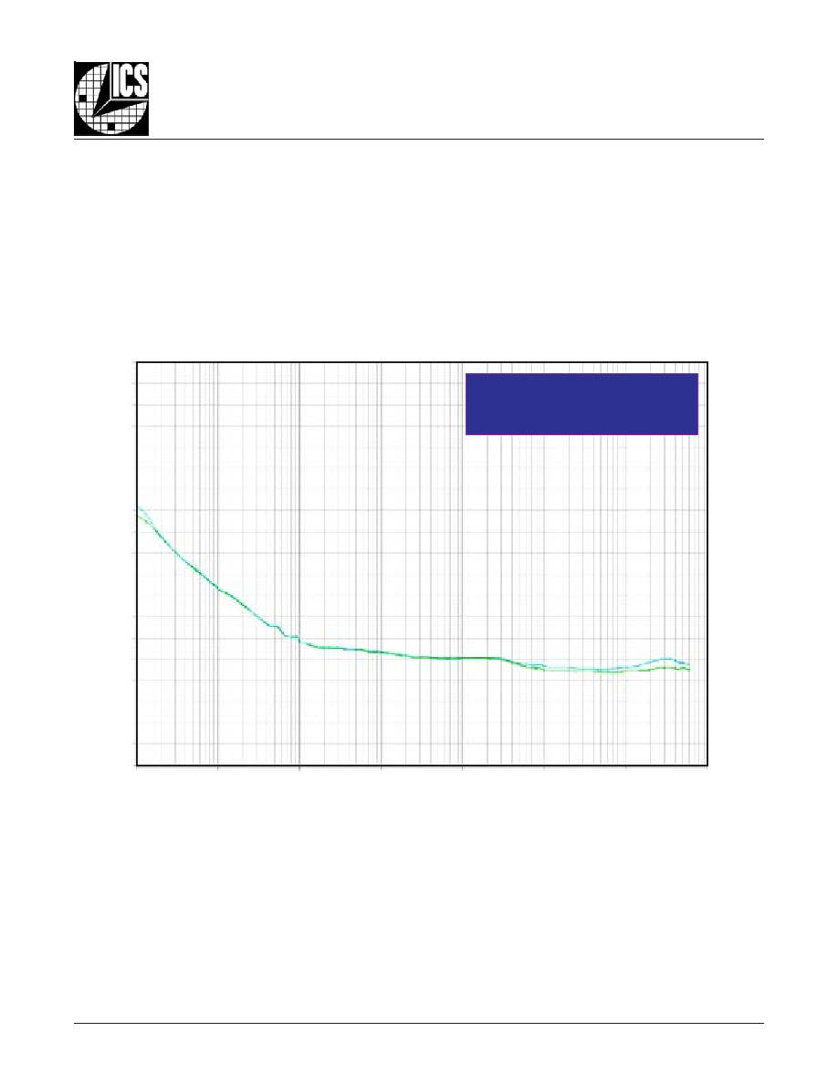
Additive Phase Jitter
@ 622.08MHz
(12kHz to 20MHz)
= 66fs typical
0
-10
-20
-30
-40
-50
-60
-70
-80
-90
-100
-110
-120
-130
-140
-150
-160
-170
-180
-190
100
1k
10k
100k
1M
10M
100M
500M
The spectral purity in a band at a specific offset from the funda-
mental compared to the power of the fundamental is called the
dBc Phase Noise. This value is normally expressed using a
Phase noise plot and is most often the specified plot in many
applications. Phase noise is defined as the ratio of the noise
power present in a 1Hz band at a specified offset from the fun-
damental frequency to the power value of the fundamental. This
ratio is expressed in decibels (dBm) or a ratio of the power in
As with most timing specifications, phase noise measurements
have issues. The primary issue relates to the limitations of the
equipment. Often the noise floor of the equipment is higher than
the noise floor of the device. This is illustrated above. The de-
the 1Hz band to the power in the fundamental. When the re-
quired offset is specified, the phase noise is called a
dBc value,
which simply means dBm at a specified offset from the funda-
mental. By investigating jitter in the frequency domain, we get a
better understanding of its effects on the desired application over
the entire time record of the signal. It is mathematically possible
to calculate an expected bit error rate given a phase noise plot.
vice meets the noise floor of what is shown, but can actually be
lower. The phase noise is dependant on the input source and
measurement equipment.
O
FFSET
F
ROM
C
ARRIER
F
REQUENCY
(H
Z
)
SSB P
HASE
N
OISE
dB
c
/
H
Z