Äîêóìåíòàöèÿ è îïèñàíèÿ www.docs.chipfind.ru
85411AM
www.icst.com/products/hiperclocks.html
REV. B JUNE 16, 2004
1
Integrated
Circuit
Systems, Inc.
ICS85411
L
OW
S
KEW
, 1-
TO
-2
D
IFFERENTIAL
-
TO
-LVDS F
ANOUT
B
UFFER
G
ENERAL
D
ESCRIPTION
The ICS85411 is a low skew, high performance
1-to-2 Differential-to-LVDS Fanout Buffer and a
member of the HiPerClockSTM family of High
Perfor mance Clock Solutions from ICS. The
CLK, nCLK pair can accept most standard differ-
ential input levels.The ICS85411 is characterized to oper-
ate from a 3.3V power supply. Guaranteed output and
par t-to-par t skew character istics make the ICS85411
ideal for those clock distribution applications demand-
ing well defined perfor mance and repeatability.
F
EATURES
· 2 differential LVDS outputs
· 1 differential CLK, nCLK clock input
· CLK, nCLK pair can accept the following differential
input levels: LVPECL, LVDS, LVHSTL, SSTL, HCSL
· Maximum output frequency: 650MHz
· Translates any single ended input signal to
LVDS levels with resistor bias on nCLK input
· Output skew: 20ps (maximum)
· Part-to-part skew: 250ps (maximum)
· Additive phase jitter, RMS: 0.05ps (typical)
· Propagation delay: 2.5 ns (maximum)
· 3.3V operating supply
· 0°C to 70°C ambient operating temperature
· Lead-Free package available
· Industrial temperature information available upon request
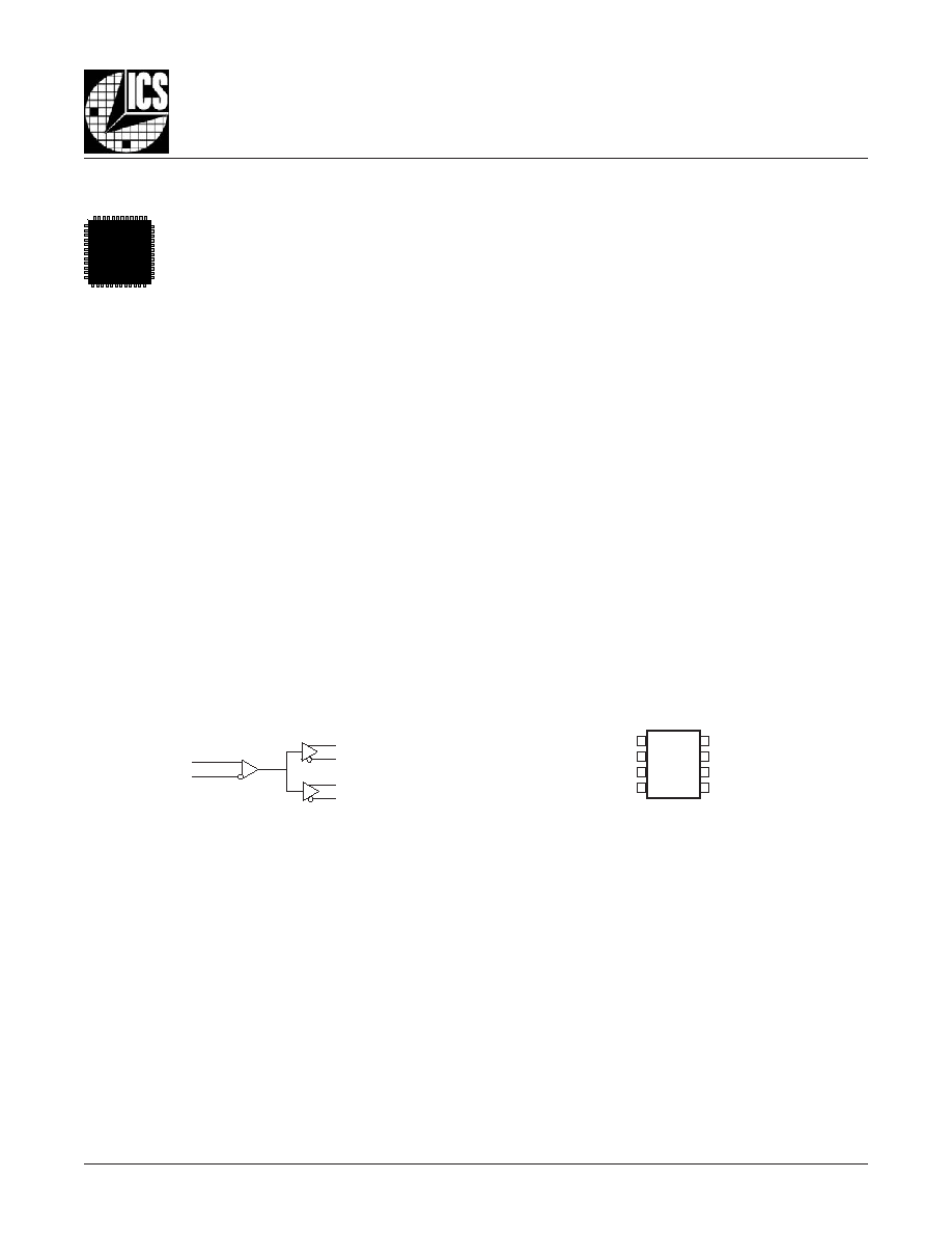
B
LOCK
D
IAGRAM
P
IN
A
SSIGNMENT
ICS85411
8-Lead SOIC
3.90mm x 4.90mm x 1.37mm package body
M Package
Top View
Q0
nQ0
Q1
nQ1
1
2
3
4
HiPerClockSTM
ICS
V
DD
CLK
nCLK
GND
8
7
6
5
Q0
nQ0
Q1
nQ1
CLK
nCLK
85411AM
www.icst.com/products/hiperclocks.html
REV. B JUNE 16, 2004
2
Integrated
Circuit
Systems, Inc.
ICS85411
L
OW
S
KEW
, 1-
TO
-2
D
IFFERENTIAL
-
TO
-LVDS F
ANOUT
B
UFFER
T
ABLE
1. P
IN
D
ESCRIPTIONS
T
ABLE
2. P
IN
C
HARACTERISTICS
r
e
b
m
u
N
e
m
a
N
e
p
y
T
n
o
i
t
p
i
r
c
s
e
D
2
,
1
0
Q
n
,
0
Q
t
u
p
t
u
O
.
s
l
e
v
e
l
e
c
a
f
r
e
t
n
i
S
D
V
L
.
r
i
a
p
t
u
p
t
u
o
l
a
i
t
n
e
r
e
f
f
i
D
4
,
3
1
Q
n
,
1
Q
t
u
p
t
u
O
.
s
l
e
v
e
l
e
c
a
f
r
e
t
n
i
S
D
V
L
.
r
i
a
p
t
u
p
t
u
o
l
a
i
t
n
e
r
e
f
f
i
D
5
D
N
G
r
e
w
o
P
.
d
n
u
o
r
g
y
l
p
p
u
s
r
e
w
o
P
6
K
L
C
n
t
u
p
n
I
n
w
o
d
ll
u
P
.
t
u
p
n
i
k
c
o
l
c
l
a
i
t
n
e
r
e
f
f
i
d
g
n
i
t
r
e
v
n
I
7
K
L
C
t
u
p
n
I
p
u
ll
u
P
.
t
u
p
n
i
k
c
o
l
c
l
a
i
t
n
e
r
e
f
f
i
d
g
n
i
t
r
e
v
n
i
-
n
o
N
8
V
D
D
r
e
w
o
P
.
n
i
p
y
l
p
p
u
s
e
v
i
t
i
s
o
P
:
E
T
O
N
p
u
ll
u
P
d
n
a
n
w
o
d
ll
u
P
.
s
e
u
l
a
v
l
a
c
i
p
y
t
r
o
f
,
s
c
i
t
s
i
r
e
t
c
a
r
a
h
C
n
i
P
,
2
e
l
b
a
T
e
e
S
.
s
r
o
t
s
i
s
e
r
t
u
p
n
i
l
a
n
r
e
t
n
i
o
t
r
e
f
e
r
l
o
b
m
y
S
r
e
t
e
m
a
r
a
P
s
n
o
i
t
i
d
n
o
C
t
s
e
T
m
u
m
i
n
i
M
l
a
c
i
p
y
T
m
u
m
i
x
a
M
s
t
i
n
U
C
N
I
e
c
n
a
t
i
c
a
p
a
C
t
u
p
n
I
4
F
p
R
P
U
L
L
U
P
r
o
t
s
i
s
e
R
p
u
ll
u
P
t
u
p
n
I
1
5
K
R
N
W
O
D
L
L
U
P
r
o
t
s
i
s
e
R
n
w
o
d
ll
u
P
t
u
p
n
I
1
5
K
85411AM
www.icst.com/products/hiperclocks.html
REV. B JUNE 16, 2004
3
Integrated
Circuit
Systems, Inc.
ICS85411
L
OW
S
KEW
, 1-
TO
-2
D
IFFERENTIAL
-
TO
-LVDS F
ANOUT
B
UFFER
T
ABLE
3A. P
OWER
S
UPPLY
DC C
HARACTERISTICS
,
V
DD
= 3.3V±5%, T
A
= 0°C
TO
70°C
T
ABLE
3B. D
IFFERENTIAL
DC C
HARACTERISTICS
,
V
DD
= 3.3V±5%, T
A
= 0°C
TO
70°C
l
o
b
m
y
S
r
e
t
e
m
a
r
a
P
s
n
o
i
t
i
d
n
o
C
t
s
e
T
m
u
m
i
n
i
M
l
a
c
i
p
y
T
m
u
m
i
x
a
M
s
t
i
n
U
V
D
D
e
g
a
t
l
o
V
y
l
p
p
u
S
e
v
i
t
i
s
o
P
5
3
1
.
3
3
.
3
5
6
4
.
3
V
I
D
D
t
n
e
r
r
u
C
y
l
p
p
u
S
r
e
w
o
P
0
5
A
m
l
o
b
m
y
S
r
e
t
e
m
a
r
a
P
s
n
o
i
t
i
d
n
o
C
t
s
e
T
m
u
m
i
n
i
M
l
a
c
i
p
y
T
m
u
m
i
x
a
M
s
t
i
n
U
I
H
I
t
n
e
r
r
u
C
h
g
i
H
t
u
p
n
I
K
L
C
V
D
D
V
=
N
I
V
5
6
4
.
3
=
5
A
µ
K
L
C
n
V
D
D
V
=
N
I
V
5
6
4
.
3
=
0
5
1
A
µ
I
L
I
t
n
e
r
r
u
C
w
o
L
t
u
p
n
I
K
L
C
V
D
D
V
,
V
5
6
4
.
3
=
N
I
V
0
=
0
5
1
-
A
µ
K
L
C
n
V
D
D
V
,
V
5
6
4
.
3
=
N
I
V
0
=
5
-
A
µ
V
P
P
e
g
a
t
l
o
V
t
u
p
n
I
k
a
e
P
-
o
t
-
k
a
e
P
5
1
.
0
3
.
1
V
V
R
M
C
2
,
1
E
T
O
N
;
e
g
a
t
l
o
V
t
u
p
n
I
e
d
o
M
n
o
m
m
o
C
5
.
0
V
D
D
5
8
.
0
-
V
V
s
a
d
e
n
i
f
e
d
s
i
e
g
a
t
l
o
v
e
d
o
m
n
o
m
m
o
C
:
1
E
T
O
N
H
I
.
V
s
i
K
L
C
n
,
K
L
C
r
o
f
e
g
a
t
l
o
v
t
u
p
n
i
m
u
m
i
x
a
m
e
h
t
,
s
n
o
i
t
a
c
il
p
p
a
d
e
d
n
e
e
l
g
n
i
s
r
o
F
:
2
E
T
O
N
D
D
.
V
3
.
0
+
NOTE: Stresses beyond those listed under Absolute
Maximum Ratings may cause permanent damage to the
device. These ratings are stress specifications only. Functional
operation of product at these conditions or any conditions be-
yond those listed in the
DC Characteristics or AC Character-
istics is not implied. Exposure to absolute maximum rating
conditions for extended periods may affect product reliability.
T
ABLE
3C. LVDS DC C
HARACTERISTICS
,
V
DD
= 3.3V±5%, T
A
= 0°C
TO
70°C
l
o
b
m
y
S
r
e
t
e
m
a
r
a
P
s
n
o
i
t
i
d
n
o
C
t
s
e
T
m
u
m
i
n
i
M
l
a
c
i
p
y
T
m
u
m
i
x
a
M
s
t
i
n
U
V
D
O
e
g
a
t
l
o
V
t
u
p
t
u
O
l
a
i
t
n
e
r
e
f
f
i
D
0
0
2
0
8
2
0
6
3
V
m
V
D
O
e
g
n
a
h
C
e
d
u
t
i
n
g
a
M
D
O
V
0
0
4
V
m
V
S
O
e
g
a
t
l
o
V
t
e
s
f
f
O
5
2
1
.
1
5
2
.
1
5
7
3
.
1
V
V
S
O
e
g
n
a
h
C
e
d
u
t
i
n
g
a
M
S
O
V
5
5
2
V
m
I
F
F
O
e
g
a
k
a
e
L
f
f
O
r
e
w
o
P
0
2
-
1
±
0
2
+
A
µ
I
D
S
O
t
n
e
r
r
u
C
t
i
u
c
r
i
C
t
r
o
h
S
t
u
p
t
u
O
l
a
i
t
n
e
r
e
f
f
i
D
5
.
3
-
5
-
A
m
I
S
O
t
n
e
r
r
u
C
t
i
u
c
r
i
C
t
r
o
h
S
t
u
p
t
u
O
5
.
3
-
5
-
A
m
V
H
O
e
g
a
t
l
o
V
h
g
i
H
t
u
p
t
u
O
4
3
.
1
6
.
1
V
V
L
O
e
g
a
t
l
o
V
w
o
L
t
u
p
t
u
O
9
.
0
6
0
.
1
V
A
BSOLUTE
M
AXIMUM
R
ATINGS
Supply Voltage, V
DD
4.6V
Inputs, V
I
-0.5V to V
DD
+ 0.5V
Outputs, I
O
Continuous Current
10mA
Surge Current
15mA
Package Thermal Impedance,
JA
112.7°C/W (0 lfpm)
Storage Temperature, T
STG
-65°C to 150°C
85411AM
www.icst.com/products/hiperclocks.html
REV. B JUNE 16, 2004
4
Integrated
Circuit
Systems, Inc.
ICS85411
L
OW
S
KEW
, 1-
TO
-2
D
IFFERENTIAL
-
TO
-LVDS F
ANOUT
B
UFFER
T
ABLE
4. AC C
HARACTERISTICS
,
V
DD
= 3.3V±5% T
A
= 0°C
TO
70°C
l
o
b
m
y
S
r
e
t
e
m
a
r
a
P
s
n
o
i
t
i
d
n
o
C
t
s
e
T
m
u
m
i
n
i
M
l
a
c
i
p
y
T
m
u
m
i
x
a
M
s
t
i
n
U
f
X
A
M
y
c
n
e
u
q
e
r
F
t
u
p
t
u
O
0
5
6
z
H
M
t
D
P
1
E
T
O
N
;
y
a
l
e
D
n
o
i
t
a
g
a
p
o
r
P
5
.
1
5
.
2
s
n
t
)
o
(
k
s
4
,
2
E
T
O
N
;
w
e
k
S
t
u
p
t
u
O
0
2
s
p
t
)
p
p
(
k
s
4
,
3
E
T
O
N
;
w
e
k
S
t
r
a
P
-
o
t
-
t
r
a
P
0
5
2
s
p
t t
ij
;
S
M
R
,
r
e
t
t
i
J
e
s
a
h
P
e
v
i
t
i
d
d
A
r
e
f
f
u
B
n
o
i
t
c
e
S
r
e
t
t
i
J
e
s
a
h
P
e
v
i
t
i
d
d
A
o
t
r
e
f
e
r
)
z
H
M
0
2
o
t
z
H
K
2
1
(
5
0
.
0
s
p
t
R
t
/
F
e
m
i
T
ll
a
F
/
e
s
i
R
t
u
p
t
u
O
%
0
8
o
t
%
0
2
0
5
1
0
5
3
s
p
c
d
o
e
l
c
y
C
y
t
u
D
t
u
p
t
u
O
z
H
M
0
0
5
>
7
4
3
5
%
z
H
M
0
0
5
8
4
2
5
%
t
a
d
e
r
u
s
a
e
m
s
r
e
t
e
m
a
r
a
p
ll
A
.
e
s
i
w
r
e
h
t
o
d
e
t
o
n
s
s
e
l
n
u
z
H
M
0
5
6
.
t
n
i
o
p
g
n
i
s
s
o
r
c
t
u
p
t
u
o
l
a
i
t
n
e
r
e
f
f
i
d
e
h
t
o
t
t
n
i
o
p
g
n
i
s
s
o
r
c
t
u
p
n
i
l
a
i
t
n
e
r
e
f
f
i
d
e
h
t
m
o
r
f
d
e
r
u
s
a
e
M
:
1
E
T
O
N
.
s
n
o
i
t
i
d
n
o
c
d
a
o
l
l
a
u
q
e
h
t
i
w
d
n
a
e
g
a
t
l
o
v
y
l
p
p
u
s
e
m
a
s
e
h
t
t
a
s
t
u
p
t
u
o
n
e
e
w
t
e
b
w
e
k
s
s
a
d
e
n
i
f
e
D
:
2
E
T
O
N
.
s
t
n
i
o
p
s
s
o
r
c
l
a
i
t
n
e
r
e
f
f
i
d
t
u
p
t
u
o
e
h
t
t
a
d
e
r
u
s
a
e
M
s
e
g
a
t
l
o
v
y
l
p
p
u
s
e
m
a
s
e
h
t
t
a
g
n
i
t
a
r
e
p
o
s
e
c
i
v
e
d
t
n
e
r
e
f
f
i
d
n
o
s
t
u
p
t
u
o
n
e
e
w
t
e
b
w
e
k
s
s
a
d
e
n
i
f
e
D
:
3
E
T
O
N
d
e
r
u
s
a
e
m
e
r
a
s
t
u
p
t
u
o
e
h
t
,
e
c
i
v
e
d
h
c
a
e
n
o
s
t
u
p
n
i
f
o
e
p
y
t
e
m
a
s
e
h
t
g
n
i
s
U
.
s
n
o
i
t
i
d
n
o
c
d
a
o
l
l
a
u
q
e
h
t
i
w
d
n
a
.
s
t
n
i
o
p
s
s
o
r
c
l
a
i
t
n
e
r
e
f
f
i
d
e
h
t
t
a
.
5
6
d
r
a
d
n
a
t
S
C
E
D
E
J
h
t
i
w
e
c
n
a
d
r
o
c
c
a
n
i
d
e
n
i
f
e
d
s
i
r
e
t
e
m
a
r
a
p
s
i
h
T
:
4
E
T
O
N
85411AM
www.icst.com/products/hiperclocks.html
REV. B JUNE 16, 2004
5
Integrated
Circuit
Systems, Inc.
ICS85411
L
OW
S
KEW
, 1-
TO
-2
D
IFFERENTIAL
-
TO
-LVDS F
ANOUT
B
UFFER
A
DDITIVE
P
HASE
J
ITTER
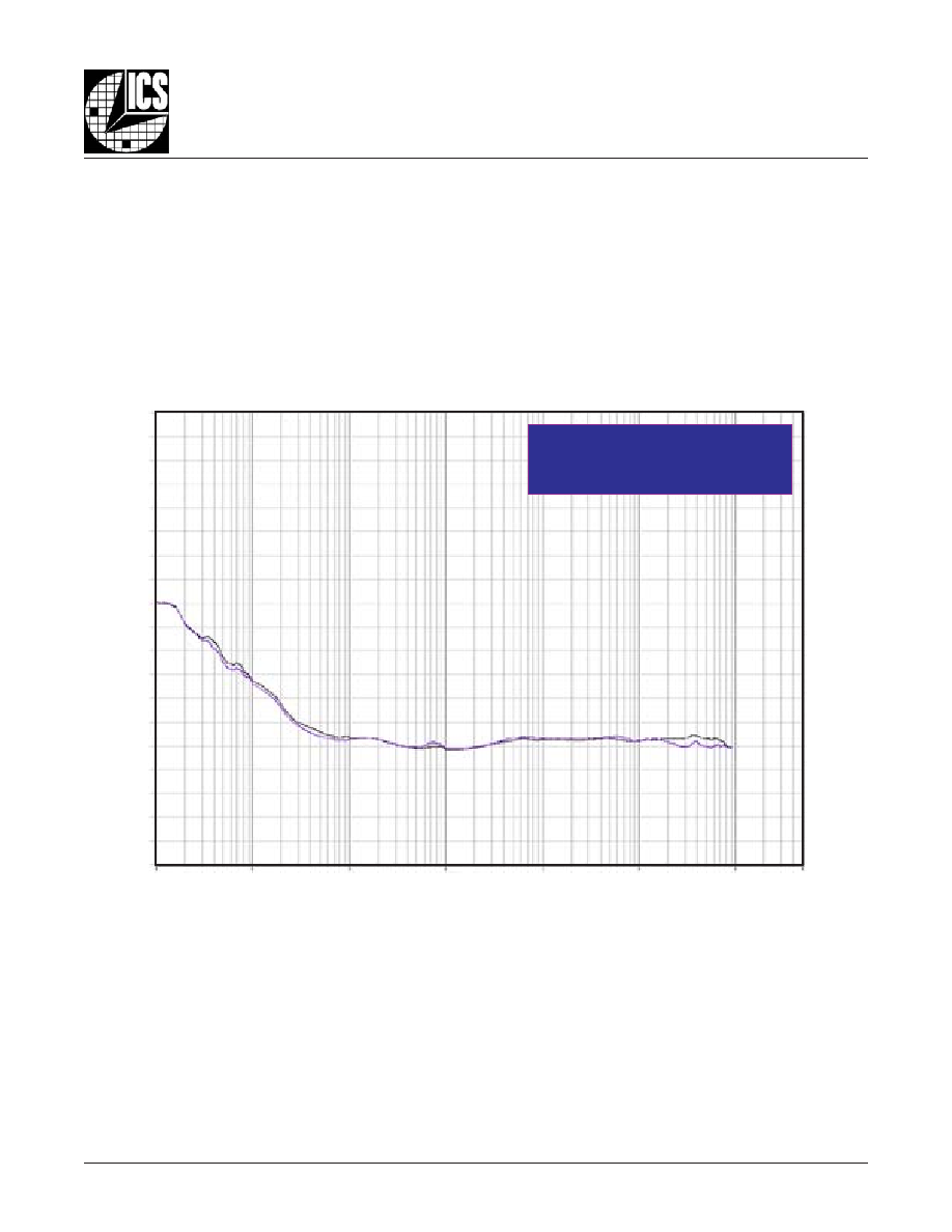
Input/Output Additive Phase Jitter
@ 200MHz (12KHz to 20MHz)
= 0.05ps typical
0
-10
-20
-30
-40
-50
-60
-70
-80
-90
-100
-110
-120
-130
-140
-150
-160
-170
-180
-190
100
1k
10k
100k
1M
10M
100M
500M
The spectral purity in a band at a specific offset from the funda-
mental compared to the power of the fundamental is called the
dBc Phase Noise. This value is normally expressed using a
Phase noise plot and is most often the specified plot in many
applications. Phase noise is defined as the ratio of the noise
power present in a 1Hz band at a specified offset from the fun-
damental frequency to the power value of the fundamental. This
ratio is expressed in decibels (dBm) or a ratio of the power in
As with most timing specifications, phase noise measurements
have issues. The primary issue relates to the limitations of the
equipment. Often the noise floor of the equipment is higher than
the noise floor of the device. This is illustrated above. The de-
the 1Hz band to the power in the fundamental. When the re-
quired offset is specified, the phase noise is called a
dBc value,
which simply means dBm at a specified offset from the funda-
mental. By investigating jitter in the frequency domain, we get a
better understanding of its effects on the desired application over
the entire time record of the signal. It is mathematically possible
to calculate an expected bit error rate given a phase noise plot.
vice meets the noise floor of what is shown, but can actually be
lower. The phase noise is dependant on the input source and
measurement equipment.
O
FFSET
F
ROM
C
ARRIER
F
REQUENCY
(H
Z
)
SSB P
HASE
N
OISE
dBc/H
Z
Document Outline
- General Description
- Features
- Block Diagram
- Pin Assignment
- Pin Descriptions
- Pin Characteristics
- Absolute Maximum Ratings
- Power Supply DC Characteristics
- Differential DC Characteristics
- LVDS DC Characteristics
- AC Characteristics
- Additive Phase Jitter
- Parameter Measurement Information
- 3.3V Output Load AC Test Circuit Diagram
- Differential Input Level Diagram
- Part-to-Part Skew Diagram
- Output Skew Diagram
- Propagation Delay Diagram
- Output Rise/Fall Time Diagram
- Output Duty Cycle/Pulse Width/Period Diagram
- Differential Output Voltage Setup Diagram
- Offset Voltage Setup Diagram
- Power Off Leakage Setup Diagram
- Output Short Circuit Current Setup Diagram
- Differential Output Short Circuit Current Setup Diagram
- Application Information
- Wiring the Differential Input to Accept Single Ended Levels
- Single Ended Signal Driving Differential Input Diagram
- LVDS Driver Termination
- Differential Clock Input Interface
- HiPerClocks CLK/nCLK Input Driven by ICS HiPerClockS LVHSTL Driver Diagram
- HiPerClocks CLK/nCLK Input Driven by 3.3V LVPECL Driver Diagrams
- HiPerClocks CLK/nCLK Input Driven by 3.3V LVDS Driver Diagram
- HiPerClocks CLK/nCLK Input Driven by 3.3V LVPECL Driver w/AC Couple Diagram
- Reliability Information
- Transistor Count
- Package Outline
- Package Dimensions
- Ordering Information
- Revision History Sheet