 | –≠–ª–µ–∫—Ç—Ä–æ–Ω–Ω—ã–π –∫–æ–º–ø–æ–Ω–µ–Ω—Ç: ICS8547AY | –°–∫–∞—á–∞—Ç—å:  PDF PDF  ZIP ZIP |
Document Outline
- General Description
- Features
- Block Diagram
- Pin Assignment
- Pin Descriptions
- Pin Characteristics
- Clock Input Function Table
- Absolute Maximum Ratings
- Power Supply DC Characteristics
- Differential DC Characteristics
- LVDS DC Characteristics
- AC Characteristics
- Parameter Measurement Information
- 3.3V Output Load AC Test Circuit Diagram
- Differential Input Level Diagram
- Part-to-Part Skew Diagram
- Output Skew Diagram
- Bank Skew Diagram
- Output Rise/Fall Time Diagram
- odc & tPeriod Diagram
- Propagation Delay Diagram
- VOD Setup Diagram
- VOS Setup Diagram
- IOS Setup Diagram
- IOSD Setup Diagram
- IOFF Setup Diagram
- Application Information
- Wiring the Differential Input to Accept Single Ended Levels
- Single ended Signal Driving Differential Input Diagram
- Differential Clock Input Interface
- HiPerClockS CLK/nCLK Input Driven by ICS HiPerClockS LVHSTL Driver Diagram
- HiPerClockS CLK/nCLK Input Driven by 3.3V LVPECL Driver Diagrams
- HiPerClockS CLK/nCLK Input Driven by 3.3V LVPECL w/AC Couple Driver Diagrams
- LVDS Driver Termination
- Typical LVDS Driver Termination Diagram
- Reliability Information
- Transistor Count
- Package Outline
- Package Dimensions
- Ordering Information

ICS8547AY
www.icst.com/products/hiperclocks.html
REV. A FEBRUARY 4, 2003
1
Integrated
Circuit
Systems, Inc.
HiPerClockSTM
,&6
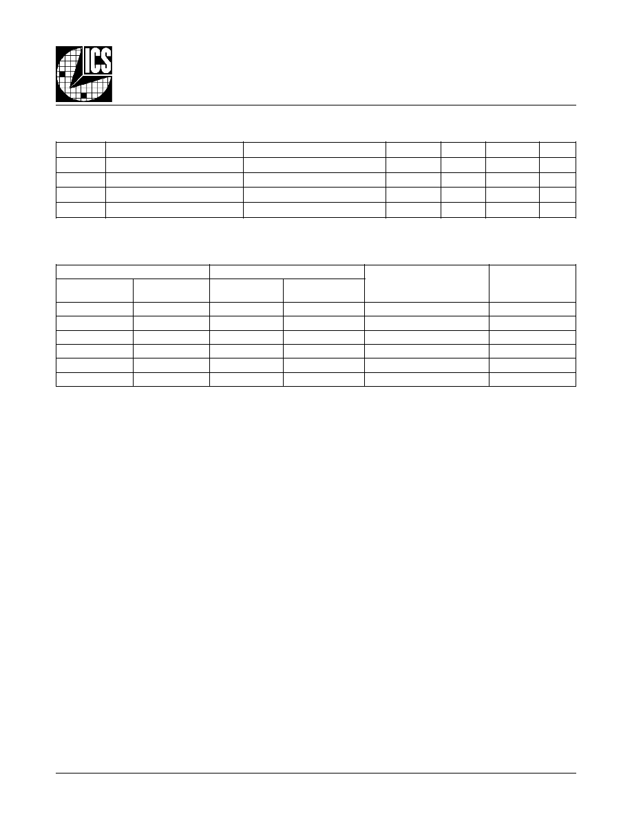
4
8 47 46 45 44 43 42 41 40 39 38 37
13 14 15 16 17 18 19 20 21 22 23 24
1
2
3
4
5
6
7
8
9
10
11
12
36
35
34
33
32
31
30
29
28
27
26
25
Q4A
nQ4A
nQ4B
Q4B
nCLK4
CLK4
CLK5
nCLK5
Q5B
nQ5B
nQ5A
Q5A
Q2A
nQ2A
nQ2B
Q2B
nCLK2
CLK2
CLK1
nCLK1
Q1B
nQ1B
nQ1A
Q1A
V
DDO
GND
V
DD
Q0B
nQ0B
nQ0A
Q0A
nCLK0
CLK0
V
DD
GND
V
DDO
48-Lead LQFP
7mm x 7mm x 1.4mm package body
Y Package
Top View
ICS8547
V
DDO
GND
V
DD
Q3B
nQ3B
nQ3A
Q3A
nCLK3
CLK3
V
DD
GND
V
DDO
CLK0
nCLK0
Q0A
nQ0A
Q0B
nQ0B
CLK1
nCLK1
Q1A
nQ1A
Q1B
nQ1B
CLK2
nCLK2
Q2A
nQ2A
Q2B
nQ2B
CLK3
nCLK3
Q3A
nQ3A
Q3B
nQ3B
CLK4
nCLK4
Q4A
nQ4A
Q4B
nQ4B
CLK5
nCLK5
Q5A
nQ5A
Q5B
nQ5B
ICS8547
H
EX
, L
OW
S
KEW
, 1-
TO
-2
D
IFFERENTIAL
-
TO
-LVDS C
LOCK
B
UFFERS
G
ENERAL
D
ESCRIPTION
The ICS8547 is a Hex low skew, high perfor-
mance 1-to-2 Differential-to-LVDS Clock Buffer
and a member of the HiPerClockSTM family of High
Performance Clock Solutions from ICS. Utilizing
Low Voltage Differential Signaling (LVDS) the
ICS8547 provides a low power, low noise, point-to-point solu-
tion for distributing clock signals over controlled impedances
of 100
. The ICS8547 has six selectable clock inputs. The
CLKx, nCLKx pairs can accept any differential input levels
and translates them to 3.3V LVDS output levels.
Guaranteed output and part-to-part skew specifications make
the ICS8547 ideal for those applications demanding well
defined performance and repeatability.
B
LOCK
D
IAGRAM
P
IN
A
SSIGNMENT
F
EATURES
∑
12 LVDS outputs
∑
Selectable CLKx, nCLKx inputs
∑
CLKx, nCLKx pair can accept the following differential
input levels: LVPECL, LVDS, LVHSTL, HCSL, SSTL
∑
Maximum output frequency: 700MHz
∑
Translates any differential input signal (LVPECL, LVHSTL,
SSTL, DCM) to LVDS levels without external bias networks
∑
Translates any single-ended input signal to LVDS
with resistor bias on nCLKx input
∑
Output skew: 250ps (maximum)
∑
Bank skew: 15ps (maximum)
∑
Part-to-part skew: 500ps (maximum)
∑
Propagation delay: 1.8ns (maximum)
∑
3.3V operating supply
∑
0∞C to 85∞C ambient operating temperature
∑
Industrial temperature information available upon request

ICS8547AY
www.icst.com/products/hiperclocks.html
REV. A FEBRUARY 4, 2003
2
Integrated
Circuit
Systems, Inc.
ICS8547
H
EX
, L
OW
S
KEW
, 1-
TO
-2
D
IFFERENTIAL
-
TO
-LVDS C
LOCK
B
UFFERS
T
ABLE
1. P
IN
D
ESCRIPTIONS
r
e
b
m
u
N
e
m
a
N
e
p
y
T
n
o
i
t
p
i
r
c
s
e
D
2
,
1
A
4
Q
n
,
A
4
Q
t
u
p
t
u
O
.
s
l
e
v
e
l
e
c
a
f
r
e
t
n
i
S
D
V
L
.
r
i
a
p
t
u
p
t
u
o
l
a
i
t
n
e
r
e
f
f
i
D
4
,
3
B
4
Q
,
B
4
Q
n
t
u
p
t
u
O
.
s
l
e
v
e
l
e
c
a
f
r
e
t
n
i
S
D
V
L
.
r
i
a
p
t
u
p
t
u
o
l
a
i
t
n
e
r
e
f
f
i
D
5
4
K
L
C
n
t
u
p
n
I
p
u
ll
u
P
.
t
u
p
n
i
k
c
o
l
c
l
a
i
t
n
e
r
e
f
f
i
d
g
n
i
t
r
e
v
n
I
6
4
K
L
C
t
u
p
n
I
n
w
o
d
ll
u
P
.
t
u
p
n
i
k
c
o
l
c
l
a
i
t
n
e
r
e
f
f
i
d
g
n
i
t
r
e
v
n
i
-
n
o
N
7
5
K
L
C
t
u
p
n
I
n
w
o
d
ll
u
P
.
t
u
p
n
i
k
c
o
l
c
l
a
i
t
n
e
r
e
f
f
i
d
g
n
i
t
r
e
v
n
i
-
n
o
N
8
5
K
L
C
n
t
u
p
n
I
p
u
ll
u
P
.
t
u
p
n
i
k
c
o
l
c
l
a
i
t
n
e
r
e
f
f
i
d
g
n
i
t
r
e
v
n
I
0
1
,
9
B
5
Q
n
,
B
5
Q
t
u
p
t
u
O
.
s
l
e
v
e
l
e
c
a
f
r
e
t
n
i
S
D
V
L
.
r
i
a
p
t
u
p
t
u
o
l
a
i
t
n
e
r
e
f
f
i
D
2
1
,
1
1
A
5
Q
,
A
5
Q
n
t
u
p
t
u
O
.
s
l
e
v
e
l
e
c
a
f
r
e
t
n
i
S
D
V
L
.
r
i
a
p
t
u
p
t
u
o
l
a
i
t
n
e
r
e
f
f
i
D
8
4
,
7
3
,
4
2
,
3
1
V
O
D
D
r
e
w
o
P
.
s
n
i
p
y
l
p
p
u
s
t
u
p
t
u
O
7
4
,
8
3
,
3
2
,
4
1
D
N
G
r
e
w
o
P
.
d
n
u
o
r
g
y
l
p
p
u
s
r
e
w
o
P
6
4
,
9
3
,
2
2
,
5
1
V
D
D
r
e
w
o
P
.
s
n
i
p
y
l
p
p
u
s
e
r
o
C
6
1
0
K
L
C
t
u
p
n
I
n
w
o
d
ll
u
P
.
t
u
p
n
i
k
c
o
l
c
l
a
i
t
n
e
r
e
f
f
i
d
g
n
i
t
r
e
v
n
i
-
n
o
N
7
1
0
K
L
C
n
t
u
p
n
I
p
u
ll
u
P
.
t
u
p
n
i
k
c
o
l
c
l
a
i
t
n
e
r
e
f
f
i
d
g
n
i
t
r
e
v
n
I
9
1
,
8
1
A
0
Q
n
,
A
0
Q
t
u
p
t
u
O
.
s
l
e
v
e
l
e
c
a
f
r
e
t
n
i
S
D
V
L
.
r
i
a
p
t
u
p
t
u
o
l
a
i
t
n
e
r
e
f
f
i
D
1
2
,
0
2
B
0
Q
,
B
0
Q
n
t
u
p
t
u
O
.
s
l
e
v
e
l
e
c
a
f
r
e
t
n
i
S
D
V
L
.
r
i
a
p
t
u
p
t
u
o
l
a
i
t
n
e
r
e
f
f
i
D
6
2
,
5
2
A
1
Q
n
,
A
1
Q
t
u
p
t
u
O
.
s
l
e
v
e
l
e
c
a
f
r
e
t
n
i
S
D
V
L
.
r
i
a
p
t
u
p
t
u
o
l
a
i
t
n
e
r
e
f
f
i
D
8
2
,
7
2
B
1
Q
,
B
1
Q
n
t
u
p
t
u
O
.
s
l
e
v
e
l
e
c
a
f
r
e
t
n
i
S
D
V
L
.
r
i
a
p
t
u
p
t
u
o
l
a
i
t
n
e
r
e
f
f
i
D
9
2
1
K
L
C
n
t
u
p
n
I
p
u
ll
u
P
.
t
u
p
n
i
k
c
o
l
c
l
a
i
t
n
e
r
e
f
f
i
d
g
n
i
t
r
e
v
n
I
0
3
1
K
L
C
t
u
p
n
I
n
w
o
d
ll
u
P
.
t
u
p
n
i
k
c
o
l
c
l
a
i
t
n
e
r
e
f
f
i
d
g
n
i
t
r
e
v
n
i
-
n
o
N
1
3
2
K
L
C
t
u
p
n
I
n
w
o
d
ll
u
P
.
t
u
p
n
i
k
c
o
l
c
l
a
i
t
n
e
r
e
f
f
i
d
g
n
i
t
r
e
v
n
i
-
n
o
N
2
3
2
K
L
C
n
t
u
p
n
I
p
u
ll
u
P
.
t
u
p
n
i
k
c
o
l
c
l
a
i
t
n
e
r
e
f
f
i
d
g
n
i
t
r
e
v
n
I
4
3
,
3
3
B
2
Q
n
,
B
2
Q
t
u
p
t
u
O
.
s
l
e
v
e
l
e
c
a
f
r
e
t
n
i
S
D
V
L
.
r
i
a
p
t
u
p
t
u
o
l
a
i
t
n
e
r
e
f
f
i
D
6
3
,
5
3
A
2
Q
,
A
2
Q
n
t
u
p
t
u
O
.
s
l
e
v
e
l
e
c
a
f
r
e
t
n
i
S
D
V
L
.
r
i
a
p
t
u
p
t
u
o
l
a
i
t
n
e
r
e
f
f
i
D
1
4
,
0
4
B
3
Q
n
,
B
3
Q
t
u
p
t
u
O
.
s
l
e
v
e
l
e
c
a
f
r
e
t
n
i
S
D
V
L
.
r
i
a
p
t
u
p
t
u
o
l
a
i
t
n
e
r
e
f
f
i
D
3
4
,
2
4
A
3
Q
,
A
3
Q
n
t
u
p
t
u
O
.
s
l
e
v
e
l
e
c
a
f
r
e
t
n
i
S
D
V
L
.
r
i
a
p
t
u
p
t
u
o
l
a
i
t
n
e
r
e
f
f
i
D
4
4
3
K
L
C
n
t
u
p
n
I
p
u
ll
u
P
.
t
u
p
n
i
k
c
o
l
c
l
a
i
t
n
e
r
e
f
f
i
d
g
n
i
t
r
e
v
n
I
5
4
3
K
L
C
t
u
p
n
I
n
w
o
d
ll
u
P
.
t
u
p
n
i
k
c
o
l
c
l
a
i
t
n
e
r
e
f
f
i
d
g
n
i
t
r
e
v
n
i
-
n
o
N
:
E
T
O
N
p
u
ll
u
P
d
n
a
n
w
o
d
ll
u
P
.
s
e
u
l
a
v
l
a
c
i
p
y
t
r
o
f
,
s
c
i
t
s
i
r
e
t
c
a
r
a
h
C
n
i
P
,
2
e
l
b
a
T
e
e
S
.
s
r
o
t
s
i
s
e
r
t
u
p
n
i
l
a
n
r
e
t
n
i
o
t
r
e
f
e
r
ICS8547AY
www.icst.com/products/hiperclocks.html
REV. A FEBRUARY 4, 2003
3
Integrated
Circuit
Systems, Inc.
ICS8547
H
EX
, L
OW
S
KEW
, 1-
TO
-2
D
IFFERENTIAL
-
TO
-LVDS C
LOCK
B
UFFERS
T
ABLE
2. P
IN
C
HARACTERISTICS
T
ABLE
3. C
LOCK
I
NPUT
F
UNCTION
T
ABLE
l
o
b
m
y
S
r
e
t
e
m
a
r
a
P
s
n
o
i
t
i
d
n
o
C
t
s
e
T
m
u
m
i
n
i
M
l
a
c
i
p
y
T
m
u
m
i
x
a
M
s
t
i
n
U
C
N
I
e
c
n
a
t
i
c
a
p
a
C
t
u
p
n
I
4
F
p
R
P
U
L
L
U
P
r
o
t
s
i
s
e
R
p
u
ll
u
P
t
u
p
n
I
1
5
K
R
N
W
O
D
L
L
U
P
r
o
t
s
i
s
e
R
n
w
o
d
ll
u
P
t
u
p
n
I
1
5
K
C
D
P
n
o
i
t
a
p
i
s
s
i
D
r
e
w
o
P
e
c
n
a
t
i
c
a
p
a
C
1
F
p
s
t
u
p
n
I
s
t
u
p
t
u
O
e
d
o
M
t
u
p
t
u
O
o
t
t
u
p
n
I
y
t
i
r
a
l
o
P
x
K
L
C
x
K
L
C
n
,
A
5
Q
:
A
0
Q
B
5
Q
:
B
0
Q
,
A
5
Q
n
:
A
0
Q
n
B
5
Q
n
:
B
5
Q
n
0
1
W
O
L
H
G
I
H
l
a
i
t
n
e
r
e
f
f
i
D
o
t
l
a
i
t
n
e
r
e
f
f
i
D
g
n
i
t
r
e
v
n
I
n
o
N
1
0
H
G
I
H
W
O
L
l
a
i
t
n
e
r
e
f
f
i
D
o
t
l
a
i
t
n
e
r
e
f
f
i
D
g
n
i
t
r
e
v
n
I
n
o
N
0
1
E
T
O
N
;
d
e
s
a
i
B
W
O
L
H
G
I
H
l
a
i
t
n
e
r
e
f
f
i
D
o
t
d
e
d
n
E
e
l
g
n
i
S
g
n
i
t
r
e
v
n
I
n
o
N
1
1
E
T
O
N
;
d
e
s
a
i
B
H
G
I
H
W
O
L
l
a
i
t
n
e
r
e
f
f
i
D
o
t
d
e
d
n
E
e
l
g
n
i
S
g
n
i
t
r
e
v
n
I
n
o
N
1
E
T
O
N
;
d
e
s
a
i
B
0
H
G
I
H
W
O
L
l
a
i
t
n
e
r
e
f
f
i
D
o
t
d
e
d
n
E
e
l
g
n
i
S
g
n
i
t
r
e
v
n
I
1
E
T
O
N
;
d
e
s
a
i
B
1
W
O
L
H
G
I
H
l
a
i
t
n
e
r
e
f
f
i
D
o
t
d
e
d
n
E
e
l
g
n
i
S
g
n
i
t
r
e
v
n
I
.
"
s
l
e
v
e
L
d
e
d
n
E
e
l
g
n
i
S
t
p
e
c
c
A
o
t
t
u
p
n
I
l
a
i
t
n
e
r
e
f
f
i
D
e
h
t
g
n
i
r
i
W
"
,
n
o
i
t
c
e
s
n
o
i
t
a
m
r
o
f
n
I
n
o
i
t
a
c
il
p
p
A
e
h
t
o
t
r
e
f
e
r
e
s
a
e
l
P
:
1
E
T
O
N
ICS8547AY
www.icst.com/products/hiperclocks.html
REV. A FEBRUARY 4, 2003
4
Integrated
Circuit
Systems, Inc.
ICS8547
H
EX
, L
OW
S
KEW
, 1-
TO
-2
D
IFFERENTIAL
-
TO
-LVDS C
LOCK
B
UFFERS
T
ABLE
4A. P
OWER
S
UPPLY
DC C
HARACTERISTICS
,
V
DD
= V
DDO
= 3.3V±5%, T
A
= 0∞C
TO
85∞C
T
ABLE
4B. D
IFFERENTIAL
DC C
HARACTERISTICS
,
V
DD
= V
DDO
= 3.3V±5%, T
A
= 0∞C
TO
85∞C
T
ABLE
4C. LVDS DC C
HARACTERISTICS
,
V
DD
= V
DDO
= 3.3V±5%, T
A
= 0∞C
TO
85∞C
l
o
b
m
y
S
r
e
t
e
m
a
r
a
P
s
n
o
i
t
i
d
n
o
C
t
s
e
T
m
u
m
i
n
i
M
l
a
c
i
p
y
T
m
u
m
i
x
a
M
s
t
i
n
U
I
H
I
t
n
e
r
r
u
C
h
g
i
H
t
u
p
n
I
x
K
L
C
V
N
I
V
=
D
D
V
5
6
4
.
3
=
0
5
1
A
µ
x
K
L
C
n
V
N
I
V
=
D
D
V
5
6
4
.
3
=
5
A
µ
I
L
I
t
n
e
r
r
u
C
w
o
L
t
u
p
n
I
x
K
L
C
V
D
D
V
,
V
5
6
4
.
3
=
N
I
V
0
=
5
-
A
µ
x
K
L
C
n
V
D
D
V
,
V
5
6
4
.
3
=
N
I
V
0
=
0
5
1
-
A
µ
V
P
P
e
g
a
t
l
o
V
k
a
e
P
-
o
t
-
k
a
e
P
5
1
.
0
3
.
1
V
V
R
M
C
e
g
n
a
R
e
g
a
t
l
o
V
e
d
o
M
n
o
m
m
o
C
5
.
0
V
D
D
5
8
.
0
-
V
l
o
b
m
y
S
r
e
t
e
m
a
r
a
P
s
n
o
i
t
i
d
n
o
C
t
s
e
T
m
u
m
i
n
i
M
l
a
c
i
p
y
T
m
u
m
i
x
a
M
s
t
i
n
U
V
D
O
e
g
a
t
l
o
V
t
u
p
t
u
O
l
a
i
t
n
e
r
e
f
f
i
D
5
7
1
5
7
2
5
7
3
V
m
V
D
O
V
D
O
e
g
n
a
h
C
e
d
u
t
i
n
g
a
M
0
5
V
m
V
S
O
e
g
a
t
l
o
V
t
e
s
f
f
O
0
.
1
3
.
1
6
.
1
V
V
S
O
V
S
O
e
g
n
a
h
C
e
d
u
t
i
n
g
a
M
0
5
V
m
I
F
F
O
e
g
a
k
a
e
L
f
f
O
r
e
w
o
P
1
-
1
+
A
µ
I
D
S
O
t
n
e
r
r
u
C
t
i
u
c
r
i
C
t
r
o
h
S
t
u
p
t
u
O
l
a
i
t
n
e
r
e
f
f
i
D
5
.
5
-
A
m
I
S
O
I
/
B
S
O
t
n
e
r
r
u
C
t
i
u
c
r
i
C
t
r
o
h
S
t
u
p
t
u
O
2
1
-
A
m
l
o
b
m
y
S
r
e
t
e
m
a
r
a
P
s
n
o
i
t
i
d
n
o
C
t
s
e
T
m
u
m
i
n
i
M
l
a
c
i
p
y
T
m
u
m
i
x
a
M
s
t
i
n
U
V
D
D
e
g
a
t
l
o
V
y
l
p
p
u
S
e
r
o
C
5
3
1
.
3
3
.
3
5
6
4
.
3
V
V
D
D O
e
g
a
t
l
o
V
y
l
p
p
u
S
t
u
p
t
u
O
5
3
1
.
3
3
.
3
5
6
4
.
3
V
I
D
D
t
n
e
r
r
u
C
y
l
p
p
u
S
r
e
w
o
P
2
2
A
m
I
O
D
D
t
n
e
r
r
u
C
y
l
p
p
u
S
t
u
p
t
u
O
8
1
A
m
A
BSOLUTE
M
AXIMUM
R
ATINGS
Supply Voltage, V
DD
4.6V
Inputs, V
I
-0.5V to V
DD
+ 0.5 V
Outputs, V
O
-0.5V to V
DDO
+ 0.5V
Package Thermal Impedance,
JA
47.9∞C/W (0 lfpm)
Storage Temperature, T
STG
-65∞C to 150∞C
NOTE: Stresses beyond those listed under Absolute
Maximum Ratings may cause permanent damage to the
device. These ratings are stress specifications only. Functional
operation of product at these conditions or any conditions be-
yond those listed in the
DC Characteristics or AC Character-
istics is not implied. Exposure to absolute maximum rating
conditions for extended periods may affect product reliability.
ICS8547AY
www.icst.com/products/hiperclocks.html
REV. A FEBRUARY 4, 2003
5
Integrated
Circuit
Systems, Inc.
ICS8547
H
EX
, L
OW
S
KEW
, 1-
TO
-2
D
IFFERENTIAL
-
TO
-LVDS C
LOCK
B
UFFERS
T
ABLE
5. AC C
HARACTERISTICS
,
V
DD
= V
DDO
= 3.3V±5%, T
A
= 0∞C
TO
85∞C
l
o
b
m
y
S
r
e
t
e
m
a
r
a
P
s
n
o
i
t
i
d
n
o
C
t
s
e
T
m
u
m
i
n
i
M
l
a
c
i
p
y
T
m
u
m
i
x
a
M
s
t
i
n
U
f
X
A
M
y
c
n
e
u
q
e
r
F
t
u
p
t
u
O
0
0
7
z
H
M
t
D
P
1
E
T
O
N
;
y
a
l
e
D
n
o
i
t
a
g
a
p
o
r
P
z
H
M
0
0
5
2
.
1
5
.
1
8
.
1
s
n
t
)
o
(
k
s
5
,
2
E
T
O
N
;
w
e
k
S
t
u
p
t
u
O
0
5
2
s
p
t
)
b
(
k
s
5
,
3
E
T
O
N
;
w
e
k
S
k
n
a
B
5
1
s
p
t
)
p
p
(
k
s
5
,
4
E
T
O
N
;
w
e
k
S
t
r
a
P
-
o
t
-
t
r
a
P
0
0
5
s
p
t
R
t
/
F
e
m
i
T
ll
a
F
/
e
s
i
R
t
u
p
t
u
O
%
0
8
o
t
%
0
2
0
5
2
0
5
5
s
p
c
d
o
e
l
c
y
C
y
t
u
D
t
u
p
t
u
O
z
H
M
0
0
3
5
4
0
5
5
5
%
<
z
H
M
0
0
3
z
H
M
0
0
5
0
4
0
6
%
.
e
s
i
w
r
e
h
t
o
d
e
t
o
n
s
s
e
l
n
u
z
H
M
0
0
5
t
a
d
e
r
u
s
a
e
m
s
r
e
t
e
m
a
r
a
p
ll
A
.
t
n
i
o
p
g
n
i
s
s
o
r
c
t
u
p
t
u
o
l
a
i
t
n
e
r
e
f
f
i
d
e
h
t
o
t
t
n
i
o
p
g
n
i
s
s
o
r
c
t
u
p
n
i
l
a
i
t
n
e
r
e
f
f
i
d
e
h
t
m
o
r
f
d
e
r
u
s
a
e
M
:
1
E
T
O
N
.
s
n
o
i
t
i
d
n
o
c
d
a
o
l
l
a
u
q
e
h
t
i
w
d
n
a
s
e
g
a
t
l
o
v
y
l
p
p
u
s
e
m
a
s
e
h
t
t
a
s
t
u
p
t
u
o
n
e
e
w
t
e
b
w
e
k
s
s
a
d
e
n
i
f
e
D
:
2
E
T
O
N
.
s
t
n
i
o
p
s
s
o
r
c
l
a
i
t
n
e
r
e
f
f
i
d
t
u
p
t
u
o
e
h
t
t
a
m
o
r
f
d
e
r
u
s
a
e
M
.
s
n
o
i
t
i
d
n
o
c
d
a
o
l
l
a
u
q
e
h
t
i
w
d
n
a
s
e
g
a
t
l
o
v
e
m
a
s
e
h
t
t
a
s
t
u
p
t
u
o
f
o
k
n
a
b
a
n
i
h
t
i
w
w
e
k
s
s
a
d
e
n
i
f
e
D
:
3
E
T
O
N
d
n
a
s
e
g
a
t
l
o
v
y
l
p
p
u
s
e
m
a
s
e
h
t
t
a
g
n
i
t
a
r
e
p
o
s
e
c
i
v
e
d
t
n
e
r
e
f
f
i
d
n
o
s
t
u
p
t
u
o
n
e
e
w
t
e
b
s
a
d
e
n
i
f
e
D
:
4
E
T
O
N
d
e
r
u
s
a
e
m
e
r
a
s
t
u
p
t
u
o
e
h
t
,
e
c
i
v
e
d
h
c
a
e
n
o
s
t
u
p
n
i
f
o
e
p
y
t
e
m
a
s
e
h
t
g
n
i
s
U
.
s
n
o
i
t
i
d
n
o
c
d
a
o
l
l
a
u
q
e
h
t
i
w
.
s
t
n
i
o
p
s
s
o
r
c
l
a
i
t
n
e
r
e
f
f
i
d
e
h
t
t
a
.
5
6
d
r
a
d
n
a
t
S
C
E
D
E
J
h
t
i
w
e
c
n
a
d
r
o
c
c
a
n
i
d
e
n
i
f
e
d
s
i
r
e
t
e
m
a
r
a
p
s
i
h
T
:
5
E
T
O
N

ICS8547AY
www.icst.com/products/hiperclocks.html
REV. A FEBRUARY 4, 2003
6
Integrated
Circuit
Systems, Inc.
ICS8547
H
EX
, L
OW
S
KEW
, 1-
TO
-2
D
IFFERENTIAL
-
TO
-LVDS C
LOCK
B
UFFERS
P
ARAMETER
M
EASUREMENT
I
NFORMATION
D
IFFERENTIAL
I
NPUT
L
EVEL
3.3V O
UTPUT
L
OAD
AC T
EST
C
IRCUIT
SCOPE
Qx
nQx
LVDS
3.3V±5%
POWER SUPPLY
+
-
Float GND
3.3V
P
ART
-
TO
-P
ART
S
KEW
V
CMR
Cross Points
V
PP
GND
CLKx
nCLKx
V
DD
P
ROPAGATION
D
ELAY
O
UTPUT
R
ISE
/F
ALL
T
IME
Clock Outputs
20%
80%
20%
80%
t
R
t
F
V
O D
tsk(o)
Qx
Qy
O
UTPUT
S
KEW
tsk(pp)
PART 1
PART 2
CLKx
t
PD
odc & t
P
ERIOD
Pulse Width
t
PERIOD
t
PW
t
PERIOD
odc =
QxA, QxB
nCLKx
nQx
nQy
Qx
Qy
nQx
nQy
nQxA, nQxB
QxA, QxB
nQxA, nQxB
B
ANK
S
KEW
tsk(b)
QxA,
nQxA
QxA,
nQxA
QxB,
nQxB
QxB,
nQxB
ICS8547AY
www.icst.com/products/hiperclocks.html
REV. A FEBRUARY 4, 2003
7
Integrated
Circuit
Systems, Inc.
ICS8547
H
EX
, L
OW
S
KEW
, 1-
TO
-2
D
IFFERENTIAL
-
TO
-LVDS C
LOCK
B
UFFERS
V
OS
/
D
VOS
S
ETUP
I
OFF
S
ETUP
I
OSD
S
ETUP
I
OS
S
ETUP
V
OD
/
D
VOD
S
ETUP
out
out
LVDS
DC Input
V
OS
/
V
OS
V
DD
100
out
out
LVDS
DC Input
V
OD
/
V
OD
V
DD
out
out
LVDS
DC Input
I
OSD
V
DD
out
LVDS
DC Input
I
OS
I
OSB
V
DD
out
LVDS
I
OFF
V
DD
ICS8547AY
www.icst.com/products/hiperclocks.html
REV. A FEBRUARY 4, 2003
8
Integrated
Circuit
Systems, Inc.
ICS8547
H
EX
, L
OW
S
KEW
, 1-
TO
-2
D
IFFERENTIAL
-
TO
-LVDS C
LOCK
B
UFFERS
A
PPLICATION
I
NFORMATION
F
IGURE
1. S
INGLE
E
NDED
S
IGNAL
D
RIVING
D
IFFERENTIAL
I
NPUT
R2
1K
V
DD
CLK_IN
+
-
R1
1K
C1
0.1uF
V_REF
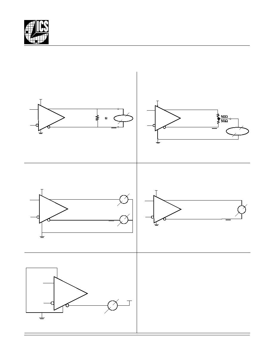
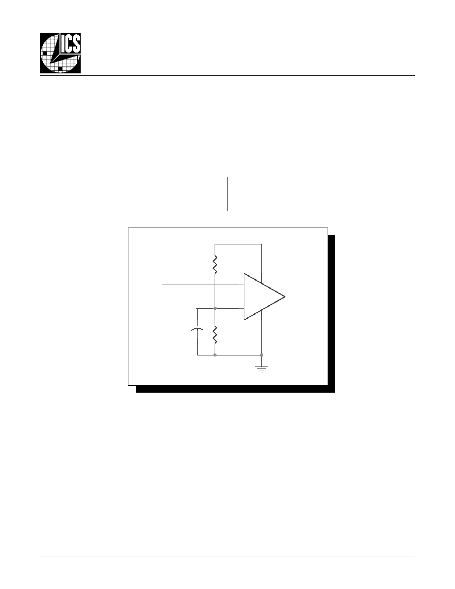
Figure 1 shows how the differential input can be wired to accept
single ended levels. The reference voltage V_REF = V
DD
/2 is
generated by the bias resistors R1, R2 and C1. This bias circuit
should be located as close as possible to the input pin. The ratio
W
IRING
THE
D
IFFERENTIAL
I
NPUT
TO
A
CCEPT
S
INGLE
E
NDED
L
EVELS
of R1 and R2 might need to be adjusted to position the V_REF in
the center of the input voltage swing. For example, if the input
clock swing is only 2.5V and V
DD
= 3.3V, V_REF should be 1.25V
and R2/R1 = 0.609.
ICS8547AY
www.icst.com/products/hiperclocks.html
REV. A FEBRUARY 4, 2003
9
Integrated
Circuit
Systems, Inc.
ICS8547
H
EX
, L
OW
S
KEW
, 1-
TO
-2
D
IFFERENTIAL
-
TO
-LVDS C
LOCK
B
UFFERS
D
IFFERENTIAL
C
LOCK
I
NPUT
I
NTERFACE
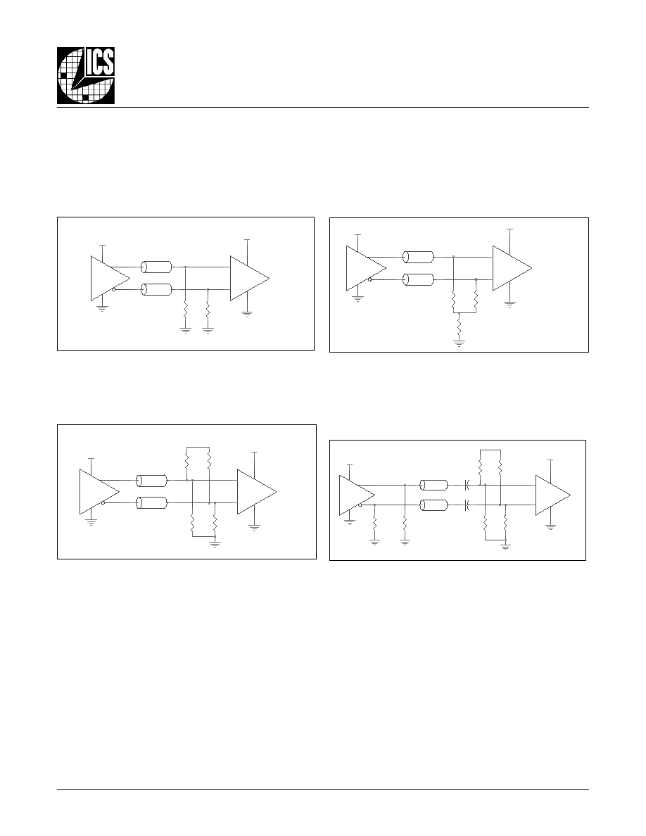
The CLK /nCLK accepts LVDS, LVPECL, LVHSTL, SSTL, HCSL
and other differential signals. Both V
SWING
and V
OH
must meet the
V
PP
and V
CMR
input requirements. Figures 2 to 5 show interface
examples for the HiPerClockS CLK/nCLK input driven by the most
common driver types. The input interfaces suggested here are
examples only. Please consult with the vendor of the driver com-
ponent to confirm the driver termination requirements. For ex-
ample in
Figure 2, the input termination applies for ICS
HiPerClockS LVHSTL drivers. If you are using an LVHSTL driver
from another vendor, use their termination recommendation.
1.8V
R2
50
Input
LVHSTL Driver
ICS
HiPerClockS
R1
50
LVHSTL
3.3V
Zo = 50 Ohm
Zo = 50 Ohm
HiPerClockS
CLK
nCLK
F
IGURE
2. H
I
P
ER
C
LOCK
S CLK/
N
CLK I
NPUT
D
RIVEN
BY
ICS H
I
P
ER
C
LOCK
S LVHSTL D
RIVER
3.3V
R1
50
R3
50
Zo = 50 Ohm
LVPECL
Zo = 50 Ohm
HiPerClockS
CLK
nCLK
3.3V
Input
R2
50
F
IGURE
3. H
I
P
ER
C
LOCK
S CLK/
N
CLK I
NPUT
D
RIVEN
BY
3.3V LVPECL D
RIVER
Zo = 50 Ohm
Input
HiPerClockS
CLK
nCLK
3.3V
R3
125
R2
84
Zo = 50 Ohm
3.3V
R4
125
LVPECL
R1
84
3.3V
Zo = 50 Ohm
R3
125
HiPerClockS
CLK
nCLK
3.3V
R5
100 - 200
3.3V
R2
84
3.3V
R6
100 - 200
Input
R5,R6 locate near the driver pin.
Zo = 50 Ohm
R1
84
R4
125
C2
LVPECL
C1
F
IGURE
4. H
I
P
ER
C
LOCK
S CLK/
N
CLK I
NPUT
D
RIVEN
BY
3.3V LVPECL D
RIVER
F
IGURE
5. H
I
P
ER
C
LOCK
S CLK/
N
CLK I
NPUT
D
RIVEN
BY
3.3V LVPECL D
RIVER
WITH
AC C
OUPLE

ICS8547AY
www.icst.com/products/hiperclocks.html
REV. A FEBRUARY 4, 2003
10
Integrated
Circuit
Systems, Inc.
ICS8547
H
EX
, L
OW
S
KEW
, 1-
TO
-2
D
IFFERENTIAL
-
TO
-LVDS C
LOCK
B
UFFERS
T
RANSISTOR
C
OUNT
The transistor count for ICS8547 is: 1117
T
ABLE
6.
JA
VS
. A
IR
F
LOW
T
ABLE
q
JA
by Velocity (Linear Feet per Minute)
0
200
500
Single-Layer PCB, JEDEC Standard Test Boards
67.8∞C/W
55.9∞C/W
50.1∞C/W
Multi-Layer PCB, JEDEC Standard Test Boards
47.9∞C/W
42.1∞C/W
39.4∞C/W
NOTE: Most modern PCB designs use multi-layered boards. The data in the second row pertains to most designs.
R
ELIABILITY
I
NFORMATION
Zo = 50
R1
100
3.3V
+
-
Zo = 50
LVDS_Driver
3.3V
F
IGURE
6. T
YPICAL
LVDS D
RIVER
T
ERMINATION
LVDS D
RIVER
T
ERMINATION
Figure 6 shows typical termination for LVDS driver in character-
istic impedance of 100
differential (50
single) transmission
line environment. For buffer with multiple LDVS driver, it is rec-
ommended to terminate the unused outputs.
ICS8547AY
www.icst.com/products/hiperclocks.html
REV. A FEBRUARY 4, 2003
11
Integrated
Circuit
Systems, Inc.
ICS8547
H
EX
, L
OW
S
KEW
, 1-
TO
-2
D
IFFERENTIAL
-
TO
-LVDS C
LOCK
B
UFFERS
P
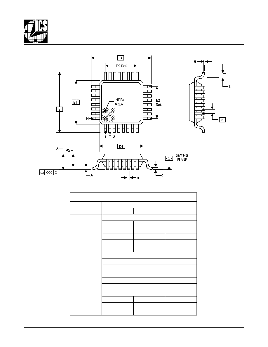
ACKAGE
O
UTLINE
- Y S
UFFIX
T
ABLE
6. P
ACKAGE
D
IMENSIONS
Reference Document: JEDEC Publication 95, MS-026
N
O
I
T
A
I
R
A
V
C
E
D
E
J
S
R
E
T
E
M
I
L
L
I
M
N
I
S
N
O
I
S
N
E
M
I
D
L
L
A
L
O
B
M
Y
S
C
B
B
M
U
M
I
N
I
M
L
A
N
I
M
O
N
M
U
M
I
X
A
M
N
8
4
A
-
-
-
-
0
6
.
1
1
A
5
0
.
0
-
-
5
1
.
0
2
A
5
3
.
1
0
4
.
1
5
4
.
1
b
7
1
.
0
2
2
.
0
7
2
.
0
c
9
0
.
0
-
-
0
2
.
0
D
C
I
S
A
B
0
0
.
9
1
D
C
I
S
A
B
0
0
.
7
2
D
.
f
e
R
0
5
.
5
E
C
I
S
A
B
0
0
.
9
1
E
C
I
S
A
B
0
0
.
7
2
E
.
f
e
R
0
5
.
5
e
C
I
S
A
B
0
5
.
0
L
5
4
.
0
0
6
.
0
5
7
.
0
q
0
∞
-
-
7
∞
c
c
c
-
-
-
-
8
0
.
0
ICS8547AY
www.icst.com/products/hiperclocks.html
REV. A FEBRUARY 4, 2003
12
Integrated
Circuit
Systems, Inc.
ICS8547
H
EX
, L
OW
S
KEW
, 1-
TO
-2
D
IFFERENTIAL
-
TO
-LVDS C
LOCK
B
UFFERS
T
ABLE
7. O
RDERING
I
NFORMATION
While the information presented herein has been checked for both accuracy and reliability, Integrated Circuit Systems, Incorporated (ICS) assumes no responsibility for either its use
or for infringement of any patents or other rights of third parties, which would result from its use. No other circuits, patents, or licenses are implied. This product is intended for use
in normal commercial applications. Any other applications such as those requiring extended temperature range, high reliability, or other extraordinary environmental requirements are
not recommended without additional processing by ICS. ICS reserves the right to change any circuitry or specifications without notice. ICS does not authorize or warrant any ICS
product for use in life support devices or critical medical instruments.
r
e
b
m
u
N
r
e
d
r
O
/
t
r
a
P
g
n
i
k
r
a
M
e
g
a
k
c
a
P
t
n
u
o
C
e
r
u
t
a
r
e
p
m
e
T
Y
A
7
4
5
8
S
C
I
Y
A
7
4
5
8
S
C
I
P
F
Q
L
d
a
e
L
8
4
y
a
r
t
r
e
p
0
5
2
C
∞
5
8
o
t
C
∞
0
T
Y
A
7
4
5
8
S
C
I
Y
A
7
4
5
8
S
C
I
l
e
e
R
d
n
a
e
p
a
T
n
o
P
F
Q
L
d
a
e
L
8
4
0
0
0
1
C
∞
5
8
o
t
C
∞
0