 | –≠–ª–µ–∫—Ç—Ä–æ–Ω–Ω—ã–π –∫–æ–º–ø–æ–Ω–µ–Ω—Ç: ICS858020 | –°–∫–∞—á–∞—Ç—å:  PDF PDF  ZIP ZIP |
Document Outline
- General Description
- Features
- Block Diagram
- Pin Assignment
- Pin Descriptions
- Absolute Maximum Ratings
- Power Supply DC Characteristics
- DC Characteristics
- CML DC Characteristics
- AC Characteristics
- Parameter Measurement Information
- Output Load AC Test Circuit Diagram
- Differential Input Level Diagram
- Part-to-Part Skew Diagram
- Output Skew Diagram
- Propagation Delay Diagram
- Single Ended & Differential Input voltage Swing Diagram
- Output Rise/Fall Time Diagram
- Application Information
- 2.5V LVPECL Input w/Built-In 50ohms Termination Interface
- 3.3V LVPECL Input w/Built-In 50ohms Termination Interface
- 2.5V Differential Input w/Built-In 50ohms Termination Unused Input Handling
- 3.3V Differential Input w/Built-In 50ohms Termination Unused Input Handling
- Schematic Example
- Reliability Information
- Transistor Count
- Package Outline
- Package Dimensions
- Untitled

858020AK
www.icst.com/products/hiperclocks.html
REV. A JULY 9, 2004
1
Integrated
Circuit
Systems, Inc.
ICS858020
L
OW
S
KEW
, 1-
TO
-4
D
IFFERENTIAL
-
TO
-CML F
ANOUT
B
UFFER
PRELIMINARY
G
ENERAL
D
ESCRIPTION
The ICS858020 is a high speed 1-to-4 Differential-
to-CML Fanout Buffer and is a member of the
HiPerClockS
TM
family of high performance clock
solutions from ICS. The ICS858020 is optimized
for high speed and very low output skew, making
it suitable for use in demanding applications such as SONET,
1 Gigabit and 10 Gigabit Ethernet, and Fibre Channel. The
internally terminated differential input and V
REF
_
AC
pin allow
other differential signal families such as LVDS, LVHSTL and
CML to be easily interfaced to the input with minimal use of
external components. The ICS858020 is packaged in a small
3mm x 3mm 16-pin VFQFN package which makes it ideal for
use in space-constrained applications.
F
EATURES
∑ 4 differential CML outputs
∑ 1 LVPECL differential clock input
∑ IN, nIN pair can accept the following differential input levels:
LVPECL, LVDS, CML, SSTL
∑ Output frequency: >2.5GHz (typical)
∑ Output skew: TBD
∑ Part-to-part skew: TBD
∑ Additive phase jitter, RMS: <100fs (typical)
∑ Propagation delay: 465ps (typical)
∑ Operating voltage supply range:
V
CC
= 2.375V to 3.63V, V
EE
= 0V
∑ -40∞C to 85∞C ambient operating temperature
∑ Pin compatible with SY58020U
B
LOCK
D
IAGRAM
P
IN
A
SSIGNMENT
HiPerClockSTM
ICS
IN
V
T
nIN
Q0
nQ0
Q1
nQ1
Q2
nQ2
Q3
nQ3
V
REF_AC
ICS858020
16-Lead VFQFN
3mm x 3mm x 0.95 package body
K Package
Top View
IN
V
T
V
REF
_
AC
nIN
Q1
nQ1
Q2
nQ2
V
EE
nQ3
Q3
V
CC
V
EE
Q0
nQ
0
V
CC
1
2
3
4
12
11
10
9
5 6 7 8
16 15 14 13
The Preliminary Information presented herein represents a product in prototyping or pre-production. The noted characteristics are based on initial
product characterization. Integrated Circuit Systems, Incorporated (ICS) reserves the right to change any circuitry or specifications without notice.
858020AK
www.icst.com/products/hiperclocks.html
REV. A JULY 9, 2004
2
Integrated
Circuit
Systems, Inc.
ICS858020
L
OW
S
KEW
, 1-
TO
-4
D
IFFERENTIAL
-
TO
-CML F
ANOUT
B
UFFER
PRELIMINARY
T
ABLE
1. P
IN
D
ESCRIPTIONS
r
e
b
m
u
N
e
m
a
N
e
p
y
T
n
o
i
t
p
i
r
c
s
e
D
1
N
I
t
u
p
n
I
.
t
u
p
n
i
k
c
o
l
c
l
a
i
t
n
e
r
e
f
f
i
d
L
C
E
P
V
L
g
n
i
t
r
e
v
n
i
-
n
o
N
2
V
T
t
u
p
n
I
.
t
u
p
n
i
n
o
i
t
a
n
i
m
r
e
T
3
V
C
A
_
F
E
R
t
u
p
t
u
O
.
s
n
o
i
t
a
c
il
p
p
a
d
e
l
p
u
o
c
-
C
A
r
o
f
e
g
a
t
l
o
v
e
c
n
e
r
e
f
e
R
V
C
A
_
F
E
R
V
o
t
=
C
C
.
V
8
3
.
1
-
4
N
I
n
t
u
p
n
I
.
t
u
p
n
i
k
c
o
l
c
L
C
E
P
V
L
l
a
i
t
n
e
r
e
f
f
i
d
g
n
i
t
r
e
v
n
I
6
1
,
5
V
E
E
r
e
w
o
P
.
n
i
p
y
l
p
p
u
s
e
v
i
t
a
g
e
N
7
,
6
3
Q
,
3
Q
n
t
u
p
t
u
O
.
s
l
e
v
e
l
e
c
a
f
r
e
t
n
i
L
M
C
.
r
i
a
p
t
u
p
t
u
o
l
a
i
t
n
e
r
e
f
f
i
D
3
1
,
8
V
C
C
r
e
w
o
P
.
s
n
i
p
y
l
p
p
u
s
e
v
i
t
i
s
o
P
0
1
,
9
2
Q
,
2
Q
n
t
u
p
t
u
O
.
s
l
e
v
e
l
e
c
a
f
r
e
t
n
i
L
M
C
.
r
i
a
p
t
u
p
t
u
o
l
a
i
t
n
e
r
e
f
f
i
D
2
1
,
1
1
1
Q
,
1
Q
n
t
u
p
t
u
O
.
s
l
e
v
e
l
e
c
a
f
r
e
t
n
i
L
M
C
.
r
i
a
p
t
u
p
t
u
o
l
a
i
t
n
e
r
e
f
f
i
D
5
1
,
4
1
0
Q
,
0
Q
n
t
u
p
t
u
O
.
s
l
e
v
e
l
e
c
a
f
r
e
t
n
i
L
M
C
.
r
i
a
p
t
u
p
t
u
o
l
a
i
t
n
e
r
e
f
f
i
D

858020AK
www.icst.com/products/hiperclocks.html
REV. A JULY 9, 2004
3
Integrated
Circuit
Systems, Inc.
ICS858020
L
OW
S
KEW
, 1-
TO
-4
D
IFFERENTIAL
-
TO
-CML F
ANOUT
B
UFFER
PRELIMINARY
T
ABLE
2A. P
OWER
S
UPPLY
DC C
HARACTERISTICS
,
V
CC
= 2.375V
TO
3.63V; V
EE
= 0V
l
o
b
m
y
S
r
e
t
e
m
a
r
a
P
s
n
o
i
t
i
d
n
o
C
t
s
e
T
m
u
m
i
n
i
M
l
a
c
i
p
y
T
m
u
m
i
x
a
M
s
t
i
n
U
V
C
C
e
g
a
t
l
o
V
y
l
p
p
u
S
e
v
i
t
i
s
o
P
5
7
3
.
2
3
.
3
3
6
.
3
V
I
E
E
t
n
e
r
r
u
C
y
l
p
p
u
S
r
e
w
o
P
D
B
T
A
m
A
BSOLUTE
M
AXIMUM
R
ATINGS
NOTE: Stresses beyond those listed under Absolute
Maximum Ratings may cause permanent damage
to the device. These ratings are stress specifi-
cations only. Functional operation of product at
these conditions or any conditions beyond those
listed in the
DC Characteristics or AC Character-
istics is not implied. Exposure to absolute maxi-
mum rating conditions for extended periods may
affect product reliability.
Supply Voltage, V
CC
4.6V (CML mode, V
EE
= 0)
Inputs, V
I
-0.5V to V
CC
+ 0.5 V
Outputs, I
O
Continuous Current
20mA
Surge Current
40mA
Input Current, IN, nIN
±50mA
V
T
Current, I
VT
±100mA
Input Sink/Source, I
REF_AC
± 0.5mA
Operating Temperature Range, TA -40∞C to +85∞C
Storage Temperature, T
STG
-65∞C to 150∞C
Package Thermal Impedance,
JA
51.5∞C/W (0 lfpm)
(Junction-to-Ambient)
T
ABLE
2B. DC C
HARACTERISTICS
,
V
CC
= 2.375V
TO
3.63V; V
EE
= 0V
l
o
b
m
y
S
r
e
t
e
m
a
r
a
P
s
n
o
i
t
i
d
n
o
C
t
s
e
T
m
u
m
i
n
i
M
l
a
c
i
p
y
T
m
u
m
i
x
a
M
s
t
i
n
U
R
N
I
e
c
n
a
t
s
i
s
e
R
t
u
p
n
I
l
a
i
t
n
e
r
e
f
f
i
D
)
N
I
n
,
N
I
(
0
0
1
V
H
I
e
g
a
t
l
o
V
h
g
i
H
t
u
p
n
I
)
N
I
n
,
N
I
(
2
.
1
V
C
C
V
V
L
I
e
g
a
t
l
o
V
w
o
L
t
u
p
n
I
)
N
I
n
,
N
I
(
0
V
H
I
5
1
.
0
-
V
V
N
I
1
E
T
O
N
;
g
n
i
w
S
e
g
a
t
l
o
V
t
u
p
n
I
5
1
.
0
8
.
2
V
V
N
I
_
F
F
I
D
g
n
i
w
S
e
g
a
t
l
o
V
t
u
p
n
I
l
a
i
t
n
e
r
e
f
f
i
D
3
.
0
V
I
N
I
t
n
e
r
r
u
C
t
u
p
n
I
)
N
I
n
,
N
I
(
5
3
A
m
.
m
a
r
g
a
i
d
g
n
i
w
S
e
g
a
t
l
o
V
t
u
p
n
I
,
n
o
i
t
a
m
r
o
f
n
I
t
n
e
m
e
r
u
s
a
e
M
r
e
t
e
m
a
r
a
P
o
t
r
e
f
e
R
:
1
E
T
O
N
T
ABLE
2C. CML DC C
HARACTERISTICS
,
V
CC
= 2.375V
TO
3.63V; V
EE
= 0V
l
o
b
m
y
S
r
e
t
e
m
a
r
a
P
s
n
o
i
t
i
d
n
o
C
m
u
m
i
n
i
M
l
a
c
i
p
y
T
m
u
m
i
x
a
M
s
t
i
n
U
V
H
O
1
E
T
O
N
;
e
g
a
t
l
o
V
h
g
i
H
t
u
p
t
u
O
V
C
C
0
2
0
.
0
-
V
C
C
0
1
0
.
0
-
V
C
C
V
V
T
U
O
g
n
i
w
S
e
g
a
t
l
o
V
t
u
p
t
u
O
5
2
3
0
0
4
V
m
V
T
U
O
_
F
F
I
D
g
n
i
w
S
e
g
a
t
l
o
V
t
u
p
t
u
O
l
a
i
t
n
e
r
e
f
f
i
D
0
5
6
0
0
8
V
m
R
T
U
O
e
c
n
a
d
e
p
m
I
e
c
r
u
o
S
t
u
p
t
u
O
0
4
0
5
0
6
0
0
1
h
t
i
w
d
e
t
a
n
i
m
r
e
t
s
t
u
p
t
u
O
:
1
E
T
O
N
.
r
i
a
p
t
u
p
t
u
o
l
a
i
t
n
e
r
e
f
f
i
d
s
s
o
r
c
a

858020AK
www.icst.com/products/hiperclocks.html
REV. A JULY 9, 2004
4
Integrated
Circuit
Systems, Inc.
ICS858020
L
OW
S
KEW
, 1-
TO
-4
D
IFFERENTIAL
-
TO
-CML F
ANOUT
B
UFFER
PRELIMINARY
T
ABLE
3. AC C
HARACTERISTICS
,
V
CC
= 0V; V
EE
= -3.63V
TO
-2.375V
OR
V
CC
= 2.375
TO
3.63V; V
EE
= 0V
l
o
b
m
y
S
r
e
t
e
m
a
r
a
P
n
o
i
t
i
d
n
o
C
m
u
m
i
n
i
M
l
a
c
i
p
y
T
m
u
m
i
x
a
M
s
t
i
n
U
f
X
A
M
y
c
n
e
u
q
e
r
F
t
u
p
t
u
O
5
.
2
>
z
H
G
t
D
P
;
)
l
a
i
t
n
e
r
e
f
f
i
D
(
;
y
a
l
e
D
n
o
i
t
a
g
a
p
o
r
P
1
E
T
O
N
5
6
4
s
p
t
)
o
(
k
s
4
,
2
E
T
O
N
;
w
e
k
S
t
u
p
t
u
O
D
B
T
s
p
t
)
p
p
(
k
s
4
,
3
E
T
O
N
;
w
e
k
S
t
r
a
P
-
o
t
-
t
r
a
P
D
B
T
s
p
t t
ij
;
S
M
R
,
r
e
t
t
i
J
e
s
a
h
P
e
v
i
t
i
d
d
A
r
e
f
f
u
B
n
o
i
t
c
e
s
r
e
t
t
i
J
e
s
a
h
P
e
v
i
t
i
d
d
A
o
t
r
e
f
e
r
0
0
1
<
s
f
t
R
/t
F
e
m
i
T
ll
a
F
/
e
s
i
R
t
u
p
t
u
O
%
0
8
o
t
%
0
2
0
2
1
s
p
t
a
d
e
z
i
r
e
t
c
a
r
a
h
c
s
r
e
t
e
m
a
r
a
p
ll
A
.
d
e
t
o
n
e
s
i
w
r
e
h
t
o
s
s
e
l
n
u
z
H
G
1
R
L
0
0
1
=
.
r
i
a
p
t
u
p
t
u
o
h
c
a
e
r
e
t
f
a
.
t
n
i
o
p
g
n
i
s
s
o
r
c
t
u
p
t
u
o
l
a
i
t
n
e
r
e
f
f
i
d
e
h
t
o
t
t
n
i
o
p
g
n
i
s
s
o
r
c
t
u
p
n
i
l
a
i
t
n
e
r
e
f
f
i
d
e
h
t
m
o
r
f
d
e
r
u
s
a
e
M
:
1
E
T
O
N
.
s
n
o
i
t
i
d
n
o
c
d
a
o
l
l
a
u
q
e
h
t
i
w
d
n
a
e
g
a
t
l
o
v
y
l
p
p
u
s
e
m
a
s
e
h
t
t
a
s
t
u
p
t
u
o
n
e
e
w
t
e
b
w
e
k
s
s
a
d
e
n
i
f
e
D
:
2
E
T
O
N
.
s
t
n
i
o
p
s
s
o
r
c
l
a
i
t
n
e
r
e
f
f
i
d
t
u
p
t
u
o
e
h
t
t
a
d
e
r
u
s
a
e
M
s
e
g
a
t
l
o
v
y
l
p
p
u
s
e
m
a
s
e
h
t
t
a
g
n
i
t
a
r
e
p
o
s
e
c
i
v
e
d
t
n
e
r
e
f
f
i
d
n
o
s
t
u
p
t
u
o
n
e
e
w
t
e
b
w
e
k
s
s
a
d
e
n
i
f
e
D
:
3
E
T
O
N
d
e
r
u
s
a
e
m
e
r
a
s
t
u
p
t
u
o
e
h
t
,
e
c
i
v
e
d
h
c
a
e
n
o
s
t
u
p
n
i
f
o
e
p
y
t
e
m
a
s
e
h
t
g
n
i
s
U
.
s
n
o
i
t
i
d
n
o
c
d
a
o
l
l
a
u
q
e
h
t
i
w
d
n
a
.
s
t
n
i
o
p
s
s
o
r
c
l
a
i
t
n
e
r
e
f
f
i
d
e
h
t
t
a
.
5
6
d
r
a
d
n
a
t
S
C
E
D
E
J
h
t
i
w
e
c
n
a
d
r
o
c
c
a
n
i
d
e
n
i
f
e
d
s
i
r
e
t
e
m
a
r
a
p
s
i
h
T
:
4
E
T
O
N

858020AK
www.icst.com/products/hiperclocks.html
REV. A JULY 9, 2004
5
Integrated
Circuit
Systems, Inc.
ICS858020
L
OW
S
KEW
, 1-
TO
-4
D
IFFERENTIAL
-
TO
-CML F
ANOUT
B
UFFER
PRELIMINARY
P
ARAMETER
M
EASUREMENT
I
NFORMATION
O
UTPUT
L
OAD
AC T
EST
C
IRCUIT
D
IFFERENTIAL
I
NPUT
L
EVEL
O
UTPUT
S
KEW
P
ART
-
TO
-P
ART
S
KEW
O
UTPUT
R
ISE
/F
ALL
T
IME
P
ROPAGATION
D
ELAY
S
INGLE
E
NDED
& D
IFFERENTIAL
I
NPUT
V
OLTAGE
S
WING
V
EE
nIN
V
CC
IN
tsk(pp)
tsk(o)
nQx
Qx
nQy
Qy
PART 1
PART 2
nQx
Qx
nQy
Qy
Clock
Outputs
20%
80%
80%
20%
t
R
t
F
V
SW I N G
t
PD
nIN
Q0:Q3
nQ0:nQ3
IN
V
IH
Cross Points
V
IN
V
IL
SCOPE
nQx
Qx
Power
Supply
V
EE
V
CC
Float
GND
GND
3.3V ± 5%
or
2.5V ± 5%
CML with Internal Pullup
+
-
V
IN
, V
OUT
400mV
(typical)
V
DIFF_IN
, V
DIFF_OUT
800mV
(typical)
V
IN
V
DIF_IN

858020AK
www.icst.com/products/hiperclocks.html
REV. A JULY 9, 2004
6
Integrated
Circuit
Systems, Inc.
ICS858020
L
OW
S
KEW
, 1-
TO
-4
D
IFFERENTIAL
-
TO
-CML F
ANOUT
B
UFFER
PRELIMINARY
LVPECL I
NPUT
WITH
B
UILT
-I
N
50
T
ERMINATION
I
NTERFACE
(2.5V)
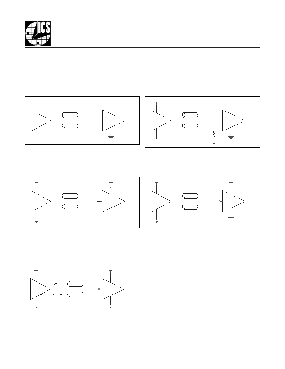
The IN/nIN with built-in 50
terminations accepts LVDS,
LVPECL, LVHSTL, CML, SSTL and other differential signals.
Both V
SWING
and V
OH
must meet the V
PP
and V
CMR
input require-
ments.
Figures 1A to 1D show interface examples for the
HiPerClockS IN/nIN input with built-in 50
terminations driven
by the most common driver types. The input interfaces sug-
gested here are examples only. If the driver is from another
vendor, use their termination recommendation. Please consult
with the vendor of the driver component to confirm the driver
termination requirements.
A
PPLICATION
I
NFORMATION
F
IGURE
1A. H
I
P
ER
C
LOCK
S IN/nIN I
NPUT
WITH
B
UILT
-
IN
50
D
RIVEN
BY
AN
LVDS D
RIVER
F
IGURE
1B. H
I
P
ER
C
LOCK
S IN/nIN I
NPUT
WITH
B
UILT
-
IN
50
D
RIVEN
BY
AN
LVPECL D
RIVER
IN
nIN
VT
2.5V
LVDS
3.3V or 2.5V
Zo = 50 Ohm
Zo = 50 Ohm
Receiver
With
Built-In
50 Ohm
Zo = 50 Ohm
Receiver
With
Built-In
50 Ohm
Zo = 50 Ohm
IN
nIN
VT
2.5V
2.5V
R1
18
2.5V LVPECL
F
IGURE
1E. H
I
P
ER
C
LOCK
S IN/nIN I
NPUT
WITH
B
UILT
-
IN
50
D
RIVEN
BY
AN
SSTL D
RIVER
F
IGURE
1C. H
I
P
ER
C
LOCK
S IN/nIN I
NPUT
WITH
B
UILT
-
IN
50
D
RIVEN
BY
AN
O
PEN
C
OLLECTOR
CML D
RIVER
F
IGURE
1D. H
I
P
ER
C
LOCK
S IN/nIN I
NPUT
WITH
B
UILT
-
IN
50
D
RIVEN
BY
A
CML D
RIVER
WITH
B
UILT
-I
N
50
P
ULLUP
Zo = 50 Ohm
2.5V
Zo = 50 Ohm
IN
nIN
VT
Receiver
With
Built-In
50 Ohm
2.5V
CML - Open Collector
IN
nIN
VT
Receiver
With
Built-In
50 Ohm
2.5V
Zo = 50 Ohm
Zo = 50 Ohm
CML - Built-in 50 Ohm Pull-up
2.5V
2.5V
2.5V
SSTL
R1
25
R2
25
IN
VT
nIN
Receiver With Built-In 50
Zo = 50 Ohm
Zo = 50 Ohm
858020AK
www.icst.com/products/hiperclocks.html
REV. A JULY 9, 2004
7
Integrated
Circuit
Systems, Inc.
ICS858020
L
OW
S
KEW
, 1-
TO
-4
D
IFFERENTIAL
-
TO
-CML F
ANOUT
B
UFFER
PRELIMINARY
LVPECL I
NPUT
WITH
B
UILT
-I
N
50
T
ERMINATION
I
NTERFACE
(3.3V)
The IN /nIN with built-in 50
terminations accepts LVDS,
LVPECL, LVHSTL, CML, SSTL and other differential signals.
Both V
SWING
and V
OH
must meet the V
PP
and V
CMR
input require-
ments.
Figures 2A to 2D show interface examples for the
HiPerClockS IN/nIN input with built-in 50
terminations driven
by the most common driver types. The input interfaces sug-
gested here are examples only. If the driver is from another
vendor, use their termination recommendation. Please consult
with the vendor of the driver component to confirm the driver
termination requirements.
F
IGURE
2A. H
I
P
ER
C
LOCK
S IN/nIN I
NPUT
WITH
B
UILT
-
IN
50
D
RIVEN
BY
AN
LVDS D
RIVER
F
IGURE
2B. H
I
P
ER
C
LOCK
S IN/nIN I
NPUT
WITH
B
UILT
-
IN
50
D
RIVEN
BY
AN
LVPECL D
RIVER
F
IGURE
2D. H
I
P
ER
C
LOCK
S IN/nIN I
NPUT
WITH
B
UILT
-
IN
50
D
RIVEN
BY
A
CML D
RIVER
WITH
B
UILT
-I
N
50
P
ULLUP
3.3V
Zo = 50 Ohm
3.3V
LVDS
Receiver
With
Built-In
50 Ohm
IN
nIN
VT
Zo = 50 Ohm
R1
50
IN
nIN
VT
3.3V
Zo = 50 Ohm
Receiver
With
Built-In
50 Ohm
3.3V
LVPECL
Zo = 50 Ohm
F
IGURE
2E. H
I
P
ER
C
LOCK
S IN/nIN I
NPUT
WITH
B
UILT
-
IN
50
D
RIVEN
BY
AN
SSTL D
RIVER
3.3V
Receiver
With
Built-In
50 Ohm
Zo = 50 Ohm
IN
nIN
VT
3.3V
Zo = 50 Ohm
CML- Built-in 50 Ohm Pull-Up
F
IGURE
2C. H
I
P
ER
C
LOCK
S IN/nIN I
NPUT
WITH
B
UILT
-
IN
50
D
RIVEN
BY
A
CML D
RIVER
WITH
O
PEN
C
OLLECTOR
Zo = 50 Ohm
Zo = 50 Ohm
3.3V
R2
25
Receiver
With
Built-In
50 Ohm
IN
nIN
VT
SSTL
R1
25
3.3V
3.3V
CML- Open Collector
IN
nIN
VT
Zo = 50 Ohm
Receiver
With
Built-In
50 Ohm
3.3V
Zo = 50 Ohm

858020AK
www.icst.com/products/hiperclocks.html
REV. A JULY 9, 2004
8
Integrated
Circuit
Systems, Inc.
ICS858020
L
OW
S
KEW
, 1-
TO
-4
D
IFFERENTIAL
-
TO
-CML F
ANOUT
B
UFFER
PRELIMINARY
Receiver
with
Built-In
50 Ohm
IN
nIN
VT
3.3V
3.3V
R1
1K
R2
1K
F
IGURE
4. U
NUSED
I
NPUT
H
ANDLING
3.3V D
IFFERENTIAL
I
NPUT
WITH
B
UILT
-I
N
50
T
ERMINATION
U
NUSED
I
NPUT
H
ANDLING
To prevent oscillation and to reduce noise, it is recommended to
have pullup and pulldown connect to true and compliment of the
unused input as shown in
Figure 4.
F
IGURE
3. U
NUSED
I
NPUT
H
ANDLING
2.5V D
IFFERENTIAL
I
NPUT
WITH
B
UILT
-I
N
50
T
ERMINATION
U
NUSED
I
NPUT
H
ANDLING
To prevent oscillation and to reduce noise, it is recommended to
have pullup and pulldown connect to true and compliment of the
unused input as shown in
Figure 3.
IN
nIN
VT
2.5V
R2
680
Receiver
with
Built-In
50 Ohm
2.5V
R1
680

858020AK
www.icst.com/products/hiperclocks.html
REV. A JULY 9, 2004
9
Integrated
Circuit
Systems, Inc.
ICS858020
L
OW
S
KEW
, 1-
TO
-4
D
IFFERENTIAL
-
TO
-CML F
ANOUT
B
UFFER
PRELIMINARY
S
CHEMATIC
E
XAMPLE
Figure 5 shows a schematic example of the ICS858020. This
schematic provides examples of input and output handling. The
ICS858020 input has built-in 50
termination resistors. The in-
put can directly accept various types of differential signal with-
out AC couple. If AC couple termination is used, the ICS858020
also provides VREF_AC pin for proper offset level after the AC
Zo = 50
Zo = 50
3.3V
Zo = 50
U1
ICS858020
1
2
3
4
5
6
7
8
9
10
11
12
13
14
15
16
IN
VT
VREF_AC
nIN
VE
E
nQ
3
Q3
VC
C
nQ2
Q2
nQ1
Q1
VC
C
nQ
0
Q0
VE
E
Zo = 50
100 Ohm Dif f erential
+
-
LVPECL
R2
100
R4
100
3.3V
C1
0.1u
Zo = 50
3.3V
C2
0.1u
2.5V
R1
100
C6
C5
Zo = 50
R3
100
3.3V
100 Ohm Dif f erential
+
-
F
IGURE
5. ICS858020 A
PPLICATION
S
CHEMATIC
E
XAMPLE
couple. This example shows the ICS858020 input driven by a
2.5V LVPECL driver with AC couple. The ICS858020 outputs
are CML driver with built-in 50
pull up resistors. In this ex-
ample, we assume the traces are long transmission line and the
receiver is high input impedance without built-in matched load.
An external 100
resistor across the receiver input is required.

858020AK
www.icst.com/products/hiperclocks.html
REV. A JULY 9, 2004
10
Integrated
Circuit
Systems, Inc.
ICS858020
L
OW
S
KEW
, 1-
TO
-4
D
IFFERENTIAL
-
TO
-CML F
ANOUT
B
UFFER
PRELIMINARY
R
ELIABILITY
I
NFORMATION
T
RANSISTOR
C
OUNT
The transistor count for ICS858020 is: 28
T
ABLE
4.
JA
VS
. A
IR
F
LOW
T
ABLE
FOR
16 L
EAD
VFQFN
JA
at 0 Air Flow (Linear Feet per Minute)
Multi-Layer PCB, JEDEC Standard Test Boards
51.5∞C/W
858020AK
www.icst.com/products/hiperclocks.html
REV. A JULY 9, 2004
11
Integrated
Circuit
Systems, Inc.
ICS858020
L
OW
S
KEW
, 1-
TO
-4
D
IFFERENTIAL
-
TO
-CML F
ANOUT
B
UFFER
PRELIMINARY
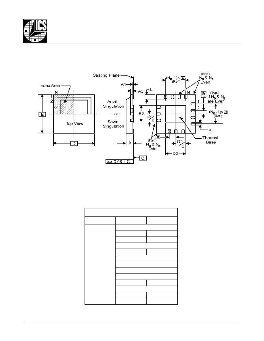
P
ACKAGE
O
UTLINE
- K S
UFFIX
FOR
16 L
EAD
VFQFN
T
ABLE
5. P
ACKAGE
D
IMENSIONS
Reference Document: JEDEC Publication 95, MO-220
N
O
I
T
A
I
R
A
V
C
E
D
E
J
S
R
E
T
E
M
I
L
L
I
M
N
I
S
N
O
I
S
N
E
M
I
D
L
L
A
L
O
B
M
Y
S
M
U
M
I
N
I
M
M
U
M
I
X
A
M
N
6
1
A
0
8
.
0
0
.
1
1
A
0
5
0
.
0
3
A
e
c
n
e
r
e
f
e
R
5
2
.
0
b
8
1
.
0
0
3
.
0
e
C
I
S
A
B
0
5
.
0
N
D
4
N
E
4
D
0
.
3
2
D
5
2
.
0
5
2
.
1
E
0
.
3
2
E
5
2
.
0
5
2
.
1
L
0
3
.
0
0
5
.
0

858020AK
www.icst.com/products/hiperclocks.html
REV. A JULY 9, 2004
12
Integrated
Circuit
Systems, Inc.
ICS858020
L
OW
S
KEW
, 1-
TO
-4
D
IFFERENTIAL
-
TO
-CML F
ANOUT
B
UFFER
PRELIMINARY
T
ABLE
6. O
RDERING
I
NFORMATION
While the information presented herein has been checked for both accuracy and reliability, Integrated Circuit Systems, Incorporated (ICS) assumes no responsibility for either its use
or for infringement of any patents or other rights of third parties, which would result from its use. No other circuits, patents, or licenses are implied. This product is intended for use
in normal commercial and industrial applications. Any other applications such as those requiring high reliability or other extraordinary environmental requirements are not
recommended without additional processing by ICS. ICS reserves the right to change any circuitry or specifications without notice. ICS does not authorize or warrant any ICS product
for use in life support devices or critical medical instruments.
r
e
b
m
u
N
r
e
d
r
O
/
t
r
a
P
g
n
i
k
r
a
M
e
g
a
k
c
a
P
t
n
u
o
C
e
r
u
t
a
r
e
p
m
e
T
K
A
0
2
0
8
5
8
S
C
I
A
0
2
8
N
F
Q
F
V
d
a
e
L
6
1
e
b
u
t
r
e
p
0
2
1
C
∞
5
8
o
t
C
∞
0
4
-
T
K
A
0
2
0
8
5
8
S
C
I
A
0
2
8
l
e
e
R
d
n
a
e
p
a
T
n
o
N
F
Q
F
V
d
a
e
L
6
1
0
0
5
3
C
∞
5
8
o
t
C
∞
0
4
-
The aforementioned trademark. HiPerClockSTM is a trademark of Integrated Circuit Systems, Inc. or its subsidiaries in the United States and/or other countries.