Document Outline
- General Description
- Features
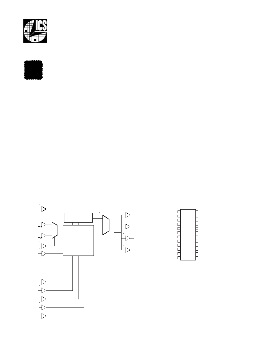
- Block Diagram
- Pin Assignment
- Pin Descriptions
- Pin Characteristics
- PLL Enable Function Table
- PLL Bypass Function Table
- Absolute Maximum Ratings
- Power Supply 3.3V DC Characteristics
- LVCMOS DC Characteristics
- Differential DC Characteristics
- Power Supply 2.5V DC Characteristics
- 3.3V AC Characteristics
- 2.5V AC Characteristics
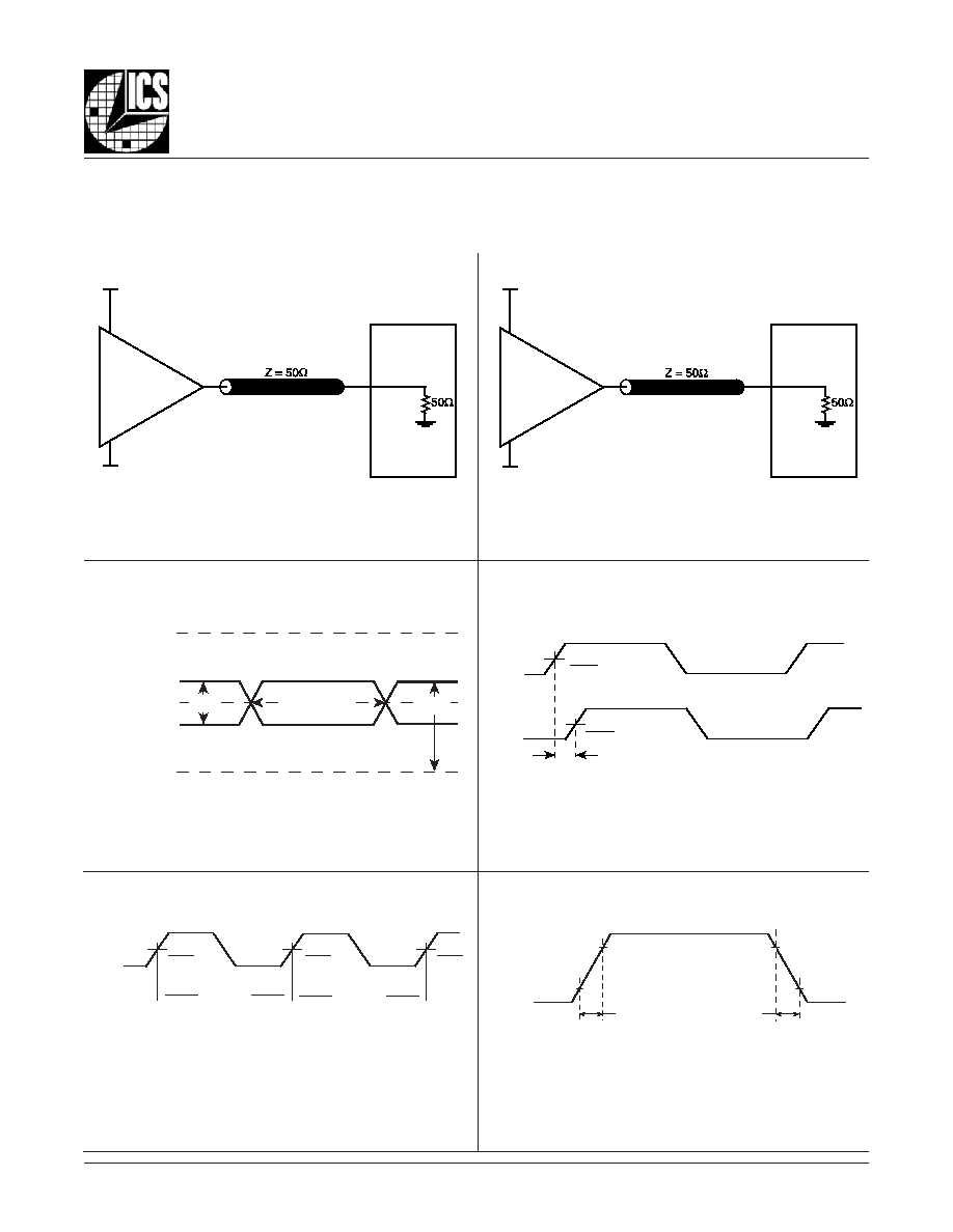
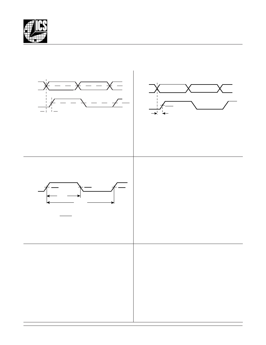
- Parameter Measurement Information
- 3.3V Output Load AC Test Circuit Diagram
- 2.5V Output Load AC Test Circuit Diagram
- Differential Input Level Diagram
- Output Skew Diagram
- Cycle-to-Cycle Jitter Diagram
- Output Rise/Fall Time Diagram
- Static Phase Offset Diagram
- Propagation Delay Diagram
- Output Duty Cycle/Pulse Width/Period Diagram
- Application Information
- Power Supply Filtering Techniques
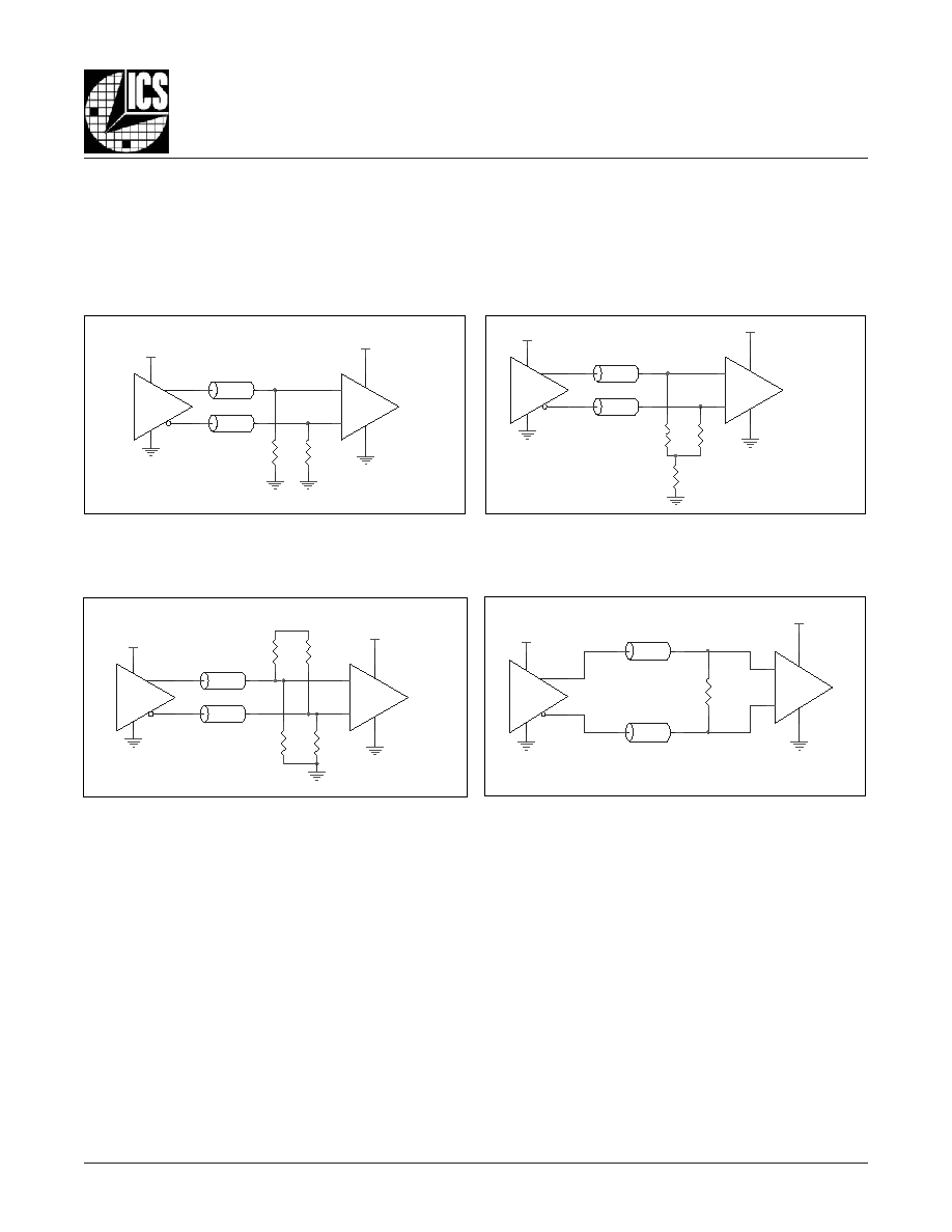
- Wiring the Differential Input to Accept Single Ended Levels
- Differential Clock Input Interface
- HiPerClockS CLK/nCLK Input Driven by ICS HiPerClockS LVHSTL Driver Diagram
- HiPerClockS CLK/nCLK Input Driven by 3.3V LVPECL Driver Diagrams
- HiPerClockS CLK/nCLK Input Driven by 3.3V LVDS Driver Diagram
- Reliability Information
- Transistor Count
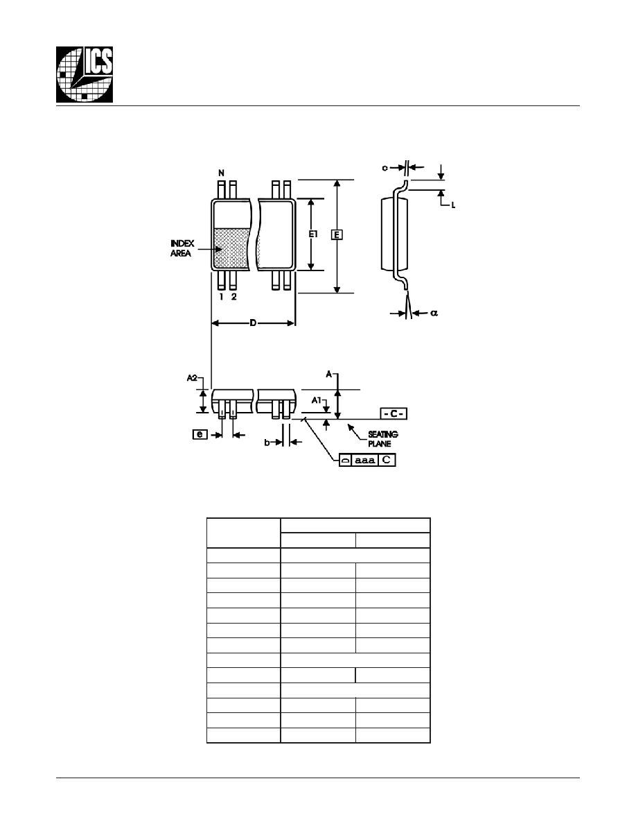
- Package Outline
- Package Dimensions
- Ordering Information
- Revsion History Sheet
87004AG
www.icst.com/products/hiperclocks.html
REV. A JUNE 16, 2004
1
Integrated
Circuit
Systems, Inc.
ICS87004
1:4, D
IFFERENTIAL
-
TO
-LVCMOS/LVTTL
Z
ERO
D
ELAY
C
LOCK
G
ENERATOR
G
ENERAL
D
ESCRIPTION
The ICS87004 is a highly versatile 1:4 Differential-
to-LVCMOS/LVTTL Clock Generator and a mem-
ber of the HiPerClockSTM family of High Perfor-
mance Clock Solutions from ICS. The ICS87004
has two selectable clock inputs. The CLK0, nCLK0
and CLK1, nCLK1 pairs can accept most standard differential
input levels. Internal bias on the nCLK0 and nCLK1 inputs
allows the CLK0 and CLK1 inputs to accept LVCMOS/LVTTL.
The ICS87004 has a fully integrated PLL and can be configured
as zero delay buffer, multiplier or divider and has an input and
output frequency range of 15.625MHz to 250MHz. The refer-
ence divider, feedback divider and output divider are each
programmable, thereby allowing for the following output-to-
input frequency ratios: 8:1, 4:1, 2:1, 1:1, 1:2, 1:4, 1:8. The exter-
nal feedback allows the device to achieve "zero delay" between
the input clock and the output clocks. The PLL_SEL pin can be
used to bypass the PLL for system test and debug purposes. In
bypass mode, the reference clock is routed around the PLL
and into the internal output dividers.
F
EATURES
� 4 LVCMOS/LVTTL outputs, 7
typical output impedance
� Selectable CLK0, nCLK0 or CLK1, nCLK1 clock inputs
� CLKx, nCLKx pairs can accept the following differential
input levels: LVPECL, LVDS, LVHSTL, HCSL, SSTL
� Internal bias on nCLK0 and nCLK1 to support
LVCMOS/LVTTL levels on CLK0 and CLK1 inputs
� Output frequency range: 15.625MHz to 250MHz
� Input frequency range: 15.625MHz to 250MHz
� VCO range: 250MHz to 500MHz
� External feedback for "zero delay" clock regeneration
with configurable frequencies
� Programmable dividers allow for the following output-to-input
frequency ratios: 8:1, 4:1, 2:1, 1:1, 1:2, 1:4, 1:8
� Fully integrated PLL
� Cycle-to-cycle jitter: 45ps (maximum)
� Output skew: 45ps (maximum)
� Static phase offset: 50 � 125ps (3.3V � 5%)
� Full 3.3V or 2.5V operating supply
� 5V tolerant inputs
� Lead-Free package available
� Industrial temperature information available upon request
HiPerClockSTM
ICS
B
LOCK
D
IAGRAM
P
IN
A
SSIGNMENT
24-Lead TSSOP
4.40mm x 7.8mm x 0.92mm
G Package
Top View
PLL_SEL
CLK0
nCLK0
CLK1
nCLK1
CLK_SEL
FB_IN
SEL0
SEL1
SEL2
SEL3
MR
Q0
Q1
Q2
Q3
PLL
8:1, 4:1, 2:1, 1:1,
1:2, 1:4, 1:8
�2, �4, �8, �16,
�32
,
�64, �128
0
1
0
1
GND
Q0
V
DD
o
SEL0
SEL1
SEL2
SEL3
CLK_SEL
V
DD
CLK0
nCLK0
GND
1
2
3
4
5
6
7
8
9
10
11
12
Q1
V
DDO
Q2
GND
Q3
V
DDO
MR
FB_IN
PLL_SEL
CLK1
nCLK1
V
DDA
24
23
22
21
20
19
18
17
16
15
14
13
87004AG
www.icst.com/products/hiperclocks.html
REV. A JUNE 16, 2004
2
Integrated
Circuit
Systems, Inc.
ICS87004
1:4, D
IFFERENTIAL
-
TO
-LVCMOS/LVTTL
Z
ERO
D
ELAY
C
LOCK
G
ENERATOR
T
ABLE
1. P
IN
D
ESCRIPTIONS
T
ABLE
2. P
IN
C
HARACTERISTICS
r
e
b
m
u
N
e
m
a
N
e
p
y
T
n
o
i
t
p
i
r
c
s
e
D
1
2
,
2
1
,
1
D
N
G
r
e
w
o
P
.
d
n
u
o
r
g
y
l
p
p
u
s
r
e
w
o
P
4
2
,
2
2
,
0
2
,
2
,
3
Q
,
0
Q
1
Q
,
2
Q
t
u
p
t
u
O
7
.
s
t
u
p
t
u
o
k
c
o
l
C
.
e
c
n
a
d
e
p
m
i
t
u
p
t
u
o
l
a
c
i
p
y
t
.
s
l
e
v
e
l
e
c
a
f
r
e
t
n
i
L
T
T
V
L
/
S
O
M
C
V
L
3
2
,
9
1
,
3
V
O
D
D
r
e
w
o
P
.
s
n
i
p
y
l
p
p
u
s
t
u
p
t
u
O
7
,
6
,
5
,
4
,
1
L
E
S
,
0
L
E
S
3
L
E
S
,
2
L
E
S
t
u
p
n
I
n
w
o
d
l
l
u
P
.
3
e
l
b
a
T
n
i
s
e
u
l
a
v
r
e
d
i
v
i
d
t
u
p
t
u
o
s
e
n
i
m
r
e
t
e
D
.
s
l
e
v
e
l
e
c
a
f
r
e
t
n
i
L
T
T
V
L
/
S
O
M
C
V
L
8
L
E
S
_
K
L
C
t
u
p
n
I
n
w
o
d
l
l
u
P
.
1
K
L
C
n
,
1
K
L
C
l
a
i
t
n
e
r
e
f
f
i
d
s
t
c
e
l
e
s
,
H
G
I
H
n
e
h
W
.
t
u
p
n
i
t
c
e
l
e
s
k
c
o
l
C
.
0
K
L
C
n
,
0
K
L
C
l
a
i
t
n
e
r
e
f
f
i
d
s
t
c
e
l
e
s
,
W
O
L
n
e
h
W
.
s
l
e
v
e
l
e
c
a
f
r
e
t
n
i
L
T
T
V
L
/
S
O
M
C
V
L
9
V
D
D
r
e
w
o
P
.
n
i
p
y
l
p
p
u
s
e
r
o
C
0
1
0
K
L
C
t
u
p
n
I
n
w
o
d
l
l
u
P
.
t
u
p
n
i
k
c
o
l
c
l
a
i
t
n
e
r
e
f
f
i
d
g
n
i
t
r
e
v
n
i
-
n
o
N
1
1
0
K
L
C
n
t
u
p
n
I
/
p
u
l
l
u
P
n
w
o
d
l
l
u
P
V
.
t
u
p
n
i
k
c
o
l
c
l
a
i
t
n
e
r
e
f
f
i
d
g
n
i
t
r
e
v
n
I
D
D
.
g
n
i
t
a
o
l
f
t
f
e
l
n
e
h
w
t
l
u
a
f
e
d
2
/
3
1
V
A
D
D
r
e
w
o
P
.
n
i
p
y
l
p
p
u
s
g
o
l
a
n
A
4
1
1
K
L
C
n
t
u
p
n
I
/
p
u
l
l
u
P
n
w
o
d
l
l
u
P
V
.
t
u
p
n
i
k
c
o
l
c
l
a
i
t
n
e
r
e
f
f
i
d
g
n
i
t
r
e
v
n
I
D
D
.
g
n
i
t
a
o
l
f
t
f
e
l
n
e
h
w
t
l
u
a
f
e
d
2
/
5
1
1
K
L
C
t
u
p
n
I
n
w
o
d
l
l
u
P
.
t
u
p
n
i
k
c
o
l
c
l
a
i
t
n
e
r
e
f
f
i
d
g
n
i
t
r
e
v
n
i
-
n
o
N
6
1
L
E
S
_
L
L
P
t
u
p
n
I
p
u
l
l
u
P
.
s
r
e
d
i
v
i
d
e
h
t
o
t
t
u
p
n
i
s
a
k
c
o
l
c
e
c
n
e
r
e
f
e
r
d
n
a
L
L
P
e
h
t
n
e
e
w
t
e
b
s
t
c
e
l
e
S
,
H
G
I
H
n
e
h
W
.
)
s
s
a
p
y
B
L
L
P
(
k
c
o
l
c
e
c
n
e
r
e
f
e
r
e
h
t
s
t
c
e
l
e
s
,
W
O
L
n
e
h
W
.
s
l
e
v
e
l
e
c
a
f
r
e
t
n
i
L
T
T
V
L
/
S
O
M
C
V
L
.
)
d
e
l
b
a
n
E
L
L
P
(
L
L
P
s
t
c
e
l
e
s
7
1
N
I
_
B
F
t
u
p
n
I
n
w
o
d
l
l
u
P
g
n
i
t
a
r
e
n
e
g
e
r
r
o
f
r
o
t
c
e
t
e
d
e
s
a
h
p
o
t
t
u
p
n
i
k
c
a
b
d
e
e
f
L
T
T
V
L
/
S
O
M
C
V
L
.
s
t
u
p
t
u
o
e
h
t
f
o
e
n
o
o
t
t
c
e
n
n
o
C
.
"
y
a
l
e
d
o
r
e
z
"
h
t
i
w
s
k
c
o
l
c
.
s
l
e
v
e
l
e
c
a
f
r
e
t
n
i
L
T
T
V
L
/
S
O
M
C
V
L
8
1
R
M
t
u
p
n
I
n
w
o
d
l
l
u
P
e
r
a
s
r
e
d
i
v
i
d
l
a
n
r
e
t
n
i
e
h
t
,
H
G
I
H
c
i
g
o
l
n
e
h
W
.
t
e
s
e
R
r
e
t
s
a
M
H
G
I
H
e
v
i
t
c
A
l
a
n
r
e
t
n
i
e
h
t
,
W
O
L
c
i
g
o
l
n
e
h
W
.
w
o
l
o
g
o
t
s
t
u
p
t
u
o
e
h
t
g
n
i
s
u
a
c
t
e
s
e
r
.
s
l
e
v
e
l
e
c
a
f
r
e
t
n
i
L
T
T
V
L
/
S
O
M
C
V
L
.
d
e
l
b
a
n
e
e
r
a
s
t
u
p
t
u
o
e
h
t
d
n
a
s
r
e
d
i
v
i
d
:
E
T
O
N
p
u
ll
u
P
d
n
a
n
w
o
d
ll
u
P
.
s
e
u
l
a
v
l
a
c
i
p
y
t
r
o
f
,
s
c
i
t
s
i
r
e
t
c
a
r
a
h
C
n
i
P
,
2
e
l
b
a
T
e
e
S
.
s
r
o
t
s
i
s
e
r
t
u
p
n
i
l
a
n
r
e
t
n
i
o
t
r
e
f
e
r
l
o
b
m
y
S
r
e
t
e
m
a
r
a
P
s
n
o
i
t
i
d
n
o
C
t
s
e
T
m
u
m
i
n
i
M
l
a
c
i
p
y
T
m
u
m
i
x
a
M
s
t
i
n
U
C
N
I
e
c
n
a
t
i
c
a
p
a
C
t
u
p
n
I
4
F
p
R
P
U
L
L
U
P
r
o
t
s
i
s
e
R
p
u
ll
u
P
t
u
p
n
I
1
5
K
R
N
W
O
D
L
L
U
P
r
o
t
s
i
s
e
R
n
w
o
d
ll
u
P
t
u
p
n
I
1
5
K
C
D
P
e
c
n
a
t
i
c
a
p
a
C
n
o
i
t
a
p
i
s
s
i
D
r
e
w
o
P
)
t
u
p
t
u
o
r
e
p
(
V
D
D
V
,
A
D
D
V
,
O
D
D
V
5
6
4
.
3
=
3
2
F
p
V
D
D
V
,
A
D
D
V
,
O
D
D
V
5
2
6
.
2
=
7
1
F
p
R
T
U
O
e
c
n
a
d
e
p
m
I
t
u
p
t
u
O
5
7
2
1

87004AG
www.icst.com/products/hiperclocks.html
REV. A JUNE 16, 2004
3
Integrated
Circuit
Systems, Inc.
ICS87004
1:4, D
IFFERENTIAL
-
TO
-LVCMOS/LVTTL
Z
ERO
D
ELAY
C
LOCK
G
ENERATOR
T
ABLE
3A. PLL E
NABLE
F
UNCTION
T
ABLE
s
t
u
p
n
I
s
t
u
p
t
u
O
0
=
L
E
S
_
L
L
P
e
d
o
M
s
s
a
p
y
B
L
L
P
3
L
E
S
2
L
E
S
1
L
E
S
0
L
E
S
3
Q
:
0
Q
0
0
0
0
8
�
0
0
0
1
8
�
0
0
1
0
8
�
0
0
1
1
6
1
�
0
1
0
0
6
1
�
0
1
0
1
6
1
�
0
1
1
0
2
3
�
0
1
1
1
2
3
�
1
0
0
0
4
6
�
1
0
0
1
8
2
1
�
1
0
1
0
4
�
1
0
1
1
4
�
1
1
0
0
8
�
1
1
0
1
2
�
1
1
1
0
4
�
1
1
1
1
2
�
T
ABLE
3B. PLL B
YPASS
F
UNCTION
T
ABLE
s
t
u
p
n
I
s
t
u
p
t
u
O
1
=
L
E
S
_
L
L
P
e
d
o
M
e
l
b
a
n
E
L
L
P
3
L
E
S
2
L
E
S
1
L
E
S
0
L
E
S
)
z
H
M
(
e
g
n
a
R
y
c
n
e
u
q
e
r
F
e
c
n
e
r
e
f
e
R
3
Q
:
0
Q
0
0
0
0
0
5
2
-
5
2
1
1
�
0
0
0
1
5
2
1
-
5
.
2
6
1
�
0
0
1
0
5
.
2
6
-
5
2
.
1
3
1
�
0
0
1
1
5
2
.
1
3
-
5
2
6
.
5
1
1
�
0
1
0
0
0
5
2
-
5
2
1
2
�
0
1
0
1
5
2
1
-
5
.
2
6
2
�
0
1
1
0
5
.
2
6
-
5
2
.
1
3
2
�
0
1
1
1
0
5
2
-
5
2
1
4
�
1
0
0
0
5
2
1
-
5
.
2
6
4
�
1
0
0
1
0
5
2
-
5
2
1
8
�
1
0
1
0
5
2
1
-
5
.
2
6
2
x
1
0
1
1
5
.
2
6
-
5
2
.
1
3
2
x
1
1
0
0
5
2
.
1
3
-
5
2
6
.
5
1
2
x
1
1
0
1
5
.
2
6
-
5
2
.
1
3
4
x
1
1
1
0
5
2
.
1
3
-
5
2
6
.
5
1
4
x
1
1
1
1
5
2
.
1
3
-
5
2
6
.
5
1
8
x

87004AG
www.icst.com/products/hiperclocks.html
REV. A JUNE 16, 2004
4
Integrated
Circuit
Systems, Inc.
ICS87004
1:4, D
IFFERENTIAL
-
TO
-LVCMOS/LVTTL
Z
ERO
D
ELAY
C
LOCK
G
ENERATOR
T
ABLE
4A. P
OWER
S
UPPLY
DC C
HARACTERISTICS
,
V
DD
= V
DDA
= V
DDO
= 3.3V�5%, TA = 0�C
TO
70�C
l
o
b
m
y
S
r
e
t
e
m
a
r
a
P
s
n
o
i
t
i
d
n
o
C
t
s
e
T
m
u
m
i
n
i
M
l
a
c
i
p
y
T
m
u
m
i
x
a
M
s
t
i
n
U
V
D
D
e
g
a
t
l
o
V
y
l
p
p
u
S
e
r
o
C
5
3
1
.
3
3
.
3
5
6
4
.
3
V
V
A
D
D
e
g
a
t
l
o
V
y
l
p
p
u
S
g
o
l
a
n
A
5
3
1
.
3
3
.
3
5
6
4
.
3
V
V
O
D
D
e
g
a
t
l
o
V
y
l
p
p
u
S
t
u
p
t
u
O
5
3
1
.
3
3
.
3
5
6
4
.
3
V
I
D
D
t
n
e
r
r
u
C
y
l
p
p
u
S
r
e
w
o
P
0
0
1
A
m
I
A
D
D
t
n
e
r
r
u
C
y
l
p
p
u
S
g
o
l
a
n
A
6
1
A
m
I
O
D
D
t
n
e
r
r
u
C
y
l
p
p
u
S
t
u
p
t
u
O
6
A
m
T
ABLE
4B. LVCMOS / LVTTL DC C
HARACTERISTICS
,
V
DD
= V
DDA
= V
DDO
= 3.3V�5%
OR
2.5V�5%, TA = 0�C
TO
70�C
A
BSOLUTE
M
AXIMUM
R
ATINGS
Supply Voltage, V
DD
4.6V
Inputs, V
I
-0.5V to V
DD
+ 0.5 V
Outputs, V
O
-0.5V to V
DDO
+ 0.5V
Package Thermal Impedance,
JA
70�C/W (0 lfpm)
Storage Temperature, T
STG
-65�C to 150�C
NOTE: Stresses beyond those listed under Absolute
Maximum Ratings may cause permanent damage to the
device. These ratings are stress specifications only. Functional
operation of product at these conditions or any conditions be-
yond those listed in the
DC Characteristics or AC Character-
istics is not implied. Exposure to absolute maximum rating
conditions for extended periods may affect product reliability.
l
o
b
m
y
S
r
e
t
e
m
a
r
a
P
s
n
o
i
t
i
d
n
o
C
t
s
e
T
m
u
m
i
n
i
M
l
a
c
i
p
y
T
m
u
m
i
x
a
M
s
t
i
n
U
V
H
I
t
u
p
n
I
e
g
a
t
l
o
V
h
g
i
H
,
L
E
S
_
K
L
C
,
L
E
S
_
L
L
P
,
3
L
E
S
,
2
L
E
S
,
1
L
E
S
,
0
L
E
S
R
M
,
N
I
_
B
F
2
V
D
D
3
.
0
+
V
V
L
I
t
u
p
n
I
e
g
a
t
l
o
V
w
o
L
,
L
E
S
_
K
L
C
,
L
E
S
_
L
L
P
,
3
L
E
S
,
2
L
E
S
,
1
L
E
S
,
0
L
E
S
R
M
,
N
I
_
B
F
3
.
0
-
8
.
0
V
I
H
I
t
u
p
n
I
t
n
e
r
r
u
C
h
g
i
H
,
N
I
_
B
F
,
R
M
,
L
E
S
_
K
L
C
3
L
E
S
,
2
L
E
S
,
1
L
E
S
,
0
L
E
S
V
D
D
V
=
N
I
,
V
5
6
4
.
3
=
V
D
D
V
=
N
I
V
5
2
6
.
2
=
0
5
1
A
�
L
E
S
_
L
L
P
V
D
D
V
=
N
I
,
V
5
6
4
.
3
=
V
D
D
V
=
N
I
V
5
2
6
.
2
=
5
A
�
I
L
I
t
u
p
n
I
t
n
e
r
r
u
C
w
o
L
,
N
I
_
B
F
,
R
M
,
L
E
S
_
K
L
C
3
L
E
S
,
2
L
E
S
,
1
L
E
S
,
0
L
E
S
V
D
D
V
,
V
5
6
4
.
3
=
N
I
,
V
0
=
V
D
D
V
,
V
5
2
6
.
2
=
N
I
V
0
=
5
-
A
�
L
E
S
_
L
L
P
V
D
D
V
,
V
5
6
4
.
3
=
N
I
,
V
0
=
V
D
D
V
,
V
5
2
6
.
2
=
N
I
V
0
=
0
5
1
-
A
�
V
H
O
1
E
T
O
N
;
e
g
a
t
l
o
V
h
g
i
H
t
u
p
t
u
O
V
O
D
D
V
5
6
4
.
3
=
6
.
2
V
V
O
D
D
V
5
2
6
.
2
=
8
.
1
V
V
L
O
1
E
T
O
N
;
e
g
a
t
l
o
V
w
o
L
t
u
p
t
u
O
V
O
D
D
V
5
2
6
.
2
r
o
V
5
6
4
.
3
=
5
.
0
V
0
5
h
t
i
w
d
e
t
a
n
i
m
r
e
t
s
t
u
p
t
u
O
:
1
E
T
O
N
V
o
t
O
D
D
,
n
o
i
t
c
e
S
n
o
i
t
a
m
r
o
f
n
I
t
n
e
m
e
r
u
s
a
e
M
r
e
t
e
m
a
r
a
P
e
h
t
n
I
.
2
/
e
e
s
.
s
m
a
r
g
a
i
D
t
i
u
c
r
i
C
t
s
e
T
d
a
o
L
t
u
p
t
u
O
87004AG
www.icst.com/products/hiperclocks.html
REV. A JUNE 16, 2004
5
Integrated
Circuit
Systems, Inc.
ICS87004
1:4, D
IFFERENTIAL
-
TO
-LVCMOS/LVTTL
Z
ERO
D
ELAY
C
LOCK
G
ENERATOR
T
ABLE
4C. D
IFFERENTIAL
DC C
HARACTERISTICS
,
V
DD
= V
DDA
= V
DDO
= 3.3V�5%
OR
2.5V�5%, TA = 0�C
TO
70�C
l
o
b
m
y
S
r
e
t
e
m
a
r
a
P
s
n
o
i
t
i
d
n
o
C
t
s
e
T
m
u
m
i
n
i
M
l
a
c
i
p
y
T
m
u
m
i
x
a
M
s
t
i
n
U
I
H
I
t
n
e
r
r
u
C
h
g
i
H
t
u
p
n
I
1
K
L
C
,
0
K
L
C
V
D
D
V
=
N
I
,
V
5
6
4
.
3
=
V
D
D
V
=
N
I
V
5
2
6
.
2
=
0
5
1
A
�
1
K
L
C
n
,
0
K
L
C
n
V
D
D
V
=
N
I
,
V
5
6
4
.
3
=
V
D
D
V
=
N
I
V
5
2
6
.
2
=
0
5
1
A
�
I
L
I
t
n
e
r
r
u
C
w
o
L
t
u
p
n
I
1
K
L
C
,
0
K
L
C
V
D
D
V
,
V
5
6
4
.
3
=
N
I
,
V
0
=
V
D
D
V
,
V
5
2
6
.
2
=
N
I
V
0
=
5
-
A
�
1
K
L
C
n
,
0
K
L
C
n
V
D
D
V
,
V
5
6
4
.
3
=
N
I
,
V
0
=
V
D
D
V
,
V
5
2
6
.
2
=
N
I
V
0
=
0
5
1
-
A
�
V
P
P
e
g
a
t
l
o
V
t
u
p
n
I
k
a
e
P
-
o
t
-
k
a
e
P
5
1
.
0
3
.
1
V
V
R
M
C
;
e
g
a
t
l
o
V
t
u
p
n
I
e
d
o
M
n
o
m
m
o
C
2
,
1
E
T
O
N
5
.
0
+
D
N
G
V
D
D
5
8
.
0
-
V
s
a
d
e
n
i
f
e
d
s
i
e
g
a
t
l
o
v
e
d
o
m
n
o
m
m
o
C
:
1
E
T
O
N
V
H
I
.
s
i
1
K
L
C
n
,
1
K
L
C
d
n
a
0
K
L
C
n
,
0
K
L
C
r
o
f
e
g
a
t
l
o
v
t
u
p
n
i
m
u
m
i
x
a
m
e
h
t
,
s
n
o
i
t
a
c
il
p
p
a
d
e
d
n
e
e
l
g
n
i
s
r
o
F
:
2
E
T
O
N
V
D
D
.
V
3
.
0
+
T
ABLE
4D. P
OWER
S
UPPLY
DC C
HARACTERISTICS
,
V
DD
= V
DDA
= V
DDO
= 2.5V�5%, TA = 0�C
TO
70�C
l
o
b
m
y
S
r
e
t
e
m
a
r
a
P
s
n
o
i
t
i
d
n
o
C
t
s
e
T
m
u
m
i
n
i
M
l
a
c
i
p
y
T
m
u
m
i
x
a
M
s
t
i
n
U
V
D
D
e
g
a
t
l
o
V
y
l
p
p
u
S
e
r
o
C
5
7
3
.
2
5
.
2
5
2
6
.
2
V
V
A
D
D
e
g
a
t
l
o
V
y
l
p
p
u
S
g
o
l
a
n
A
5
7
3
.
2
5
.
2
5
2
6
.
2
V
V
O
D
D
e
g
a
t
l
o
V
y
l
p
p
u
S
t
u
p
t
u
O
5
7
3
.
2
5
.
2
5
2
6
.
2
V
I
D
D
t
n
e
r
r
u
C
y
l
p
p
u
S
r
e
w
o
P
6
9
A
m
I
A
D
D
t
n
e
r
r
u
C
y
l
p
p
u
S
g
o
l
a
n
A
5
1
A
m
I
O
D
D
t
n
e
r
r
u
C
y
l
p
p
u
S
t
u
p
t
u
O
6
A
m

87004AG
www.icst.com/products/hiperclocks.html
REV. A JUNE 16, 2004
6
Integrated
Circuit
Systems, Inc.
ICS87004
1:4, D
IFFERENTIAL
-
TO
-LVCMOS/LVTTL
Z
ERO
D
ELAY
C
LOCK
G
ENERATOR
T
ABLE
5B. AC C
HARACTERISTICS
,
V
DD
= V
DDA
= V
DDO
= 2.5V�5%, TA = 0�C
TO
70�C
l
o
b
m
y
S
r
e
t
e
m
a
r
a
P
s
n
o
i
t
i
d
n
o
C
t
s
e
T
m
u
m
i
n
i
M
l
a
c
i
p
y
T
m
u
m
i
x
a
M
s
t
i
n
U
f
X
A
M
y
c
n
e
u
q
e
r
F
t
u
p
t
u
O
5
2
6
.
5
1
0
5
2
z
H
M
t
D
P
,
y
a
l
e
D
n
o
i
t
a
g
a
p
o
r
P
1
E
T
O
N
0
K
L
C
n
,
0
K
L
C
1
K
L
C
n
,
1
K
L
C
V
0
=
L
E
S
_
L
L
P
f
2
�
x
Q
,
z
H
M
0
5
2
3
.
5
7
.
6
s
n
)
�
(
t
;
t
e
s
f
f
O
e
s
a
h
P
c
i
t
a
t
S
4
,
2
E
T
O
N
0
K
L
C
n
,
0
K
L
C
1
K
L
C
n
,
1
K
L
C
V
5
.
2
=
L
E
S
_
L
L
P
f
F
E
R
1
�
x
Q
,
z
H
M
7
6
1
5
7
1
-
5
2
-
5
2
1
s
p
t
)
o
(
k
s
;
w
e
k
S
t
u
p
t
u
O
4
,
3
E
T
O
N
0
K
L
C
n
,
0
K
L
C
1
K
L
C
n
,
1
K
L
C
V
0
=
L
E
S
_
L
L
P
0
4
5
4
s
p
t
)
c
c
(
t
ij
4
E
T
O
N
;
r
e
t
t
i
J
e
l
c
y
C
-
o
t
-
e
l
c
y
C
f
T
U
O
z
H
M
0
4
>
5
3
5
4
s
p
t
L
e
m
i
T
k
c
o
L
L
L
P
1
s
m
t
R
t
/
F
e
m
i
T
ll
a
F
/
e
s
i
R
t
u
p
t
u
O
%
0
8
o
t
%
0
2
0
0
4
0
0
7
s
p
c
d
o
e
l
c
y
C
y
t
u
D
t
u
p
t
u
O
4
4
0
5
6
5
%
t
a
t
u
p
t
u
o
e
h
t
o
t
t
n
i
o
p
g
n
i
s
s
o
r
c
t
u
p
n
i
l
a
i
t
n
e
r
e
f
f
i
d
e
h
t
m
o
r
f
d
e
r
u
s
a
e
M
:
1
E
T
O
N
V
O
D
D
.
2
/
e
h
t
d
n
a
k
c
o
l
c
e
c
n
e
r
e
f
e
r
t
u
p
n
i
e
h
t
n
e
e
w
t
e
b
e
c
n
e
r
e
f
f
i
d
e
m
i
t
e
h
t
s
a
d
e
n
i
f
e
D
:
2
E
T
O
N
l
a
n
g
i
s
t
u
p
n
i
k
c
a
b
d
e
e
f
e
g
a
r
e
v
a
.
e
l
b
a
t
s
s
i
y
c
n
e
u
q
e
r
f
e
c
n
e
r
e
f
e
r
t
u
p
n
i
e
h
t
d
n
a
d
e
k
c
o
l
s
i
L
L
P
e
h
t
n
e
h
w
.
s
n
o
i
t
i
d
n
o
c
d
a
o
l
l
a
u
q
e
h
t
i
w
d
n
a
s
e
g
a
t
l
o
v
y
l
p
p
u
s
e
m
a
s
e
h
t
t
a
s
t
u
p
t
u
o
n
e
e
w
t
e
b
w
e
k
s
s
a
d
e
n
i
f
e
D
:
3
E
T
O
N
V
t
a
d
e
r
u
s
a
e
M
O
D
D
.
2
/
.
5
6
d
r
a
d
n
a
t
S
C
E
D
E
J
h
t
i
w
e
c
n
a
d
r
o
c
c
a
n
i
d
e
n
i
f
e
d
s
i
r
e
t
e
m
a
r
a
p
s
i
h
T
:
4
E
T
O
N
T
ABLE
5A. AC C
HARACTERISTICS
,
V
DD
= V
DDA
= V
DDO
= 3.3V�5%, TA = 0�C
TO
70�C
l
o
b
m
y
S
r
e
t
e
m
a
r
a
P
s
n
o
i
t
i
d
n
o
C
t
s
e
T
m
u
m
i
n
i
M
l
a
c
i
p
y
T
m
u
m
i
x
a
M
s
t
i
n
U
f
X
A
M
y
c
n
e
u
q
e
r
F
t
u
p
t
u
O
5
2
6
.
5
1
0
5
2
z
H
M
t
D
P
,
y
a
l
e
D
n
o
i
t
a
g
a
p
o
r
P
1
E
T
O
N
0
K
L
C
n
,
0
K
L
C
1
K
L
C
n
,
1
K
L
C
V
0
=
L
E
S
_
L
L
P
f
2
�
x
Q
,
z
H
M
0
5
2
5
6
s
n
)
�
(
t
;
t
e
s
f
f
O
e
s
a
h
P
c
i
t
a
t
S
4
,
2
E
T
O
N
0
K
L
C
n
,
0
K
L
C
1
K
L
C
n
,
1
K
L
C
V
3
.
3
=
L
E
S
_
L
L
P
f
F
E
R
1
�
x
Q
,
z
H
M
7
6
1
5
7
-
0
5
5
7
1
s
p
t
)
o
(
k
s
;
w
e
k
S
t
u
p
t
u
O
4
,
3
E
T
O
N
0
K
L
C
n
,
0
K
L
C
1
K
L
C
n
,
1
K
L
C
V
0
=
L
E
S
_
L
L
P
0
4
0
5
s
p
t
)
c
c
(
t
ij
4
E
T
O
N
;
r
e
t
t
i
J
e
l
c
y
C
-
o
t
-
e
l
c
y
C
f
T
U
O
z
H
M
0
4
>
0
3
5
4
s
p
t
L
e
m
i
T
k
c
o
L
L
L
P
1
s
m
t
R
t
/
F
e
m
i
T
ll
a
F
/
e
s
i
R
t
u
p
t
u
O
%
0
8
o
t
%
0
2
0
0
4
0
0
8
s
p
c
d
o
e
l
c
y
C
y
t
u
D
t
u
p
t
u
O
0
4
0
5
0
6
%
t
a
t
u
p
t
u
o
e
h
t
o
t
t
n
i
o
p
g
n
i
s
s
o
r
c
t
u
p
n
i
l
a
i
t
n
e
r
e
f
f
i
d
e
h
t
m
o
r
f
d
e
r
u
s
a
e
M
:
1
E
T
O
N
V
O
D
D
.
2
/
e
h
t
d
n
a
k
c
o
l
c
e
c
n
e
r
e
f
e
r
t
u
p
n
i
e
h
t
n
e
e
w
t
e
b
e
c
n
e
r
e
f
f
i
d
e
m
i
t
e
h
t
s
a
d
e
n
i
f
e
D
:
2
E
T
O
N
l
a
n
g
i
s
t
u
p
n
i
k
c
a
b
d
e
e
f
e
g
a
r
e
v
a
.
e
l
b
a
t
s
s
i
y
c
n
e
u
q
e
r
f
e
c
n
e
r
e
f
e
r
t
u
p
n
i
e
h
t
d
n
a
d
e
k
c
o
l
s
i
L
L
P
e
h
t
n
e
h
w
.
s
n
o
i
t
i
d
n
o
c
d
a
o
l
l
a
u
q
e
h
t
i
w
d
n
a
s
e
g
a
t
l
o
v
y
l
p
p
u
s
e
m
a
s
e
h
t
t
a
s
t
u
p
t
u
o
n
e
e
w
t
e
b
w
e
k
s
s
a
d
e
n
i
f
e
D
:
3
E
T
O
N
V
t
a
d
e
r
u
s
a
e
M
O
D
D
.
2
/
.
5
6
d
r
a
d
n
a
t
S
C
E
D
E
J
h
t
i
w
e
c
n
a
d
r
o
c
c
a
n
i
d
e
n
i
f
e
d
s
i
r
e
t
e
m
a
r
a
p
s
i
h
T
:
4
E
T
O
N
87004AG
www.icst.com/products/hiperclocks.html
REV. A JUNE 16, 2004
7
Integrated
Circuit
Systems, Inc.
ICS87004
1:4, D
IFFERENTIAL
-
TO
-LVCMOS/LVTTL
Z
ERO
D
ELAY
C
LOCK
G
ENERATOR
D
IFFERENTIAL
I
NPUT
L
EVEL
2.5V O
UTPUT
L
OAD
AC T
EST
C
IRCUIT
3.3V O
UTPUT
L
OAD
AC T
EST
C
IRCUIT
SCOPE
Qx
LVCMOS
1.65V�5%
-1.65V�5%
O
UTPUT
S
KEW
C
YCLE
-
TO
-C
YCLE
J
ITTER
O
UTPUT
R
ISE
/F
ALL
T
IME
SCOPE
Qx
LVCMOS
1.25V�5%
-1.25V�5%
P
ARAMETER
M
EASUREMENT
I
NFORMATION
V
CMR
Cross Points
V
PP
GND
CLK0, CLK1
nCLK0, nCLK1
V
DD
t
jit(cc) =
t
cycle n �
t
cycle n+1
1000 Cycles
Q0:Q3
V
DDO
2
V
DDO
2
V
DDO
2
t
cycle n
t
cycle n+1
tsk(o)
V
DDO
2
V
DDO
2
Qy
Qx
Clock
Outputs
20%
80%
80%
20%
t
R
t
F
V
DD
,
V
DDA
, V
DDO
GND
V
DD
,
V
DDA
, V
DDO
GND
87004AG
www.icst.com/products/hiperclocks.html
REV. A JUNE 16, 2004
8
Integrated
Circuit
Systems, Inc.
ICS87004
1:4, D
IFFERENTIAL
-
TO
-LVCMOS/LVTTL
Z
ERO
D
ELAY
C
LOCK
G
ENERATOR
O
UTPUT
D
UTY
C
YCLE
/P
ULSE
W
IDTH
/P
ERIOD
P
ROPAGATION
D
ELAY
S
TATIC
P
HASE
O
FFSET
Q0:Q3
t
PD
V
DDO
2
(where
t(�) is any random sample, and t(�)
mean
is the average
of the sampled cycles measured on controlled edges)
t(�)
mean
= Static Phase Offset
t(�)
V
OH
V
OL
V
OH
V
OL
V
DDO
2
nCLK0,
nCLK1
CLK0,
CLK1
FB_IN
t
PW
t
PERIOD
V
DDO
2
V
DDO
2
V
DDO
2
t
PW
t
PERIOD
odc =
Q0:Q3
nCLK0,
nCLK1
CLK0,
CLK1

87004AG
www.icst.com/products/hiperclocks.html
REV. A JUNE 16, 2004
9
Integrated
Circuit
Systems, Inc.
ICS87004
1:4, D
IFFERENTIAL
-
TO
-LVCMOS/LVTTL
Z
ERO
D
ELAY
C
LOCK
G
ENERATOR
A
PPLICATION
I
NFORMATION
As in any high speed analog circuitry, the power supply pins
are vulnerable to random noise. The ICS87004 provides sepa-
r a t e p o w e r s u p p l i e s t o i s o l a t e a n y h i g h s w i t c h i n g
noise from the outputs to the internal PLL. V
DD
, V
DDA
, and V
DDO
should be individually connected to the power supply
plane through vias, and bypass capacitors should be
used for each pin. To achieve optimum jitter performance,
power supply isolation is required.
Figure 1 illustrates how
a 10
resistor along with a 10�F and a .01�F bypass
capacitor should be connected to each V
DDA
.
P
OWER
S
UPPLY
F
ILTERING
T
ECHNIQUES
F
IGURE
1. P
OWER
S
UPPLY
F
ILTERING
10
V
DDA
10
�F
.01
�F
3.3V
.01
�F
V
DD
Figure 2 shows how the differential input can be wired to accept
single ended levels. The reference voltage V_REF = V
DD
/2 is
generated by the bias resistors R1, R2 and C1. This bias circuit
should be located as close as possible to the input pin. The ratio
F
IGURE
2. S
INGLE
E
NDED
S
IGNAL
D
RIVING
D
IFFERENTIAL
I
NPUT
W
IRING
THE
D
IFFERENTIAL
I
NPUT
TO
A
CCEPT
S
INGLE
E
NDED
L
EVELS
of R1 and R2 might need to be adjusted to position the V_REF in
the center of the input voltage swing. For example, if the input
clock swing is only 2.5V and V
DD
= 3.3V, V_REF should be 1.25V
and R2/R1 = 0.609.
V_REF
R1
1K
C1
0.1u
R2
1K
Single Ended Clock Input
CLKx
nCLKx
VDD
87004AG
www.icst.com/products/hiperclocks.html
REV. A JUNE 16, 2004
10
Integrated
Circuit
Systems, Inc.
ICS87004
1:4, D
IFFERENTIAL
-
TO
-LVCMOS/LVTTL
Z
ERO
D
ELAY
C
LOCK
G
ENERATOR
F
IGURE
3C. H
I
P
ER
C
LOCK
S CLK/
N
CLK I
NPUT
D
RIVEN
BY
3.3V LVPECL D
RIVER
F
IGURE
3B. H
I
P
ER
C
LOCK
S CLK/
N
CLK I
NPUT
D
RIVEN
BY
3.3V LVPECL D
RIVER
F
IGURE
3D. H
I
P
ER
C
LOCK
S CLK/
N
CLK I
NPUT
D
RIVEN
BY
3.3V LVDS D
RIVER
3.3V
R1
50
R3
50
Zo = 50 Ohm
LVPECL
Zo = 50 Ohm
HiPerClockS
CLK
nCLK
3.3V
Input
R2
50
Zo = 50 Ohm
Input
HiPerClockS
CLK
nCLK
3.3V
R3
125
R2
84
Zo = 50 Ohm
3.3V
R4
125
LVPECL
R1
84
3.3V
D
IFFERENTIAL
C
LOCK
I
NPUT
I
NTERFACE
The CLK /nCLK accepts LVDS, LVPECL, LVHSTL, SSTL, HCSL
and other differential signals. Both V
SWING
and V
OH
must meet the
V
PP
and V
CMR
input requirements. Figures 3A to 3D show inter-
face examples for the HiPerClockS CLK/nCLK input driven by
the most common driver types. The input interfaces suggested
F
IGURE
3A. H
I
P
ER
C
LOCK
S CLK/
N
CLK I
NPUT
D
RIVEN
BY
ICS H
I
P
ER
C
LOCK
S LVHSTL D
RIVER
here are examples only. Please consult with the vendor of the
driver component to confirm the driver termination requirements.
For example in
Figure 3A, the input termination applies for ICS
HiPerClockS LVHSTL drivers. If you are using an LVHSTL driver
from another vendor, use their termination recommendation.
1.8V
R2
50
Input
LVHSTL Driver
ICS
HiPerClockS
R1
50
LVHSTL
3.3V
Zo = 50 Ohm
Zo = 50 Ohm
HiPerClockS
CLK
nCLK
Zo = 50 Ohm
R1
100
3.3V
LVDS_Driv er
Zo = 50 Ohm
Receiv er
CLK
nCLK
3.3V

87004AG
www.icst.com/products/hiperclocks.html
REV. A JUNE 16, 2004
11
Integrated
Circuit
Systems, Inc.
ICS87004
1:4, D
IFFERENTIAL
-
TO
-LVCMOS/LVTTL
Z
ERO
D
ELAY
C
LOCK
G
ENERATOR
R
ELIABILITY
I
NFORMATION
T
RANSISTOR
C
OUNT
The transistor count for ICS87004 is: 2578
T
ABLE
6.
JA
VS
. A
IR
F
LOW
T
ABLE
FOR
24 L
EAD
TSSOP
JA
by Velocity (Linear Feet per Minute)
0
200
500
Multi-Layer PCB, JEDEC Standard Test Boards
70�C/W
63�C/W
60�C/W
NOTE: Most modern PCB designs use multi-layered boards. The data in the second row pertains to most designs.
87004AG
www.icst.com/products/hiperclocks.html
REV. A JUNE 16, 2004
12
Integrated
Circuit
Systems, Inc.
ICS87004
1:4, D
IFFERENTIAL
-
TO
-LVCMOS/LVTTL
Z
ERO
D
ELAY
C
LOCK
G
ENERATOR
P
ACKAGE
O
UTLINE
- G S
UFFIX
FOR
24 L
EAD
TSSOP
T
ABLE
7. P
ACKAGE
D
IMENSIONS
Reference Document: JEDEC Publication 95, MO-153
L
O
B
M
Y
S
s
r
e
t
e
m
i
l
l
i
M
m
u
m
i
n
i
M
m
u
m
i
x
a
M
N
4
2
A
-
-
0
2
.
1
1
A
5
0
.
0
5
1
.
0
2
A
0
8
.
0
5
0
.
1
b
9
1
.
0
0
3
.
0
c
9
0
.
0
0
2
.
0
D
0
7
.
7
0
9
.
7
E
C
I
S
A
B
0
4
.
6
1
E
0
3
.
4
0
5
.
4
e
C
I
S
A
B
5
6
.
0
L
5
4
.
0
5
7
.
0
�
0
�
8
a
a
a
-
-
0
1
.
0

87004AG
www.icst.com/products/hiperclocks.html
REV. A JUNE 16, 2004
13
Integrated
Circuit
Systems, Inc.
ICS87004
1:4, D
IFFERENTIAL
-
TO
-LVCMOS/LVTTL
Z
ERO
D
ELAY
C
LOCK
G
ENERATOR
T
ABLE
8. O
RDERING
I
NFORMATION
While the information presented herein has been checked for both accuracy and reliability, Integrated Circuit Systems, Incorporated (ICS) assumes no responsibility for either its use or
for infringement of any patents or other rights of third parties, which would result from its use. No other circuits, patents, or licenses are implied. This product is intended for use in normal
commercial applications. Any other applications such as those requiring extended temperature range, high reliability, or other extraordinary environmental requirements are not recom-
mended without additional processing by ICS. ICS reserves the right to change any circuitry or specifications without notice. ICS does not authorize or warrant any ICS product for use
in life support devices or critical medical instruments.
r
e
b
m
u
N
r
e
d
r
O
/
t
r
a
P
g
n
i
k
r
a
M
e
g
a
k
c
a
P
t
n
u
o
C
e
r
u
t
a
r
e
p
m
e
T
G
A
4
0
0
7
8
S
C
I
G
A
4
0
0
7
8
S
C
I
P
O
S
S
T
d
a
e
L
4
2
e
b
u
t
r
e
p
0
6
C
�
0
7
o
t
C
�
0
T
G
A
4
0
0
7
8
S
C
I
G
A
4
0
0
7
8
S
C
I
l
e
e
R
d
n
a
e
p
a
T
n
o
P
O
S
S
T
d
a
e
L
4
2
0
0
5
2
C
�
0
7
o
t
C
�
0
G
A
4
0
0
7
8
S
C
I
G
A
4
0
0
7
8
S
C
I
P
O
S
S
T
"
e
e
r
F
d
a
e
L
"
d
a
e
L
4
2
e
b
u
t
r
e
p
0
6
C
�
0
7
o
t
C
�
0
T
G
A
4
0
0
7
8
S
C
I
G
A
4
0
0
7
8
S
C
I
l
e
e
R
d
n
a
e
p
a
T
n
o
P
O
S
S
T
"
e
e
r
F
d
a
e
L
"
d
a
e
L
4
2
0
0
5
2
C
�
0
7
o
t
C
�
0
The aforementioned trademark, HiPerClockSTM is a trademark of Integrated Circuit Systems, Inc. or its subsidiaries in the United States and/or other countries.
87004AG
www.icst.com/products/hiperclocks.html
REV. A JUNE 16, 2004
14
Integrated
Circuit
Systems, Inc.
ICS87004
1:4, D
IFFERENTIAL
-
TO
-LVCMOS/LVTTL
Z
ERO
D
ELAY
C
LOCK
G
ENERATOR
T
E
E
H
S
Y
R
O
T
S
I
H
N
O
I
S
I
V
E
R
v
e
R
e
l
b
a
T
e
g
a
P
e
g
n
a
h
C
f
o
n
o
i
t
p
i
r
c
s
e
D
e
t
a
D
A
8
T
3
1
.
r
e
b
m
u
n
t
r
a
p
"
e
e
r
F
-
d
a
e
L
"
d
e
d
d
a
-
e
l
b
a
t
n
o
i
t
a
m
r
o
f
n
I
g
n
i
r
e
d
r
O
4
0
/
6
1
/
6