Document Outline
- General Description
- Features
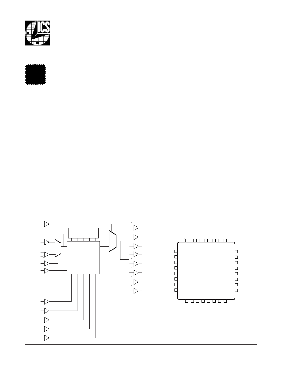
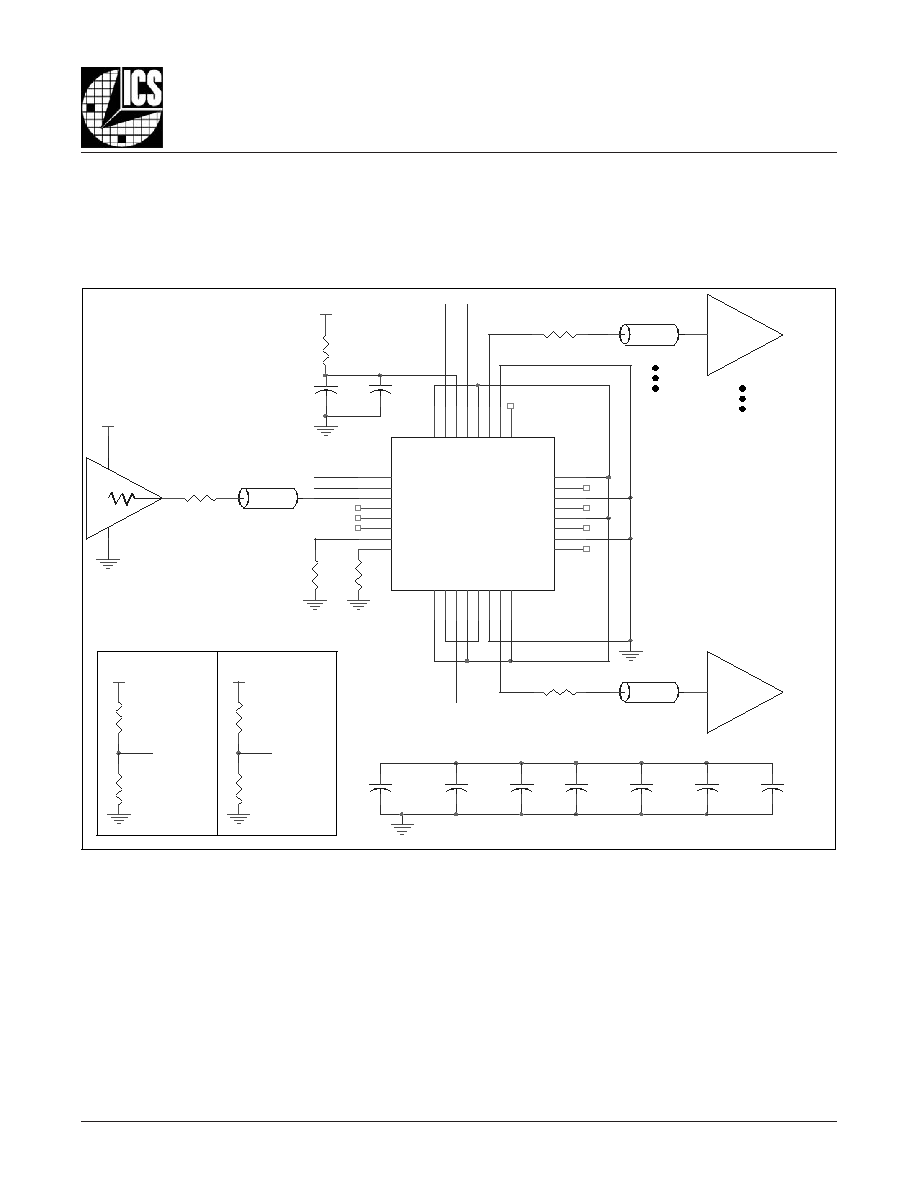
- Block Diagram
- Pin Assignment
- Pin Descriptions
- Pin Characteristics
- PLL Enable Function Table
- PLL Bypass Function Table
- Absolute Maximum Ratings
- Power Supply 3.3V DC Characteristics
- LVCMOS 3.3V DC Characteristics
- Differential 3.3V DC Characteristics
- 3.3V AC Characteristics
- Power Supply 2.5V DC Characteristics
- LVCMOS 2.5V DC Characteristics
- Differential 2.5V DC Characteristics
- 2.5V AC Characteristics
- Parameter Measurement Information
- 3.3V Output Load AC Test Circuit Diagram
- 2.5V Output Load AC Test Circuit Diagram
- Differential Input Level Diagram
- Output Skew Diagram
- Cycle-to-Cycle Jitter Diagram
- Output Rise/Fall Time Diagram
- Phase Jitter & Static Phase Offset Diagram
- Propagation Delay
- tPW, odc & tPeriod Diagram
- Application Information
- Power Supply Filtering Techniques
- Wiring the Differential Input to Accept Single Ended Levels
- Single Ended Signal Driving Differential Input Diagram
- Differential Clock Input Interface
- HiPerClockS CLK/nCLK Input Driven by ICS HiPerClockS LVHSTL Driver Diagram
- HiPerClockS CLK/nCLK Input Driven by LVPECL Driver Diagrams
- HiPerClockS CLK/nCLK Input Driven by LVDS Driver Diagram
- Layout Guideline
- LVCMOS Clock Generator Schematic Example
- Power & Grounding
- Clock Traces & Termiantion
- PCB Board Layout
- Reliability Information
- Tansistor Count
- Package Outline
- Package Dimensions
- Ordering Information
8705BY
www.icst.com/products/hiperclocks.html
REV. G JUNE 16, 2004
1
Integrated
Circuit
Systems, Inc.
ICS8705
Z
ERO
D
ELAY
, D
IFFERENTIAL
-
TO
-LVCMOS/LVTTL
C
LOCK
G
ENERATOR
G
ENERAL
D
ESCRIPTION
The ICS8705 is a highly versatile 1:8 Differen-
tial-to-LVCMOS/LVTTL Clock Generator and a
member of the HiPerClockSTM family of High Per-
formance Clock Solutions from ICS. The ICS8705
has two selectable clock inputs. The CLK1,
nCLK1 pair can accept most standard differential input lev-
els. The single ended CLK0 input accepts LVCMOS or LVTTL
input levels.The ICS8705 has a fully integrated PLL and can
be configured as zero delay buffer, multiplier or divider and
has an input and output frequency range of 15.625MHz to
250MHz. The reference divider, feedback divider and output
divider are each programmable, thereby allowing for the fol-
lowing output-to-input frequency ratios: 8:1, 4:1, 2:1, 1:1, 1:2,
1:4, 1:8. The external feedback allows the device to achieve
"zero delay" between the input clock and the output clocks.
The PLL_SEL pin can be used to bypass the PLL for system
test and debug purposes. In bypass mode, the reference clock
is routed around the PLL and into the internal output dividers.
F
EATURES
� 8 LVCMOS/LVTTL outputs, 7
typical output impedance
� Selectable CLK1, nCLK1 or LVCMOS/LVTTL clock inputs
� CLK1, nCLK1 pair can accept the following differential
input levels: LVPECL, LVDS, LVHSTL, HCSL, SSTL
� CLK0 input accepts LVCMOS or LVTTL input levels
� Output frequency range: 15.625MHz to 250MHz
� Input frequency range: 15.625MHz to 250MHz
� VCO range: 250MHz to 500MHz
� External feedback for "zero delay" clock regeneration
with configurable frequencies
� Programmable dividers allow for the following output-to-input
frequency ratios: 8:1, 4:1, 2:1, 1:1, 1:2, 1:4, 1:8
� Fully integrated PLL
� Cycle-to-cycle jitter: 45ps (maximum)
� Output skew: CLK0, 65ps (maximum)
CLK1, nCLK1, 55ps (maximum)
� Static Phase Offset: 25 �125ps (maximum), CLK0
� Full 3.3V or 2.5V operating supply
� Lead-Free package available
� Industrial temperature information available upon request
HiPerClockSTM
ICS
B
LOCK
D
IAGRAM
P
IN
A
SSIGNMENT
32 31 30 29 28 27 26 25
9 10 11 12 13 14 15 16
1
2
3
4
5
6
7
8
24
23
22
21
20
19
18
17
32-Lead LQFP
7mm x 7mm x 1.4 mm
Y Package
Top View
V
DDO
Q5
GND
Q4
V
DDO
Q3
GND
Q2
SEL0
SEL1
CLK0
nc
CLK1
nCLK1
CLK_SEL
MR
V
DDO
Q1
GND
Q0
V
DDO
SEL2
FB_IN
V
DD
Q6
GND
Q7
V
DDO
SEL3
V
DDA
PLL_SEL
V
DD
ICS8705
PLL_SEL
CLK0
CLK1
nCLK1
CLK_SEL
FB_IN
SEL0
SEL1
SEL2
SEL3
MR
0
1
Q0
Q1
Q2
Q3
Q4
Q5
Q6
Q7
PLL
8:1, 4:1, 2:1, 1:1,
1:2, 1:4, 1:8
�2, �4, �8, �16,
�32
,
�64, �128
0
1
8705BY
www.icst.com/products/hiperclocks.html
REV. G JUNE 16, 2004
2
Integrated
Circuit
Systems, Inc.
ICS8705
Z
ERO
D
ELAY
, D
IFFERENTIAL
-
TO
-LVCMOS/LVTTL
C
LOCK
G
ENERATOR
T
ABLE
1. P
IN
D
ESCRIPTIONS
T
ABLE
2. P
IN
C
HARACTERISTICS
r
e
b
m
u
N
e
m
a
N
e
p
y
T
n
o
i
t
p
i
r
c
s
e
D
1
1
,
2
,
1
,
1
L
E
S
,
0
L
E
S
2
L
E
S
t
u
p
n
I
n
w
o
d
ll
u
P
.
3
e
l
b
a
T
n
i
s
e
u
l
a
v
r
e
d
i
v
i
d
t
u
p
t
u
o
s
e
n
i
m
r
e
t
e
D
.
s
l
e
v
e
l
e
c
a
f
r
e
t
n
i
L
T
T
V
L
/
S
O
M
C
V
L
3
0
K
L
C
t
u
p
n
I
n
w
o
d
ll
u
P
.
s
l
e
v
e
l
e
c
a
f
r
e
t
n
i
L
T
T
V
L
/
S
O
M
C
V
L
.
t
u
p
n
i
k
c
o
l
C
4
c
n
.
t
c
e
n
n
o
c
o
N
5
1
K
L
C
t
u
p
n
I
n
w
o
d
ll
u
P
.
t
u
p
n
i
k
c
o
l
c
l
a
i
t
n
e
r
e
f
f
i
d
g
n
i
t
r
e
v
n
i
-
n
o
N
6
1
K
L
C
n
t
u
p
n
I
p
u
ll
u
P
.
t
u
p
n
i
k
c
o
l
c
l
a
i
t
n
e
r
e
f
f
i
d
g
n
i
t
r
e
v
n
I
7
L
E
S
_
K
L
C
t
u
p
n
I
n
w
o
d
ll
u
P
.
1
K
L
C
n
,
1
K
L
C
l
a
i
t
n
e
r
e
f
f
i
d
s
t
c
e
l
e
s
,
H
G
I
H
n
e
h
W
.
t
u
p
n
i
t
c
e
l
e
s
k
c
o
l
C
.
0
K
L
C
S
O
M
C
V
L
s
t
c
e
l
e
s
,
W
O
L
n
e
h
W
.
s
l
e
v
e
l
e
c
a
f
r
e
t
n
i
L
T
T
V
L
/
S
O
M
C
V
L
8
R
M
t
u
p
n
I
n
w
o
d
ll
u
P
e
r
a
s
r
e
d
i
v
i
d
l
a
n
r
e
t
n
i
e
h
t
,
H
G
I
H
c
i
g
o
l
n
e
h
W
.
t
e
s
e
R
r
e
t
s
a
M
H
G
I
H
e
v
i
t
c
A
l
a
n
r
e
t
n
i
e
h
t
,
W
O
L
c
i
g
o
l
n
e
h
W
.
w
o
l
o
g
o
t
s
t
u
p
t
u
o
e
h
t
g
n
i
s
u
a
c
t
e
s
e
r
.
s
l
e
v
e
l
e
c
a
f
r
e
t
n
i
L
T
T
V
L
/
S
O
M
C
V
L
.
d
e
l
b
a
n
e
e
r
a
s
t
u
p
t
u
o
e
h
t
d
n
a
s
r
e
d
i
v
i
d
2
3
,
9
V
D
D
r
e
w
o
P
.
s
n
i
p
y
l
p
p
u
s
e
r
o
C
0
1
N
I
_
B
F
t
u
p
n
I
n
w
o
d
ll
u
P
g
n
i
t
a
r
e
n
e
g
e
r
r
o
f
r
o
t
c
e
t
e
d
e
s
a
h
p
o
t
t
u
p
n
i
k
c
a
b
d
e
e
f
L
T
T
V
L
/
S
O
M
C
V
L
.
s
t
u
p
t
u
o
e
h
t
f
o
e
n
o
o
t
t
c
e
n
n
o
C
.
"
y
a
l
e
d
o
r
e
z
"
h
t
i
w
s
k
c
o
l
c
.
s
l
e
v
e
l
e
c
a
f
r
e
t
n
i
L
T
T
V
L
/
S
O
M
C
V
L
,
0
2
,
6
1
,
2
1
8
2
,
4
2
V
O
D
D
r
e
w
o
P
.
s
n
i
p
y
l
p
p
u
s
t
u
p
t
u
O
,
7
1
,
5
1
,
3
1
,
3
2
,
1
2
,
9
1
7
2
,
5
2
,
2
Q
,
1
Q
,
0
Q
,
5
Q
,
4
Q
,
3
Q
7
Q
,
6
Q
t
u
p
t
u
O
7
.
t
u
p
t
u
o
k
c
o
l
C
.
e
c
n
a
d
e
p
m
i
t
u
p
t
u
o
l
a
c
i
p
y
t
.
s
l
e
v
e
l
e
c
a
f
r
e
t
n
i
L
T
T
V
L
/
S
O
M
C
V
L
6
2
,
2
2
,
8
1
,
4
1
D
N
G
r
e
w
o
P
.
d
n
u
o
r
g
y
l
p
p
u
s
r
e
w
o
P
9
2
3
L
E
S
t
u
p
n
I
n
w
o
d
ll
u
P
.
3
e
l
b
a
T
n
i
s
e
u
l
a
v
r
e
d
i
v
i
d
t
u
p
t
u
o
s
e
n
i
m
r
e
t
e
D
.
s
l
e
v
e
l
e
c
a
f
r
e
t
n
i
L
T
T
V
L
/
S
O
M
C
V
L
0
3
V
A
D
D
r
e
w
o
P
.
n
i
p
y
l
p
p
u
s
g
o
l
a
n
A
1
3
L
E
S
_
L
L
P
t
u
p
n
I
p
u
ll
u
P
.
s
r
e
d
i
v
i
d
e
h
t
o
t
t
u
p
n
i
s
a
k
c
o
l
c
e
c
n
e
r
e
f
e
r
d
n
a
L
L
P
e
h
t
n
e
e
w
t
e
b
s
t
c
e
l
e
S
,
H
G
I
H
n
e
h
W
.
)
s
s
a
p
y
B
L
L
P
(
k
c
o
l
c
e
c
n
e
r
e
f
e
r
e
h
t
s
t
c
e
l
e
s
,
W
O
L
n
e
h
W
.
s
l
e
v
e
l
e
c
a
f
r
e
t
n
i
L
T
T
V
L
/
S
O
M
C
V
L
.
)
d
e
l
b
a
n
E
L
L
P
(
L
L
P
s
t
c
e
l
e
s
:
E
T
O
N
p
u
ll
u
P
d
n
a
n
w
o
d
ll
u
P
.
s
e
u
l
a
v
l
a
c
i
p
y
t
r
o
f
,
s
c
i
t
s
i
r
e
t
c
a
r
a
h
C
n
i
P
,
2
e
l
b
a
T
e
e
S
.
s
r
o
t
s
i
s
e
r
t
u
p
n
i
l
a
n
r
e
t
n
i
o
t
r
e
f
e
r
l
o
b
m
y
S
r
e
t
e
m
a
r
a
P
s
n
o
i
t
i
d
n
o
C
t
s
e
T
m
u
m
i
n
i
M
l
a
c
i
p
y
T
m
u
m
i
x
a
M
s
t
i
n
U
C
N
I
e
c
n
a
t
i
c
a
p
a
C
t
u
p
n
I
4
F
p
R
P
U
L
L
U
P
r
o
t
s
i
s
e
R
p
u
ll
u
P
t
u
p
n
I
1
5
K
R
N
W
O
D
L
L
U
P
r
o
t
s
i
s
e
R
n
w
o
d
ll
u
P
t
u
p
n
I
1
5
K
C
D
P
e
c
n
a
t
i
c
a
p
a
C
n
o
i
t
a
p
i
s
s
i
D
r
e
w
o
P
)
t
u
p
t
u
o
r
e
p
(
V
D
D
, V
O
D
D
, V
A
D
D
V
5
6
4
.
3
=
3
2
F
p
R
T
U
O
e
c
n
a
d
e
p
m
I
t
u
p
t
u
O
7
8705BY
www.icst.com/products/hiperclocks.html
REV. G JUNE 16, 2004
3
Integrated
Circuit
Systems, Inc.
ICS8705
Z
ERO
D
ELAY
, D
IFFERENTIAL
-
TO
-LVCMOS/LVTTL
C
LOCK
G
ENERATOR
T
ABLE
3A. PLL E
NABLE
F
UNCTION
T
ABLE
s
t
u
p
n
I
s
t
u
p
t
u
O
0
=
L
E
S
_
L
L
P
e
d
o
M
s
s
a
p
y
B
L
L
P
3
L
E
S
2
L
E
S
1
L
E
S
0
L
E
S
7
Q
:
0
Q
0
0
0
0
8
�
0
0
0
1
8
�
0
0
1
0
8
�
0
0
1
1
6
1
�
0
1
0
0
6
1
�
0
1
0
1
6
1
�
0
1
1
0
2
3
�
0
1
1
1
2
3
�
1
0
0
0
4
6
�
1
0
0
1
8
2
1
�
1
0
1
0
4
�
1
0
1
1
4
�
1
1
0
0
8
�
1
1
0
1
2
�
1
1
1
0
4
�
1
1
1
1
2
�
T
ABLE
3B. PLL B
YPASS
F
UNCTION
T
ABLE
s
t
u
p
n
I
s
t
u
p
t
u
O
1
=
L
E
S
_
L
L
P
e
d
o
M
e
l
b
a
n
E
L
L
P
3
L
E
S
2
L
E
S
1
L
E
S
0
L
E
S
)
z
H
M
(
e
g
n
a
R
y
c
n
e
u
q
e
r
F
e
c
n
e
r
e
f
e
R
7
Q
:
0
Q
0
0
0
0
0
5
2
-
5
2
1
1
�
0
0
0
1
5
2
1
-
5
.
2
6
1
�
0
0
1
0
5
.
2
6
-
5
2
.
1
3
1
�
0
0
1
1
5
2
.
1
3
-
5
2
6
.
5
1
1
�
0
1
0
0
0
5
2
-
5
2
1
2
�
0
1
0
1
5
2
1
-
5
.
2
6
2
�
0
1
1
0
5
.
2
6
-
5
2
.
1
3
2
�
0
1
1
1
0
5
2
-
5
2
1
4
�
1
0
0
0
5
2
1
-
5
.
2
6
4
�
1
0
0
1
0
5
2
-
5
2
1
8
�
1
0
1
0
5
2
1
-
5
.
2
6
2
x
1
0
1
1
5
.
2
6
-
5
2
.
1
3
2
x
1
1
0
0
5
2
.
1
3
-
5
2
6
.
5
1
2
x
1
1
0
1
5
.
2
6
-
5
2
.
1
3
4
x
1
1
1
0
5
2
.
1
3
-
5
2
6
.
5
1
4
x
1
1
1
1
5
2
.
1
3
-
5
2
6
.
5
1
8
x
8705BY
www.icst.com/products/hiperclocks.html
REV. G JUNE 16, 2004
4
Integrated
Circuit
Systems, Inc.
ICS8705
Z
ERO
D
ELAY
, D
IFFERENTIAL
-
TO
-LVCMOS/LVTTL
C
LOCK
G
ENERATOR
T
ABLE
4A. P
OWER
S
UPPLY
DC C
HARACTERISTICS
,
V
DD
= V
DDA
= V
DDO
= 3.3V�5%, TA = 0�C
TO
70�C
l
o
b
m
y
S
r
e
t
e
m
a
r
a
P
s
n
o
i
t
i
d
n
o
C
t
s
e
T
m
u
m
i
n
i
M
l
a
c
i
p
y
T
m
u
m
i
x
a
M
s
t
i
n
U
V
D
D
e
g
a
t
l
o
V
y
l
p
p
u
S
e
r
o
C
5
3
1
.
3
3
.
3
5
6
4
.
3
V
V
A
D
D
e
g
a
t
l
o
V
y
l
p
p
u
S
g
o
l
a
n
A
5
3
1
.
3
3
.
3
5
6
4
.
3
V
V
O
D
D
e
g
a
t
l
o
V
y
l
p
p
u
S
t
u
p
t
u
O
5
3
1
.
3
3
.
3
5
6
4
.
3
V
I
D
D
t
n
e
r
r
u
C
y
l
p
p
u
S
r
e
w
o
P
6
9
A
m
I
A
D
D
t
n
e
r
r
u
C
y
l
p
p
u
S
g
o
l
a
n
A
5
1
A
m
I
O
D
D
t
n
e
r
r
u
C
y
l
p
p
u
S
t
u
p
t
u
O
0
2
A
m
T
ABLE
4B. LVCMOS / LVTTL DC C
HARACTERISTICS
,
V
DD
= V
DDA
= V
DDO
= 3.3V�5%, TA = 0�C
TO
70�C
l
o
b
m
y
S
r
e
t
e
m
a
r
a
P
s
n
o
i
t
i
d
n
o
C
t
s
e
T
m
u
m
i
n
i
M
l
a
c
i
p
y
T
m
u
m
i
x
a
M
s
t
i
n
U
V
H
I
t
u
p
n
I
e
g
a
t
l
o
V
h
g
i
H
,
L
E
S
_
K
L
C
,
L
E
S
_
L
L
P
,
3
L
E
S
,
2
L
E
S
,
1
L
E
S
,
0
L
E
S
R
M
,
N
I
_
B
F
2
V
D
D
3
.
0
+
V
0
K
L
C
2
V
D
D
3
.
0
+
V
V
L
I
t
u
p
n
I
e
g
a
t
l
o
V
w
o
L
,
L
E
S
_
K
L
C
,
L
E
S
_
L
L
P
,
3
L
E
S
,
2
L
E
S
,
1
L
E
S
,
0
L
E
S
R
M
,
N
I
_
B
F
3
.
0
-
8
.
0
V
0
K
L
C
3
.
0
-
3
.
1
V
I
H
I
t
u
p
n
I
t
n
e
r
r
u
C
h
g
i
H
L
E
S
_
K
L
C
,
0
K
L
C
,
N
I
_
B
F
,
R
M
3
L
E
S
,
2
L
E
S
,
1
L
E
S
,
0
L
E
S
V
D
D
V
=
N
I
V
5
6
4
.
3
=
0
5
1
A
�
L
E
S
_
L
L
P
V
D
D
V
=
N
I
V
5
6
4
.
3
=
5
A
�
I
L
I
t
u
p
n
I
t
n
e
r
r
u
C
w
o
L
L
E
S
_
K
L
C
,
0
K
L
C
,
N
I
_
B
F
,
R
M
3
L
E
S
,
2
L
E
S
,
1
L
E
S
,
0
L
E
S
V
D
D
V
,
V
5
6
4
.
3
=
N
I
V
0
=
5
-
A
�
L
E
S
_
L
L
P
V
D
D
V
,
V
5
6
4
.
3
=
N
I
V
0
=
0
5
1
-
A
�
V
H
O
1
E
T
O
N
;
e
g
a
t
l
o
V
h
g
i
H
t
u
p
t
u
O
6
.
2
V
V
L
O
1
E
T
O
N
;
e
g
a
t
l
o
V
w
o
L
t
u
p
t
u
O
5
.
0
V
0
5
h
t
i
w
d
e
t
a
n
i
m
r
e
t
s
t
u
p
t
u
O
:
1
E
T
O
N
V
o
t
O
D
D
,
n
o
i
t
c
e
S
n
o
i
t
a
m
r
o
f
n
I
t
n
e
m
e
r
u
s
a
e
M
r
e
t
e
m
a
r
a
P
e
h
t
n
I
.
2
/
.
"
t
i
u
c
r
i
C
t
s
e
T
d
a
o
L
t
u
p
t
u
O
V
3
.
3
"
e
e
s
A
BSOLUTE
M
AXIMUM
R
ATINGS
Supply Voltage, V
DD
4.6V
Inputs, V
I
-0.5V to V
DD
+ 0.5 V
Outputs, V
O
-0.5V to V
DDO
+ 0.5V
Package Thermal Impedance,
JA
47.9�C/W (0 lfpm)
Storage Temperature, T
STG
-65�C to 150�C
NOTE: Stresses beyond those listed under Absolute
Maximum Ratings may cause permanent damage to the
device. These ratings are stress specifications only. Functional
operation of product at these conditions or any conditions be-
yond those listed in the
DC Characteristics or AC Character-
istics is not implied. Exposure to absolute maximum rating
conditions for extended periods may affect product reliability.
8705BY
www.icst.com/products/hiperclocks.html
REV. G JUNE 16, 2004
5
Integrated
Circuit
Systems, Inc.
ICS8705
Z
ERO
D
ELAY
, D
IFFERENTIAL
-
TO
-LVCMOS/LVTTL
C
LOCK
G
ENERATOR
T
ABLE
5A. AC C
HARACTERISTICS
,
V
DD
= V
DDA
= V
DDO
= 3.3V�5%, TA = 0�C
TO
70�C
T
ABLE
4C. D
IFFERENTIAL
DC C
HARACTERISTICS
,
V
DD
= V
DDA
= V
DDO
= 3.3V�5%, TA = 0�C
TO
70�C
l
o
b
m
y
S
r
e
t
e
m
a
r
a
P
s
n
o
i
t
i
d
n
o
C
t
s
e
T
m
u
m
i
n
i
M
l
a
c
i
p
y
T
m
u
m
i
x
a
M
s
t
i
n
U
I
H
I
t
n
e
r
r
u
C
h
g
i
H
t
u
p
n
I
1
K
L
C
V
D
D
V
=
N
I
V
5
6
4
.
3
=
0
5
1
A
�
1
K
L
C
n
V
D
D
V
=
N
I
V
5
6
4
.
3
=
5
A
�
I
L
I
t
n
e
r
r
u
C
w
o
L
t
u
p
n
I
1
K
L
C
V
D
D
V
,
V
5
6
4
.
3
=
N
I
V
0
=
5
-
A
�
1
K
L
C
n
V
D
D
V
,
V
5
6
4
.
3
=
N
I
V
0
=
0
5
1
-
A
�
V
P
P
e
g
a
t
l
o
V
t
u
p
n
I
k
a
e
P
-
o
t
-
k
a
e
P
5
1
.
0
3
.
1
V
V
R
M
C
;
e
g
a
t
l
o
V
t
u
p
n
I
e
d
o
M
n
o
m
m
o
C
2
,
1
E
T
O
N
5
.
0
+
D
N
G
V
D
D
5
8
.
0
-
V
s
a
d
e
n
i
f
e
d
s
i
e
g
a
t
l
o
v
e
d
o
m
n
o
m
m
o
C
:
1
E
T
O
N
V
H
I
.
s
i
1
K
L
C
n
,
1
K
L
C
r
o
f
e
g
a
t
l
o
v
t
u
p
n
i
m
u
m
i
x
a
m
e
h
t
,
s
n
o
i
t
a
c
il
p
p
a
d
e
d
n
e
e
l
g
n
i
s
r
o
F
:
2
E
T
O
N
V
D
D
.
V
3
.
0
+
l
o
b
m
y
S
r
e
t
e
m
a
r
a
P
s
n
o
i
t
i
d
n
o
C
t
s
e
T
m
u
m
i
n
i
M
l
a
c
i
p
y
T
m
u
m
i
x
a
M
s
t
i
n
U
f
X
A
M
y
c
n
e
u
q
e
r
F
t
u
p
t
u
O
5
2
6
.
5
1
0
5
2
z
H
M
p
t
H
L
,
y
a
l
e
D
n
o
i
t
a
g
a
p
o
r
P
1
E
T
O
N
;
h
g
i
H
-
o
t
-
w
o
L
0
K
L
C
,
V
0
=
L
E
S
_
L
L
P
f
2
�
x
Q
,
z
H
M
0
5
2
5
7
s
n
1
K
L
C
n
,
1
K
L
C
,
V
0
=
L
E
S
_
L
L
P
f
2
�
x
Q
,
z
H
M
0
5
2
5
3
.
7
s
n
)
�
(
t
;
t
e
s
f
f
O
e
s
a
h
P
c
i
t
a
t
S
4
,
2
E
T
O
N
0
K
L
C
,
V
3
.
3
=
L
E
S
_
L
L
P
F
E
R
f
1
�
x
Q
,
z
H
M
0
0
2
0
0
1
-
5
2
0
5
1
s
p
1
K
L
C
n
,
1
K
L
C
,
V
3
.
3
=
L
E
S
_
L
L
P
F
E
R
f
1
�
x
Q
,
z
H
M
7
6
1
5
1
-
5
3
1
+
5
8
2
s
p
,
V
3
.
3
=
L
E
S
_
L
L
P
1
�
x
Q
,
z
H
M
0
0
2
=
F
E
R
f
0
5
-
0
0
1
+
0
5
2
s
p
0
K
L
C
,
V
3
.
3
=
L
E
S
_
L
L
P
2
*
x
Q
,
z
H
M
6
6
=
F
E
R
f
0
5
1
-
5
2
-
0
0
1
s
p
1
K
L
C
n
,
1
K
L
C
,
V
3
.
3
=
L
E
S
_
L
L
P
2
*
x
Q
,
z
H
M
6
6
=
F
E
R
f
0
0
5
1
0
0
3
s
p
t
)
o
(
k
s
;
w
e
k
S
t
u
p
t
u
O
4
,
3
E
T
O
N
0
K
L
C
V
0
=
L
E
S
_
L
L
P
5
6
s
p
1
K
L
C
n
,
1
K
L
C
V
0
=
L
E
S
_
L
L
P
5
5
s
p
t
)
c
c
(
t
ij
4
E
T
O
N
;
r
e
t
t
i
J
e
l
c
y
C
-
o
t
-
e
l
c
y
C
f
T
U
O
z
H
M
0
4
>
5
4
s
p
t
L
e
m
i
T
k
c
o
L
L
L
P
1
S
m
t
R
t
/
F
e
m
i
T
ll
a
F
/
e
s
i
R
t
u
p
t
u
O
0
0
4
0
5
9
s
p
c
d
o
e
l
c
y
C
y
t
u
D
t
u
p
t
u
O
3
4
7
5
%
,
z
H
M
5
4
=
n
i
f
,
e
d
o
m
4
x
L
L
P
z
H
M
0
8
1
=
T
U
O
f
7
4
3
5
%
t
a
d
e
r
u
s
a
e
m
s
r
e
t
e
m
a
r
a
p
ll
A
f
X
A
M
.
e
s
i
w
r
e
h
t
o
d
e
t
o
n
s
s
e
l
n
u
t
a
t
u
p
t
u
o
e
h
t
o
t
t
n
i
o
p
g
n
i
s
s
o
r
c
t
u
p
n
i
l
a
i
t
n
e
r
e
f
f
i
d
e
h
t
m
o
r
f
d
e
r
u
s
a
e
M
:
1
E
T
O
N
V
O
D
D
.
2
/
e
h
t
d
n
a
k
c
o
l
c
e
c
n
e
r
e
f
e
r
t
u
p
n
i
e
h
t
n
e
e
w
t
e
b
e
c
n
e
r
e
f
f
i
d
e
m
i
t
e
h
t
s
a
d
e
n
i
f
e
D
:
2
E
T
O
N
l
a
n
g
i
s
t
u
p
n
i
k
c
a
b
d
e
e
f
e
g
a
r
e
v
a
.
e
l
b
a
t
s
s
i
y
c
n
e
u
q
e
r
f
e
c
n
e
r
e
f
e
r
t
u
p
n
i
e
h
t
d
n
a
d
e
k
c
o
l
s
i
L
L
P
e
h
t
n
e
h
w
.
s
n
o
i
t
i
d
n
o
c
d
a
o
l
l
a
u
q
e
h
t
i
w
d
n
a
s
e
g
a
t
l
o
v
y
l
p
p
u
s
e
m
a
s
e
h
t
t
a
s
t
u
p
t
u
o
n
e
e
w
t
e
b
w
e
k
s
s
a
d
e
n
i
f
e
D
:
3
E
T
O
N
V
t
a
d
e
r
u
s
a
e
M
O
D
D
.
2
/
.
5
6
d
r
a
d
n
a
t
S
C
E
D
E
J
h
t
i
w
e
c
n
a
d
r
o
c
c
a
n
i
d
e
n
i
f
e
d
s
i
r
e
t
e
m
a
r
a
p
s
i
h
T
:
4
E
T
O
N
8705BY
www.icst.com/products/hiperclocks.html
REV. G JUNE 16, 2004
6
Integrated
Circuit
Systems, Inc.
ICS8705
Z
ERO
D
ELAY
, D
IFFERENTIAL
-
TO
-LVCMOS/LVTTL
C
LOCK
G
ENERATOR
T
ABLE
4D. P
OWER
S
UPPLY
DC C
HARACTERISTICS
,
V
DD
= V
DDA
= V
DDO
= 2.5V�5%, TA = 0�C
TO
70�C
T
ABLE
4F. D
IFFERENTIAL
DC C
HARACTERISTICS
,
V
DD
= V
DDA
= V
DDO
= 2.5V�5%, TA = 0�C
TO
70�C
T
ABLE
4E. LVCMOS / LVTTL DC C
HARACTERISTICS
,
V
DD
= V
DDA
= V
DDO
= 2.5V�5%, TA = 0�C
TO
70�C
l
o
b
m
y
S
r
e
t
e
m
a
r
a
P
s
n
o
i
t
i
d
n
o
C
t
s
e
T
m
u
m
i
n
i
M
l
a
c
i
p
y
T
m
u
m
i
x
a
M
s
t
i
n
U
V
D
D
e
g
a
t
l
o
V
y
l
p
p
u
S
e
r
o
C
5
7
3
.
2
5
.
2
5
2
6
.
2
V
V
A
D
D
e
g
a
t
l
o
V
y
l
p
p
u
S
g
o
l
a
n
A
5
7
3
.
2
5
.
2
5
2
6
.
2
V
V
O
D
D
e
g
a
t
l
o
V
y
l
p
p
u
S
t
u
p
t
u
O
5
7
3
.
2
5
.
2
5
2
6
.
2
V
I
D
D
t
n
e
r
r
u
C
y
l
p
p
u
S
r
e
w
o
P
0
9
A
m
I
A
D
D
t
n
e
r
r
u
C
y
l
p
p
u
S
g
o
l
a
n
A
5
1
A
m
I
O
D
D
t
n
e
r
r
u
C
y
l
p
p
u
S
t
u
p
t
u
O
0
2
A
m
l
o
b
m
y
S
r
e
t
e
m
a
r
a
P
s
n
o
i
t
i
d
n
o
C
t
s
e
T
m
u
m
i
n
i
M
l
a
c
i
p
y
T
m
u
m
i
x
a
M
s
t
i
n
U
V
H
I
t
u
p
n
I
e
g
a
t
l
o
V
h
g
i
H
,
L
E
S
_
K
L
C
,
L
E
S
_
L
L
P
,
3
L
E
S
,
2
L
E
S
,
1
L
E
S
,
0
L
E
S
R
M
,
N
I
_
B
F
2
V
D
D
3
.
0
+
V
0
K
L
C
2
V
D
D
3
.
0
+
V
V
L
I
t
u
p
n
I
e
g
a
t
l
o
V
w
o
L
,
L
E
S
_
K
L
C
,
L
E
S
_
L
L
P
,
3
L
E
S
,
2
L
E
S
,
1
L
E
S
,
0
L
E
S
R
M
,
N
I
_
B
F
3
.
0
-
8
.
0
V
0
K
L
C
3
.
0
-
3
.
1
V
I
H
I
t
u
p
n
I
t
n
e
r
r
u
C
h
g
i
H
L
E
S
_
K
L
C
,
0
K
L
C
,
N
I
_
B
F
,
R
M
3
L
E
S
,
2
L
E
S
,
1
L
E
S
,
0
L
E
S
V
D
D
V
=
N
I
V
5
2
6
.
2
=
0
5
1
A
�
L
E
S
_
L
L
P
V
D
D
V
=
N
I
V
5
2
6
.
2
=
5
A
�
I
L
I
t
u
p
n
I
t
n
e
r
r
u
C
w
o
L
L
E
S
_
K
L
C
,
0
K
L
C
,
N
I
_
B
F
,
R
M
3
L
E
S
,
2
L
E
S
,
1
L
E
S
,
0
L
E
S
V
D
D
V
,
V
5
2
6
.
2
=
N
I
V
0
=
5
-
A
�
L
E
S
_
L
L
P
V
D
D
V
,
V
5
2
6
.
2
=
N
I
V
0
=
0
5
1
-
A
�
V
H
O
1
E
T
O
N
;
e
g
a
t
l
o
V
h
g
i
H
t
u
p
t
u
O
8
.
1
V
V
L
O
1
E
T
O
N
;
e
g
a
t
l
o
V
w
o
L
t
u
p
t
u
O
5
.
0
V
0
5
h
t
i
w
d
e
t
a
n
i
m
r
e
t
s
t
u
p
t
u
O
:
1
E
T
O
N
V
o
t
O
D
D
,
n
o
i
t
c
e
s
n
o
i
t
a
m
r
o
f
n
I
t
n
e
m
e
r
u
s
a
e
M
r
e
t
e
m
a
r
a
P
e
h
t
n
I
.
2
/
.
e
r
u
g
i
f
"
t
i
u
c
r
i
C
t
s
e
T
d
a
o
L
t
u
p
t
u
O
V
5
.
2
"
e
e
s
l
o
b
m
y
S
r
e
t
e
m
a
r
a
P
s
n
o
i
t
i
d
n
o
C
t
s
e
T
m
u
m
i
n
i
M
l
a
c
i
p
y
T
m
u
m
i
x
a
M
s
t
i
n
U
I
H
I
t
n
e
r
r
u
C
h
g
i
H
t
u
p
n
I
1
K
L
C
V
D
D
V
=
N
I
V
5
2
6
.
2
=
0
5
1
A
�
1
K
L
C
n
V
D
D
V
=
N
I
V
5
2
6
.
2
=
5
A
�
I
L
I
t
n
e
r
r
u
C
w
o
L
t
u
p
n
I
1
K
L
C
V
D
D
V
,
V
5
2
6
.
2
=
N
I
V
0
=
5
-
A
�
1
K
L
C
n
V
D
D
V
,
V
5
2
6
.
2
=
N
I
V
0
=
0
5
1
-
A
�
V
P
P
e
g
a
t
l
o
V
t
u
p
n
I
k
a
e
P
-
o
t
-
k
a
e
P
5
1
.
0
3
.
1
V
V
R
M
C
;
e
g
a
t
l
o
V
t
u
p
n
I
e
d
o
M
n
o
m
m
o
C
2
,
1
E
T
O
N
5
.
0
+
D
N
G
V
D
D
5
8
.
0
-
V
s
a
d
e
n
i
f
e
d
s
i
e
g
a
t
l
o
v
e
d
o
m
n
o
m
m
o
C
:
1
E
T
O
N
V
H
I
.
s
i
1
K
L
C
n
,
1
K
L
C
r
o
f
e
g
a
t
l
o
v
t
u
p
n
i
m
u
m
i
x
a
m
e
h
t
,
s
n
o
i
t
a
c
il
p
p
a
d
e
d
n
e
e
l
g
n
i
s
r
o
F
:
2
E
T
O
N
V
D
D
.
V
3
.
0
+
8705BY
www.icst.com/products/hiperclocks.html
REV. G JUNE 16, 2004
7
Integrated
Circuit
Systems, Inc.
ICS8705
Z
ERO
D
ELAY
, D
IFFERENTIAL
-
TO
-LVCMOS/LVTTL
C
LOCK
G
ENERATOR
T
ABLE
5B. AC C
HARACTERISTICS
,
V
DD
= V
DDA
= V
DDO
= 2.5V�5%, TA = 0�C
TO
70�C
l
o
b
m
y
S
r
e
t
e
m
a
r
a
P
s
n
o
i
t
i
d
n
o
C
t
s
e
T
m
u
m
i
n
i
M
l
a
c
i
p
y
T
m
u
m
i
x
a
M
s
t
i
n
U
f
X
A
M
y
c
n
e
u
q
e
r
F
t
u
p
t
u
O
5
2
6
.
5
1
0
5
2
z
H
M
p
t
H
L
,
y
a
l
e
D
n
o
i
t
a
g
a
p
o
r
P
1
E
T
O
N
;
h
g
i
H
-
o
t
-
w
o
L
0
K
L
C
,
V
0
=
L
E
S
_
L
L
P
f
2
�
x
Q
,
z
H
M
0
5
2
5
7
s
n
1
K
L
C
n
,
1
K
L
C
,
V
0
=
L
E
S
_
L
L
P
f
2
�
x
Q
,
z
H
M
0
5
2
5
3
.
7
s
n
)
�
(
t
;
t
e
s
f
f
O
e
s
a
h
P
c
i
t
a
t
S
4
,
2
E
T
O
N
0
K
L
C
,
V
5
.
2
=
L
E
S
_
L
L
P
F
E
R
f
1
�
x
Q
,
z
H
M
0
0
2
0
5
2
-
5
2
0
0
2
s
p
1
K
L
C
n
,
1
K
L
C
,
V
5
.
2
=
L
E
S
_
L
L
P
1
�
x
Q
,
z
H
M
3
3
1
=
F
E
R
f
0
5
-
0
0
1
0
5
2
s
p
,
V
5
.
2
=
L
E
S
_
L
L
P
1
�
x
Q
,
z
H
M
0
0
2
=
F
E
R
f
0
0
1
-
0
0
1
+
0
0
3
s
p
0
K
L
C
,
V
5
.
2
=
L
E
S
_
L
L
P
2
*
x
Q
,
z
H
M
6
6
=
F
E
R
f
0
5
1
-
5
2
-
0
0
1
s
p
1
K
L
C
n
,
1
K
L
C
,
V
5
.
2
=
L
E
S
_
L
L
P
2
*
x
Q
,
z
H
M
6
6
=
F
E
R
f
0
0
5
1
0
0
3
s
p
t
)
o
(
k
s
;
w
e
k
S
t
u
p
t
u
O
4
,
3
E
T
O
N
0
K
L
C
V
0
=
L
E
S
_
L
L
P
5
6
s
p
1
K
L
C
n
,
1
K
L
C
V
0
=
L
E
S
_
L
L
P
5
5
s
p
t
)
c
c
(
t
ij
4
E
T
O
N
;
r
e
t
t
i
J
e
l
c
y
C
-
o
t
-
e
l
c
y
C
f
T
U
O
z
H
M
0
4
>
5
4
s
p
t (
t
ij
)
5
,
4
E
T
O
N
;
r
e
t
t
i
J
e
s
a
h
P
,
V
5
.
2
=
L
E
S
_
L
L
P
2
*
x
Q
,
z
H
M
6
6
=
F
E
R
f
0
5
�
s
p
t
L
e
m
i
T
k
c
o
L
L
L
P
1
S
m
t
R
t
/
F
e
m
i
T
ll
a
F
/
e
s
i
R
t
u
p
t
u
O
0
0
4
0
5
9
s
p
c
d
o
e
l
c
y
C
y
t
u
D
t
u
p
t
u
O
3
4
7
5
%
,
z
H
M
5
4
=
n
i
f
,
e
d
o
m
4
x
L
L
P
z
H
M
0
8
1
=
T
U
O
f
5
4
5
5
%
t
a
d
e
r
u
s
a
e
m
s
r
e
t
e
m
a
r
a
p
ll
A
f
X
A
M
.
e
s
i
w
r
e
h
t
o
d
e
t
o
n
s
s
e
l
n
u
t
a
t
u
p
t
u
o
e
h
t
o
t
t
n
i
o
p
g
n
i
s
s
o
r
c
t
u
p
n
i
l
a
i
t
n
e
r
e
f
f
i
d
e
h
t
m
o
r
f
d
e
r
u
s
a
e
M
:
1
E
T
O
N
V
O
D
D
.
2
/
e
h
t
d
n
a
k
c
o
l
c
e
c
n
e
r
e
f
e
r
t
u
p
n
i
e
h
t
n
e
e
w
t
e
b
e
c
n
e
r
e
f
f
i
d
e
m
i
t
e
h
t
s
a
d
e
n
i
f
e
D
:
2
E
T
O
N
l
a
n
g
i
s
t
u
p
n
i
k
c
a
b
d
e
e
f
e
g
a
r
e
v
a
.
e
l
b
a
t
s
s
i
y
c
n
e
u
q
e
r
f
e
c
n
e
r
e
f
e
r
t
u
p
n
i
e
h
t
d
n
a
d
e
k
c
o
l
s
i
L
L
P
e
h
t
n
e
h
w
.
s
n
o
i
t
i
d
n
o
c
d
a
o
l
l
a
u
q
e
h
t
i
w
d
n
a
s
e
g
a
t
l
o
v
y
l
p
p
u
s
e
m
a
s
e
h
t
t
a
s
t
u
p
t
u
o
n
e
e
w
t
e
b
w
e
k
s
s
a
d
e
n
i
f
e
D
:
3
E
T
O
N
V
t
a
d
e
r
u
s
a
e
M
O
D
D
.
2
/
.
5
6
d
r
a
d
n
a
t
S
C
E
D
E
J
h
t
i
w
e
c
n
a
d
r
o
c
c
a
n
i
d
e
n
i
f
e
d
s
i
r
e
t
e
m
a
r
a
p
s
i
h
T
:
4
E
T
O
N
.
d
e
s
u
e
c
r
u
o
s
t
u
p
n
i
e
h
t
n
o
t
n
e
d
n
e
p
e
d
s
i
r
e
t
t
ij
e
s
a
h
P
:
5
E
T
O
N
8705BY
www.icst.com/products/hiperclocks.html
REV. G JUNE 16, 2004
8
Integrated
Circuit
Systems, Inc.
ICS8705
Z
ERO
D
ELAY
, D
IFFERENTIAL
-
TO
-LVCMOS/LVTTL
C
LOCK
G
ENERATOR
D
IFFERENTIAL
I
NPUT
L
EVEL
2.5V C
ORE
/2.5V O
UTPUT
L
OAD
AC T
EST
C
IRCUIT
3.3V C
ORE
/3.3V O
UTPUT
L
OAD
AC T
EST
C
IRCUIT
SCOPE
Qx
LVCMOS
1.65V�5%
-1.165V�5%
O
UTPUT
S
KEW
C
YCLE
-
TO
-C
YCLE
J
ITTER
O
UTPUT
R
ISE
/F
ALL
T
IME
SCOPE
Qx
LVCMOS
1.25V�5%
-1.25V�5%
P
ARAMETER
M
EASUREMENT
I
NFORMATION
V
CMR
Cross Points
V
PP
GND
CLK
nCLK
V
DD
t
jit(cc) =
t
cycle n �
t
cycle n+1
1000 Cycles
Q0:Q7
V
DDO
2
V
DDO
2
V
DDO
2
t
cycle n
t
cycle n+1
tsk(o)
V
DDO
2
V
DDO
2
Qy
Qx
Clock
Outputs
20%
80%
80%
20%
t
R
t
F
GND
GND
V
DD
,
V
DDA
,
V
DDO
V
DD
,
V
DDA
,
V
DDO

8705BY
www.icst.com/products/hiperclocks.html
REV. G JUNE 16, 2004
9
Integrated
Circuit
Systems, Inc.
ICS8705
Z
ERO
D
ELAY
, D
IFFERENTIAL
-
TO
-LVCMOS/LVTTL
C
LOCK
G
ENERATOR
O
UTPUT
D
UTY
C
YCLE
/P
ULSE
W
IDTH
/P
ERIOD
P
ROPAGATION
D
ELAY
P
HASE
J
ITTER
& S
TATIC
P
HASE
O
FFSET
Q0:Q7
t
PD
V
DDO
2
V
DD
2
CLK1
nCLK1
CLK0
t
PW
t
PERIOD
V
DDO
2
V
DDO
2
V
DDO
2
t
PW
t
PERIOD
odc =
Q0:Q7
(where
t(�) is any random sample, and t(�)
mean
is the average
of the sampled cycles measured on controlled edges)
t(�)
mean
= Static Phase Offset
t
(�)
V
OH
V
OL
V
OH
V
OL
V
DDO
2
nCLK1
FB_IN
t
jit(�) =
t
(�) --
t
(�)
mean
= Phase Jitter
CLK1

8705BY
www.icst.com/products/hiperclocks.html
REV. G JUNE 16, 2004
10
Integrated
Circuit
Systems, Inc.
ICS8705
Z
ERO
D
ELAY
, D
IFFERENTIAL
-
TO
-LVCMOS/LVTTL
C
LOCK
G
ENERATOR
A
PPLICATION
I
NFORMATION
F
IGURE
2. S
INGLE
E
NDED
S
IGNAL
D
RIVING
D
IFFERENTIAL
I
NPUT
As in any high speed analog circuitry, the power supply pins
are vulnerable to random noise. The ICS8705 provides sepa-
r a t e p o w e r s u p p l i e s t o i s o l a t e a n y h i g h s w i t c h i n g
noise from the outputs to the internal PLL. V
DD
, V
DDA
, and V
DDO
should be individually connected to the power supply
plane through vias, and bypass capacitors should be
used for each pin. To achieve optimum jitter performance,
power supply isolation is required.
Figure 1 illustrates how
a 10
resistor along with a 10�F and a .01�F bypass
capacitor should be connected to each V
DDA
.
P
OWER
S
UPPLY
F
ILTERING
T
ECHNIQUES
F
IGURE
1. P
OWER
S
UPPLY
F
ILTERING
10
V
DDA
10
�F
.01
�F
3.3V
.01
�F
V
DD
Figure 2 shows how the differential input can be wired to accept
single ended levels. The reference voltage V_REF = V
CC
/2 is
generated by the bias resistors R1, R2 and C1. This bias circuit
should be located as close as possible to the input pin. The ratio
W
IRING
THE
D
IFFERENTIAL
I
NPUT
TO
A
CCEPT
S
INGLE
E
NDED
L
EVELS
of R1 and R2 might need to be adjusted to position the V_REF in
the center of the input voltage swing. For example, if the input
clock swing is only 2.5V and V
CC
= 3.3V, V_REF should be 1.25V
and R2/R1 = 0.609.
V_REF
R1
1K
C1
0.1u
R2
1K
Single Ended Clock Input
CLK
nCLK
VDD

8705BY
www.icst.com/products/hiperclocks.html
REV. G JUNE 16, 2004
11
Integrated
Circuit
Systems, Inc.
ICS8705
Z
ERO
D
ELAY
, D
IFFERENTIAL
-
TO
-LVCMOS/LVTTL
C
LOCK
G
ENERATOR
F
IGURE
3C. H
I
P
ER
C
LOCK
S CLK/
N
CLK I
NPUT
D
RIVEN
BY
3.3V LVPECL D
RIVER
F
IGURE
3B. H
I
P
ER
C
LOCK
S CLK/
N
CLK I
NPUT
D
RIVEN
BY
3.3V LVPECL D
RIVER
F
IGURE
3D. H
I
P
ER
C
LOCK
S CLK/
N
CLK I
NPUT
D
RIVEN
BY
3.3V LVDS D
RIVER
3.3V
R1
50
R3
50
Zo = 50 Ohm
LVPECL
Zo = 50 Ohm
HiPerClockS
CLK
nCLK
3.3V
Input
R2
50
Zo = 50 Ohm
Input
HiPerClockS
CLK
nCLK
3.3V
R3
125
R2
84
Zo = 50 Ohm
3.3V
R4
125
LVPECL
R1
84
3.3V
D
IFFERENTIAL
C
LOCK
I
NPUT
I
NTERFACE
The CLK /nCLK accepts LVDS, LVPECL, LVHSTL, SSTL, HCSL
and other differential signals. Both V
SWING
and V
OH
must meet the
V
PP
and V
CMR
input requirements. Figures 3A to 3D show inter-
face examples for the HiPerClockS CLK/nCLK input driven by
the most common driver types. The input interfaces suggested
F
IGURE
3A. H
I
P
ER
C
LOCK
S CLK/
N
CLK I
NPUT
D
RIVEN
BY
ICS H
I
P
ER
C
LOCK
S LVHSTL D
RIVER
here are examples only. Please consult with the vendor of the
driver component to confirm the driver termination requirements.
For example in
Figure 4A, the input termination applies for ICS
HiPerClockS LVHSTL drivers. If you are using an LVHSTL driver
from another vendor, use their termination recommendation.
1.8V
R2
50
Input
LVHSTL Driver
ICS
HiPerClockS
R1
50
LVHSTL
3.3V
Zo = 50 Ohm
Zo = 50 Ohm
HiPerClockS
CLK
nCLK
Zo = 50 Ohm
R1
100
3.3V
LVDS_Driv er
Zo = 50 Ohm
Receiv er
CLK
nCLK
3.3V
8705BY
www.icst.com/products/hiperclocks.html
REV. G JUNE 16, 2004
12
Integrated
Circuit
Systems, Inc.
ICS8705
Z
ERO
D
ELAY
, D
IFFERENTIAL
-
TO
-LVCMOS/LVTTL
C
LOCK
G
ENERATOR
C4
0.1uF
VDD
VDD
R4
1K
Zo = 50
VDD
R7
10 - 15
VDD
R2
43
RD1
Not Install
(U1-24)
(U1-32)
Logic Input Pin Examples
C3
0.1uF
R5
1K
SEL2
C7
0.1uF
To Logic
Input
pins
(U1-9)
VDD
U1
ICS8705
1
2
3
4
5
6
7
8
9
10
11
12
13
14
15
16
17
18
19
20
21
22
23
24
32
31
30
29
28
27
26
25
SEL0
SEL1
CLK0
nc
CLK1
nCLK1
CLK_SEL
MR
VD
D
FB
_
I
N
SEL
2
V
DDO
Q0
GN
D
Q1
V
DDO
Q2
GND
Q3
VDDO
Q4
GND
Q5
VDDO
VD
D
PLL_
SEL
VD
D
A
SEL
3
VD
D
O
Q7
GN
D
Q6
VDD=3.3V or 2.5V
To Logic
Input
pins
R4
43
VDD
C16
10u
PLL_
SEL
R1
43
C2
0.1uF
Zo = 50
Zo = 50
(U1-12)
(U1-16)
(U1-28)
SEL3
SEL1
RU2
Not Install
VDDA
C1
0.1uF
Ro ~ 7 Ohm
Driv er_LVCMOS
(U1-20)
SEL0
C5
0.1uF
Set Logic
Input to
'1'
RU1
1K
Set Logic
Input to
'0'
C6
0.1uF
RD2
1K
C11
0.01u
L
AYOUT
G
UIDELINE
The schematic of the ICS8705 layout example is shown in
Figure 4A. The ICS8705 recommended PCB board layout
for this example is shown in
Figure 4B. This layout example is
used as a general guideline. The layout in the actual system will
depend on the selected component types, the density of the
components, the density of the traces, and the stack up of the
P.C. board.
F
IGURE
4A. ICS8705 LVCMOS C
LOCK
G
ENERATOR
S
CHEMATIC
E
XAMPLE
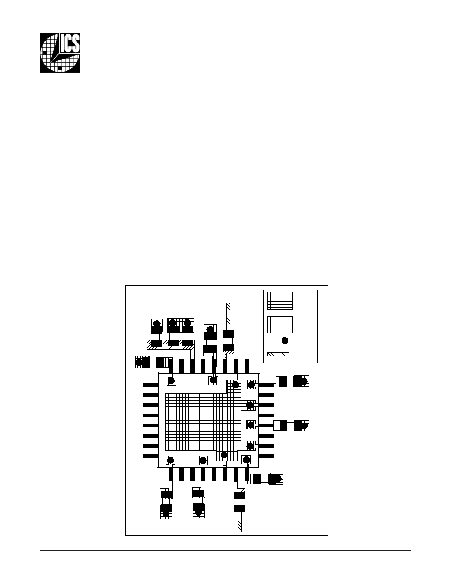
8705BY
www.icst.com/products/hiperclocks.html
REV. G JUNE 16, 2004
13
Integrated
Circuit
Systems, Inc.
ICS8705
Z
ERO
D
ELAY
, D
IFFERENTIAL
-
TO
-LVCMOS/LVTTL
C
LOCK
G
ENERATOR
Other
signals
GND
VDDA
R7
C7
50 Ohm
Trace
C11
VIA
C16
Pin 1
R2
U1
C5
50 Ohm
Trace
VDD
R1
C2
C4
C6
C1
C3
F
IGURE
4B. PCB B
OARD
L
AYOUT
F
OR
ICS8705
The following component footprints are used in this layout
example:
All the resistors and capacitors are size 0603.
P
OWER
AND
G
ROUNDING
Place the decoupling capacitors as close as possible to the power
pins. If space allows, placement of the decoupling capacitor on
the component side is preferred. This can reduce unwanted in-
ductance between the decoupling capacitor and the power pin
caused by the via.
Maximize the power and ground pad sizes and number of vias
capacitors. This can reduce the inductance between the power
and ground planes and the component power and ground pins.
The RC filter consisting of R7, C11, and C16 should be placed
as close to the V
DDA
pin as possible.
C
LOCK
T
RACES
AND
T
ERMINATION
Poor signal integrity can degrade the system performance or
cause system failure. In synchronous high-speed digital systems,
the clock signal is less tolerant to poor signal integrity than other
signals. Any ringing on the rising or falling edge or excessive ring
back can cause system failure. The shape of the trace and the
trace delay might be restricted by the available space on the board
and the component location. While routing the traces, the clock
signal traces should be routed first and should be locked prior to
routing other signal traces.
� The differential 50
output traces should have same
length.
� Avoid sharp angles on the clock trace. Sharp angle
turns cause the characteristic impedance to change on
the transmission lines.
� Keep the clock traces on the same layer. Whenever pos-
sible, avoid placing vias on the clock traces. Placement
of vias on the traces can affect the trace characteristic
impedance and hence degrade signal integrity.
� To prevent cross talk, avoid routing other signal traces in
parallel with the clock traces. If running parallel traces is
unavoidable, allow a separation of at least three trace
widths between the differential clock trace and the other
signal trace.
� Make sure no other signal traces are routed between the
clock trace pair.
� The series termination resistors should be located as
close to the driver pins as possible.

8705BY
www.icst.com/products/hiperclocks.html
REV. G JUNE 16, 2004
14
Integrated
Circuit
Systems, Inc.
ICS8705
Z
ERO
D
ELAY
, D
IFFERENTIAL
-
TO
-LVCMOS/LVTTL
C
LOCK
G
ENERATOR
R
ELIABILITY
I
NFORMATION
T
RANSISTOR
C
OUNT
The transistor count for ICS8705 is: 3126
T
ABLE
6.
JA
VS
. A
IR
F
LOW
T
ABLE
FOR
32 L
EAD
LQFP
JA
by Velocity (Linear Feet per Minute)
0
200
500
Single-Layer PCB, JEDEC Standard Test Boards
67.8�C/W
55.9�C/W
50.1�C/W
Multi-Layer PCB, JEDEC Standard Test Boards
47.9�C/W
42.1�C/W
39.4�C/W
NOTE: Most modern PCB designs use multi-layered boards. The data in the second row pertains to most designs.
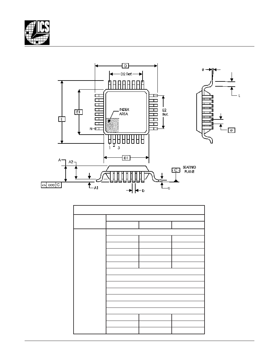
8705BY
www.icst.com/products/hiperclocks.html
REV. G JUNE 16, 2004
15
Integrated
Circuit
Systems, Inc.
ICS8705
Z
ERO
D
ELAY
, D
IFFERENTIAL
-
TO
-LVCMOS/LVTTL
C
LOCK
G
ENERATOR
P
ACKAGE
O
UTLINE
- Y S
UFFIX
FOR
32 L
EAD
LQFP
T
ABLE
7. P
ACKAGE
D
IMENSIONS
Reference Document: JEDEC Publication 95, MS-026
N
O
I
T
A
I
R
A
V
C
E
D
E
J
S
R
E
T
E
M
I
L
L
I
M
N
I
S
N
O
I
S
N
E
M
I
D
L
L
A
L
O
B
M
Y
S
A
B
B
M
U
M
I
N
I
M
L
A
N
I
M
O
N
M
U
M
I
X
A
M
N
2
3
A
-
-
-
-
0
6
.
1
1
A
5
0
.
0
-
-
5
1
.
0
2
A
5
3
.
1
0
4
.
1
5
4
.
1
b
0
3
.
0
7
3
.
0
5
4
.
0
c
9
0
.
0
-
-
0
2
.
0
D
C
I
S
A
B
0
0
.
9
1
D
C
I
S
A
B
0
0
.
7
2
D
.
f
e
R
0
6
.
5
E
C
I
S
A
B
0
0
.
9
1
E
C
I
S
A
B
0
0
.
7
2
E
.
f
e
R
0
6
.
5
e
C
I
S
A
B
0
8
.
0
L
5
4
.
0
0
6
.
0
5
7
.
0
0
�
-
-
7
�
c
c
c
-
-
-
-
0
1
.
0
8705BY
www.icst.com/products/hiperclocks.html
REV. G JUNE 16, 2004
16
Integrated
Circuit
Systems, Inc.
ICS8705
Z
ERO
D
ELAY
, D
IFFERENTIAL
-
TO
-LVCMOS/LVTTL
C
LOCK
G
ENERATOR
T
ABLE
8. O
RDERING
I
NFORMATION
While the information presented herein has been checked for both accuracy and reliability, Integrated Circuit Systems, Incorporated (ICS) assumes no responsibility for either its use or
for infringement of any patents or other rights of third parties, which would result from its use. No other circuits, patents, or licenses are implied. This product is intended for use in normal
commercial applications. Any other applications such as those requiring extended temperature range, high reliability, or other extraordinary environmental requirements are not recom-
mended without additional processing by ICS. ICS reserves the right to change any circuitry or specifications without notice. ICS does not authorize or warrant any ICS product for use
in life support devices or critical medical instruments.
r
e
b
m
u
N
r
e
d
r
O
/
t
r
a
P
g
n
i
k
r
a
M
e
g
a
k
c
a
P
t
n
u
o
C
e
r
u
t
a
r
e
p
m
e
T
Y
B
5
0
7
8
S
C
I
Y
B
5
0
7
8
S
C
I
P
F
Q
L
d
a
e
L
2
3
y
a
r
t
r
e
p
0
5
2
C
�
0
7
o
t
C
�
0
T
Y
B
5
0
7
8
S
C
I
Y
B
5
0
7
8
S
C
I
l
e
e
R
d
n
a
e
p
a
T
n
o
P
F
Q
L
d
a
e
L
2
3
0
0
0
1
C
�
0
7
o
t
C
�
0
F
L
Y
B
5
0
7
8
S
C
I
F
L
Y
B
5
0
7
8
S
C
I
P
F
Q
L
"
e
e
r
F
d
a
e
L
"
d
a
e
L
2
3
y
a
r
t
r
e
p
0
5
2
C
�
0
7
o
t
C
�
0
T
F
L
Y
B
5
0
7
8
S
C
I
F
L
Y
B
5
0
7
8
S
C
I
l
e
e
R
d
n
a
e
p
a
T
n
o
P
F
Q
L
"
e
e
r
F
d
a
e
L
"
d
a
e
L
2
3
0
0
0
1
C
�
0
7
o
t
C
�
0
The aforementioned trademark, HiPerClockSTM is a trademark of Integrated Circuit Systems, Inc. or its subsidiaries in the United States and/or other countries.
8705BY
www.icst.com/products/hiperclocks.html
REV. G JUNE 16, 2004
17
Integrated
Circuit
Systems, Inc.
ICS8705
Z
ERO
D
ELAY
, D
IFFERENTIAL
-
TO
-LVCMOS/LVTTL
C
LOCK
G
ENERATOR
T
E
E
H
S
Y
R
O
T
S
I
H
N
O
I
S
I
V
E
R
v
e
R
e
l
b
a
T
e
g
a
P
e
g
n
a
h
C
f
o
n
o
i
t
p
i
r
c
s
e
D
e
t
a
D
A
1
m
a
r
g
a
i
D
k
c
o
l
B
d
e
t
a
d
p
U
2
0
/
5
2
/
1
B
A
3
T
A
5
T
B
5
T
;
F
4
T
:
D
4
T
3
5
7
,
6
n
m
u
l
o
c
e
g
n
a
R
y
c
n
e
u
q
e
r
F
e
c
n
e
r
e
f
e
R
e
h
t
d
e
s
i
v
e
r
-
e
l
b
a
T
n
o
i
t
c
n
u
F
e
l
b
a
n
E
L
L
P
m
o
r
f
w
o
r
y
c
n
e
u
q
e
r
F
t
u
p
t
u
O
e
h
t
d
e
t
a
d
p
u
-
e
l
b
a
T
s
c
i
t
s
i
r
e
t
c
a
r
a
h
C
C
A
V
3
.
3
.
x
a
M
z
H
M
5
7
2
o
t
.
x
a
M
z
H
M
0
5
3
.
s
e
l
b
a
t
V
5
.
2
d
e
d
d
A
2
0
/
4
1
/
3
C
A
3
T
A
5
T
B
5
T
3
5
7
n
m
u
l
o
c
e
g
n
a
R
y
c
n
e
u
q
e
r
F
e
c
n
e
r
e
f
e
R
e
h
t
d
e
s
i
v
e
r
-
e
l
b
a
T
n
o
i
t
c
n
u
F
e
l
b
a
n
E
L
L
P
m
o
r
f
w
o
r
y
c
n
e
u
q
e
r
F
t
u
p
t
u
O
e
h
t
d
e
t
a
d
p
u
-
e
l
b
a
T
s
c
i
t
s
i
r
e
t
c
a
r
a
h
C
C
A
V
3
.
3
.
x
a
M
z
H
M
0
5
2
o
t
.
x
a
M
z
H
M
5
7
2
m
o
r
f
w
o
r
y
c
n
e
u
q
e
r
F
t
u
p
t
u
O
e
h
t
d
e
t
a
d
p
u
-
e
l
b
a
T
s
c
i
t
s
i
r
e
t
c
a
r
a
h
C
C
A
V
5
.
2
.
x
a
M
z
H
M
0
5
2
o
t
.
x
a
M
z
H
M
5
7
2
2
0
/
4
/
4
C
1
T
2
.
s
n
o
i
t
p
i
r
c
s
e
d
n
i
p
r
e
w
o
p
d
e
s
i
v
e
r
-
e
l
b
a
T
n
o
i
t
p
i
r
c
s
e
D
n
i
P
2
0
/
0
1
/
4
C
2
T
2
C
n
i
)
l
a
c
i
p
y
t
(
F
p
3
2
d
d
a
-
e
l
b
a
T
s
c
i
t
s
i
r
e
t
c
a
r
a
h
C
n
i
P
D
P
.
w
o
r
2
0
/
5
1
/
7
C
1
T
2
"
.
0
1
n
i
p
o
t
t
c
e
n
n
o
C
"
d
e
c
a
l
p
e
r
,
n
o
i
t
p
i
r
c
s
e
d
m
o
r
f
0
1
#
n
i
P
-
e
l
b
a
T
n
o
i
t
p
i
r
c
s
e
D
n
i
P
"
.
s
t
u
p
t
u
o
e
h
t
f
o
e
n
o
o
t
t
c
e
n
n
o
C
"
h
t
i
w
2
0
/
1
/
8
C
1
T
2
8
.
n
o
i
t
p
i
r
c
s
e
d
R
M
d
n
a
n
o
i
t
p
i
r
c
s
e
d
0
K
L
C
d
e
s
i
v
e
R
.
m
a
r
g
a
i
D
e
m
i
T
ll
a
F
/
e
s
i
R
t
u
p
t
u
O
d
e
s
i
v
e
R
2
0
/
1
2
/
8
D
D
4
T
,
A
4
T
,
1
T
B
5
T
,
A
5
T
6
,
4
,
2
7
,
5
V
r
o
f
n
o
i
t
p
i
r
c
s
e
d
d
e
s
i
v
e
R
D
D
.
y
l
p
p
u
s
e
v
i
t
i
s
o
P
m
o
r
f
y
l
p
p
u
s
e
r
o
C
d
a
e
r
o
t
s
n
o
i
t
i
d
n
o
c
t
s
e
t
t
n
e
r
e
f
f
i
d
h
t
i
w
"
c
d
o
"
o
t
w
o
r
r
e
h
t
o
n
a
d
e
d
d
a
,
s
c
i
t
s
i
r
e
t
c
a
r
a
h
C
C
A
.
s
e
u
l
a
v
d
n
a
.
t
a
m
r
o
f
d
e
t
a
d
p
U
2
0
/
2
2
/
1
1
E
1
B
5
T
&
A
5
T
2
7
&
5
.
n
o
i
t
p
i
r
c
s
e
d
R
M
d
e
s
i
v
e
r
-
e
l
b
a
t
n
o
i
t
p
i
r
c
s
e
D
n
i
P
.
1
K
L
C
n
,
1
K
L
C
r
o
f
s
t
i
m
il
t
e
s
f
f
O
e
s
a
h
P
c
i
t
a
t
S
e
h
t
d
e
g
n
a
h
C
-
s
e
l
b
a
t
C
A
3
0
/
2
2
/
1
F
B
5
T
&
A
5
T
7
&
5
.
"
2
*
x
Q
,
z
H
M
6
6
=
F
E
R
f
"
h
t
i
w
t
e
s
f
f
O
e
s
a
h
P
c
i
t
a
t
S
d
e
d
d
a
-
s
e
l
b
a
t
C
A
4
E
T
O
N
d
a
e
r
o
t
r
e
t
e
m
a
r
a
p
O
P
S
n
i
o
p
y
t
d
e
t
c
e
r
r
o
c
-
e
l
b
a
t
C
A
V
3
.
3
.
7
E
T
O
N
m
o
r
f
"
.
.
.
L
T
T
V
L
/
S
O
M
C
V
L
-
o
t
-
l
a
i
t
n
e
r
e
f
f
i
D
.
.
.
"
d
a
e
r
o
t
e
l
t
i
t
d
e
s
i
v
e
r
t
e
e
h
s
a
t
a
d
t
u
o
h
g
u
o
r
h
T
3
0
/
3
1
/
2
G
B
5
T
7
9
.
5
e
t
o
N
d
n
a
,
c
e
p
s
r
e
t
t
i
J
e
s
a
h
P
d
e
d
d
a
-
e
l
b
a
T
s
c
i
t
s
i
r
e
t
c
a
r
a
h
C
C
A
V
5
.
2
.
m
a
r
g
a
i
D
O
P
S
&
r
e
t
t
i
J
e
s
a
h
P
h
t
i
w
m
a
r
g
a
i
D
t
e
s
f
f
O
e
s
a
h
P
c
i
t
a
t
S
d
e
c
a
l
p
e
R
3
0
/
4
1
/
3
G
2
T
2
1
1
C
d
e
g
n
a
h
c
-
e
l
b
a
T
s
c
i
t
s
i
r
e
t
c
a
r
a
h
C
n
i
P
N
I
.
l
a
c
i
p
y
t
F
p
4
o
t
.
x
a
m
F
p
4
m
o
r
f
.
n
o
i
t
c
e
s
e
c
a
f
r
e
t
n
I
t
u
p
n
I
k
c
o
l
C
l
a
i
t
n
e
r
e
f
f
i
D
d
e
d
d
A
3
0
/
5
1
/
5
G
3
1
&
2
1
e
n
il
e
d
i
u
G
t
u
o
y
a
L
d
e
d
d
A
3
0
/
6
/
6
G
6
T
4
1
r
e
b
m
u
n
t
r
a
p
"
e
e
r
F
-
d
a
e
L
"
d
e
d
d
a
-
e
l
b
a
T
n
o
i
t
a
m
r
o
f
n
I
g
n
i
r
e
d
r
O
4
0
/
6
1
/
6