 | –≠–ª–µ–∫—Ç—Ä–æ–Ω–Ω—ã–π –∫–æ–º–ø–æ–Ω–µ–Ω—Ç: ICS8737 | –°–∫–∞—á–∞—Ç—å:  PDF PDF  ZIP ZIP |
8737AG-11
www.icst.com/products/hiperclocks.html
REV. A JUNE 3, 2002
1
Integrated
Circuit
Systems, Inc.
ICS8737-11
L
OW
S
KEW
,
∏
1/
∏
2
D
IFFERENTIAL
-
TO
- 3.3V LVPECL C
LOCK
G
ENERATOR
G
ENERAL
D
ESCRIPTION
The ICS8737-11 is a low skew, high performance
Differential-to-3.3V LVPECL Clock Generator/
Divider and a member of the HiPerClockSTM
family of High Performance Clock Solutions from
ICS. The ICS8737-11 has two selectable clock
inputs. The CLK, nCLK pair can accept most standard differ-
ential input levels. The PCLK, nPCLK pair can accept
LVPECL, CML, or SSTL input levels.The clock enable is
internally synchronized to eliminate runt pulses on the
outputs during asynchronous assertion/deassertion of the
clock enable pin.
Guaranteed output and part-to-part skew characteristics
make the ICS8737-11 ideal for clock distribution applications
demanding well defined performance and repeatability.
F
EATURES
∑
2 divide by 1 differential 3.3V LVPECL outputs;
2 divide by 2 differential 3.3V LVPECL outputs
∑
Selectable differential CLK, nCLK or LVPECL clock inputs
∑
CLK, nCLK pair can accept the following differential
input levels: LVDS, LVPECL, LVHSTL, SSTL, HCSL
∑
PCLK, nPCLK supports the following input types:
LVPECL, CML, SSTL
∑
Maximum output frequency: 650MHz
∑
Translates any single ended input signal (LVCMOS, LVTTL,
GTL) to LVPECL levels with resistor bias on nCLK input
∑
Output skew: 60ps (maximum)
∑
Part-to-part skew: 200ps (maximum)
∑
Bank skew: Bank A - 20ps (maximum),
Bank B - 35ps (maximum)
∑
Propagation delay: 1.7ns (maximum)
∑
3.3V operating supply
∑
0∞C to 70∞C ambient operating temperature
∑
Industrial temperature information available upon request
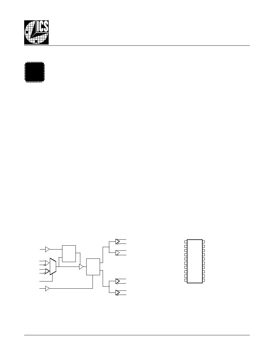
B
LOCK
D
IAGRAM
P
IN
A
SSIGNMENT
ICS8737-11
20-Lead TSSOP
6.50mm x 4.40mm x 0.92 package body
G Package
Top View
V
EE
CLK_EN
CLK_SEL
CLK
nCLK
PCLK
nPCLK
nc
MR
V
CC
1
2
3
4
5
6
7
8
9
10
20
19
18
17
16
15
14
13
12
11
QA0
nQA0
V
CC
QA1
nQA1
QB0
nQB0
V
CC
QB1
nQB1
HiPerClockSTM
,&6
QA0
nQA0
QA1
nQA1
˜
1
˜
2
D
Q
LE
CLK_EN
CLK
nCLK
PCLK
nPCLK
MR
QB0
nQB0
QB1
nQB1
CLK_SEL
0
1
8737AG-11
www.icst.com/products/hiperclocks.html
REV. A JUNE 3, 2002
2
Integrated
Circuit
Systems, Inc.
ICS8737-11
L
OW
S
KEW
,
∏
1/
∏
2
D
IFFERENTIAL
-
TO
- 3.3V LVPECL C
LOCK
G
ENERATOR
T
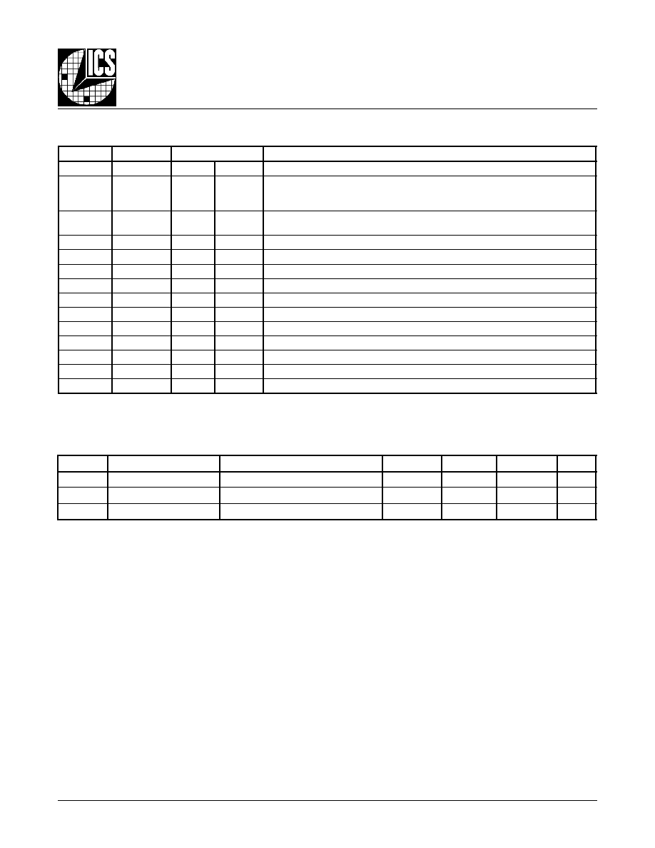
ABLE
2. P
IN
C
HARACTERISTICS
T
ABLE
1. P
IN
D
ESCRIPTIONS
l
o
b
m
y
S
r
e
t
e
m
a
r
a
P
s
n
o
i
t
i
d
n
o
C
t
s
e
T
m
u
m
i
n
i
M
l
a
c
i
p
y
T
m
u
m
i
x
a
M
s
t
i
n
U
C
N
I
e
c
n
a
t
i
c
a
p
a
C
t
u
p
n
I
4
F
p
R
P
U
L
L
U
P
r
o
t
s
i
s
e
R
p
u
ll
u
P
t
u
p
n
I
1
5
K
R
N
W
O
D
L
L
U
P
r
o
t
s
i
s
e
R
n
w
o
d
ll
u
P
t
u
p
n
I
1
5
K
r
e
b
m
u
N
e
m
a
N
e
p
y
T
n
o
i
t
p
i
r
c
s
e
D
1
V
E
E
r
e
w
o
P
.
n
i
p
y
l
p
p
u
s
e
v
i
t
a
g
e
N
2
N
E
_
K
L
C
r
e
w
o
P
p
u
ll
u
P
.
t
u
p
n
i
k
c
o
l
c
w
o
ll
o
f
s
t
u
p
t
u
o
k
c
o
l
c
,
H
G
I
H
n
e
h
W
.
e
l
b
a
n
e
k
c
o
l
c
g
n
i
z
i
n
o
r
h
c
n
y
S
.
h
g
i
h
d
e
c
r
o
f
e
r
a
s
t
u
p
t
u
o
Q
n
,
w
o
l
d
e
c
r
o
f
e
r
a
s
t
u
p
t
u
o
Q
,
W
O
L
n
e
h
W
.
s
l
e
v
e
l
e
c
a
f
r
e
t
n
i
S
O
M
C
V
L
/
L
T
T
V
L
3
L
E
S
_
K
L
C
t
u
p
n
I
n
w
o
d
ll
u
P
.
s
t
u
p
n
i
K
L
C
P
n
,
K
L
C
P
s
t
c
e
l
e
s
,
H
G
I
H
n
e
h
W
.
t
u
p
n
i
t
c
e
l
e
S
k
c
o
l
C
.
s
l
e
v
e
l
e
c
a
f
r
e
t
n
i
S
O
M
C
V
L
/
L
T
T
V
L
.
s
t
u
p
n
i
K
L
C
n
,
K
L
C
s
t
c
e
l
e
s
,
W
O
L
n
e
h
W
4
K
L
C
t
u
p
n
I
n
w
o
d
ll
u
P
.
t
u
p
n
i
k
c
o
l
c
l
a
i
t
n
e
r
e
f
f
i
d
g
n
i
t
r
e
v
n
i
-
n
o
N
5
K
L
C
n
t
u
p
n
I
p
u
ll
u
P
.
t
u
p
n
i
k
c
o
l
c
l
a
i
t
n
e
r
e
f
f
i
d
g
n
i
t
r
e
v
n
I
6
K
L
C
P
t
u
p
n
I
n
w
o
d
ll
u
P
.
t
u
p
n
i
k
c
o
l
c
L
C
E
P
V
L
l
a
i
t
n
e
r
e
f
f
i
d
g
n
i
t
r
e
v
n
i
-
n
o
N
7
K
L
C
P
n
t
u
p
n
I
p
u
ll
u
P
.
t
u
p
n
i
k
c
o
l
c
L
C
E
P
V
L
l
a
i
t
n
e
r
e
f
f
i
d
g
n
i
t
r
e
v
n
I
8
c
n
d
e
s
u
n
U
.
t
c
e
n
n
o
c
o
N
9
R
M
t
u
p
n
I
n
w
o
d
ll
u
P
.
s
l
e
v
e
l
e
c
a
f
r
e
t
n
i
S
O
M
C
V
L
/
L
T
T
V
L
.
r
e
d
i
v
i
d
t
u
p
t
u
o
e
h
t
s
t
e
s
e
R
.
t
e
s
e
r
r
e
t
s
a
M
8
1
,
3
1
,
0
1
V
C
C
r
e
w
o
P
.
s
n
i
p
y
l
p
p
u
s
e
v
i
t
i
s
o
P
2
1
,
1
1
1
B
Q
,
1
B
Q
n
t
u
p
t
u
O
.
s
l
e
v
e
l
e
c
a
f
r
e
t
n
i
L
C
E
P
V
L
.
r
i
a
p
t
u
p
t
u
o
l
a
i
t
n
e
r
e
f
f
i
D
5
1
,
4
1
0
B
Q
,
0
B
Q
n
t
u
p
t
u
O
.
s
l
e
v
e
l
e
c
a
f
r
e
t
n
i
L
C
E
P
V
L
.
r
i
a
p
t
u
p
t
u
o
l
a
i
t
n
e
r
e
f
f
i
D
7
1
,
6
1
1
A
Q
,
1
A
Q
n
t
u
p
t
u
O
.
s
l
e
v
e
l
e
c
a
f
r
e
t
n
i
L
C
E
P
V
L
.
r
i
a
p
t
u
p
t
u
o
l
a
i
t
n
e
r
e
f
f
i
D
0
2
,
9
1
0
A
Q
,
0
A
Q
n
t
u
p
t
u
O
.
s
l
e
v
e
l
e
c
a
f
r
e
t
n
i
L
C
E
P
V
L
.
r
i
a
p
t
u
p
t
u
o
l
a
i
t
n
e
r
e
f
f
i
D
:
E
T
O
N
p
u
ll
u
P
d
n
a
n
w
o
d
ll
u
P
.
s
e
u
l
a
v
l
a
c
i
p
y
t
r
o
f
,
s
c
i
t
s
i
r
e
t
c
a
r
a
h
C
n
i
P
,
2
e
l
b
a
T
e
e
S
.
s
r
o
t
s
i
s
e
r
t
u
p
n
i
l
a
n
r
e
t
n
i
o
t
r
e
f
e
r
8737AG-11
www.icst.com/products/hiperclocks.html
REV. A JUNE 3, 2002
3
Integrated
Circuit
Systems, Inc.
ICS8737-11
L
OW
S
KEW
,
∏
1/
∏
2
D
IFFERENTIAL
-
TO
- 3.3V LVPECL C
LOCK
G
ENERATOR
T
ABLE
3A. C
ONTROL
I
NPUT
F
UNCTION
T
ABLE
T
ABLE
3B. C
LOCK
I
NPUT
F
UNCTION
T
ABLE
s
t
u
p
n
I
s
t
u
p
t
u
O
R
M
N
E
_
K
L
C
L
E
S
_
K
L
C
e
c
r
u
o
S
d
e
t
c
e
l
e
S
1
A
Q
,
0
A
Q
1
A
Q
n
,
0
A
Q
n
1
B
Q
,
0
B
Q
1
B
Q
n
,
0
B
Q
n
1
X
X
X
W
O
L
H
G
I
H
W
O
L
H
G
I
H
0
0
0
K
L
C
n
,
K
L
C
W
O
L
;
d
e
l
b
a
s
i
D
H
G
I
H
;
d
e
l
b
a
s
i
D
W
O
L
;
d
e
l
b
a
s
i
D
H
G
I
H
;
d
e
l
b
a
s
i
D
0
0
1
K
L
C
P
n
,
K
L
C
P
W
O
L
;
d
e
l
b
a
s
i
D
H
G
I
H
;
d
e
l
b
a
s
i
D
W
O
L
;
d
e
l
b
a
s
i
D
H
G
I
H
;
d
e
l
b
a
s
i
D
0
1
0
K
L
C
n
,
K
L
C
d
e
l
b
a
n
E
d
e
l
b
a
n
E
d
e
l
b
a
n
E
d
e
l
b
a
n
E
0
1
1
K
L
C
P
n
,
K
L
C
P
d
e
l
b
a
n
E
d
e
l
b
a
n
E
d
e
l
b
a
n
E
d
e
l
b
a
n
E
e
g
d
e
k
c
o
l
c
t
u
p
n
i
g
n
il
l
a
f
d
n
a
g
n
i
s
i
r
a
g
n
i
w
o
ll
o
f
d
e
l
b
a
n
e
r
o
d
e
l
b
a
s
i
d
e
r
a
s
t
u
p
t
u
o
k
c
o
l
c
e
h
t
,
s
e
h
c
t
i
w
s
N
E
_
K
L
C
r
e
t
f
A
.
1
e
r
u
g
i
F
f
i
n
w
o
h
s
s
a
d
e
b
i
r
c
s
e
d
s
a
s
t
u
p
n
i
K
L
C
P
n
,
K
L
C
P
d
n
a
K
L
C
n
,
K
L
C
e
h
t
f
o
n
o
i
t
c
n
u
f
a
e
r
a
s
t
u
p
t
u
o
e
h
t
f
o
e
t
a
t
s
e
h
t
,
e
d
o
m
e
v
i
t
c
a
e
h
t
n
I
.
B
3
e
l
b
a
T
n
i
s
t
u
p
n
I
s
t
u
p
t
u
O
e
d
o
M
t
u
p
t
u
O
o
t
t
u
p
n
I
y
t
i
r
a
l
o
P
K
L
C
P
r
o
K
L
C
K
L
C
P
n
r
o
K
L
C
n
x
A
Q
x
A
Q
n
x
B
Q
x
B
Q
n
0
0
W
O
L
H
G
I
H
W
O
L
H
G
I
H
l
a
i
t
n
e
r
e
f
f
i
D
o
t
l
a
i
t
n
e
r
e
f
f
i
D
g
n
i
t
r
e
v
n
I
n
o
N
1
1
H
G
I
H
W
O
L
H
G
I
H
W
O
L
l
a
i
t
n
e
r
e
f
f
i
D
o
t
l
a
i
t
n
e
r
e
f
f
i
D
g
n
i
t
r
e
v
n
I
n
o
N
0
1
E
T
O
N
;
d
e
s
a
i
B
W
O
L
H
G
I
H
W
O
L
H
G
I
H
l
a
i
t
n
e
r
e
f
f
i
D
o
t
d
e
d
n
E
e
l
g
n
i
S
g
n
i
t
r
e
v
n
I
n
o
N
1
1
E
T
O
N
;
d
e
s
a
i
B
H
G
I
H
W
O
L
H
G
I
H
W
O
L
l
a
i
t
n
e
r
e
f
f
i
D
o
t
d
e
d
n
E
e
l
g
n
i
S
g
n
i
t
r
e
v
n
I
n
o
N
1
E
T
O
N
;
d
e
s
a
i
B
0
H
G
I
H
W
O
L
H
G
I
H
W
O
L
l
a
i
t
n
e
r
e
f
f
i
D
o
t
d
e
d
n
E
e
l
g
n
i
S
g
n
i
t
r
e
v
n
I
1
E
T
O
N
;
d
e
s
a
i
B
1
W
O
L
H
G
I
H
W
O
L
H
G
I
H
l
a
i
t
n
e
r
e
f
f
i
D
o
t
d
e
d
n
E
e
l
g
n
i
S
g
n
i
t
r
e
v
n
I
.
"
s
l
e
v
e
L
d
e
d
n
E
e
l
g
n
i
S
t
p
e
c
c
A
o
t
t
u
p
n
I
l
a
i
t
n
e
r
e
f
f
i
D
e
h
t
g
n
i
r
i
W
"
,
n
o
i
t
c
e
s
n
o
i
t
a
m
r
o
f
n
I
n
o
i
t
a
c
il
p
p
A
e
h
t
o
t
r
e
f
e
r
e
s
a
e
l
P
:
1
E
T
O
N
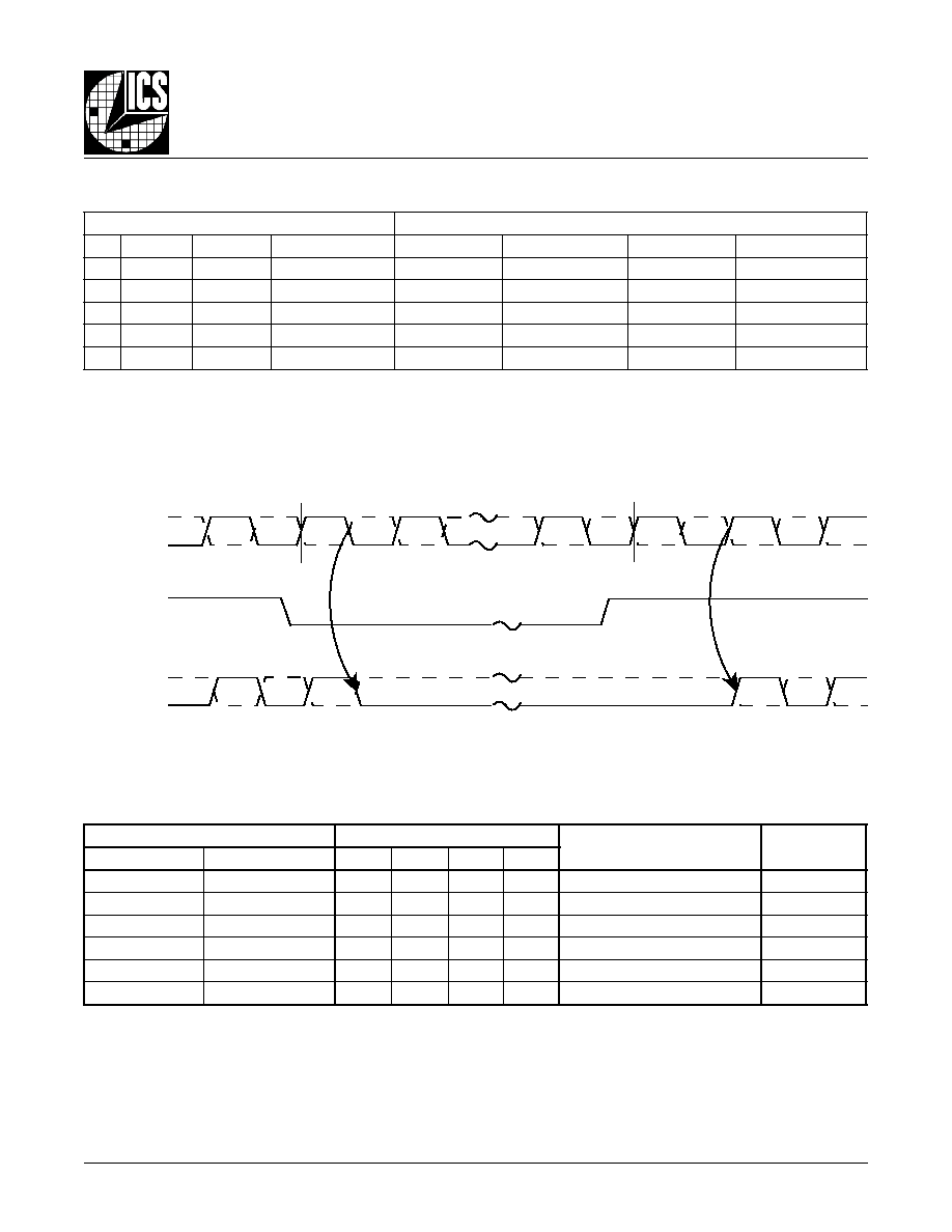
Enabled
Disabled
F
IGURE
1 - CLK_EN T
IMING
D
IAGRAM
nCLK, nPCLK
CLK, PCLK
CLK_EN
nQA0, nQA1,
nQB0, nQB1
QA0, QA1,
QB0, QB1

8737AG-11
www.icst.com/products/hiperclocks.html
REV. A JUNE 3, 2002
4
Integrated
Circuit
Systems, Inc.
ICS8737-11
L
OW
S
KEW
,
∏
1/
∏
2
D
IFFERENTIAL
-
TO
- 3.3V LVPECL C
LOCK
G
ENERATOR
A
BSOLUTE
M
AXIMUM
R
ATINGS
Supply Voltage, V
CC
4.6V
Inputs, V
I
-0.5V to V
CC
+ 0.5V
Outputs, V
O
-0.5V to V
CC
+ 0.5V
Package Thermal Impedance,
JA
73.2∞C/W (0 lfpm)
Storage Temperature, T
STG
-65∞C to 150∞C
Stresses beyond those listed under Absolute Maximum Ratings may cause permanent damage to the device. These ratings
are stress specifications only. Functional operation of product at these conditions or any conditions beyond those listed in the
DC Characteristics or AC Characteristics is not implied. Exposure to absolute maximum rating conditions for extended peri-
ods may affect product reliability.
T
ABLE
4A. P
OWER
S
UPPLY
DC C
HARACTERISTICS
,
V
CC
= 3.3V±5%, T
A
= 0∞C
TO
70∞C
T
ABLE
4B. LVCMOS / LVTTL DC C
HARACTERISTICS
,
V
CC
= 3.3V±5%, T
A
= 0∞C
TO
70∞C
T
ABLE
4C. D
IFFERENTIAL
DC C
HARACTERISTICS
,
V
CC
= 3.3V±5%, T
A
= 0∞C
TO
70∞C
l
o
b
m
y
S
r
e
t
e
m
a
r
a
P
s
n
o
i
t
i
d
n
o
C
t
s
e
T
m
u
m
i
n
i
M
l
a
c
i
p
y
T
m
u
m
i
x
a
M
s
t
i
n
U
V
C
C
e
g
a
t
l
o
V
y
l
p
p
u
S
e
v
i
t
i
s
o
P
5
3
1
.
3
3
.
3
5
6
4
.
3
V
I
E
E
t
n
e
r
r
u
C
y
l
p
p
u
S
r
e
w
o
P
0
5
A
m
l
o
b
m
y
S
r
e
t
e
m
a
r
a
P
s
n
o
i
t
i
d
n
o
C
t
s
e
T
m
u
m
i
n
i
M
l
a
c
i
p
y
T
m
u
m
i
x
a
M
s
t
i
n
U
V
H
I
R
M
,
L
E
S
_
K
L
C
,
N
E
_
K
L
C
2
5
6
7
.
3
V
V
L
I
R
M
,
L
E
S
_
K
L
C
,
N
E
_
K
L
C
3
.
0
-
8
.
0
V
I
H
I
t
n
e
r
r
u
C
h
g
i
H
t
u
p
n
I
N
E
_
K
L
C
V
N
I
V
=
C
C
V
5
6
4
.
3
=
5
A
µ
R
M
,
L
E
S
_
K
L
C
V
N
I
V
=
C
C
V
5
6
4
.
3
=
0
5
1
A
µ
I
L
I
t
n
e
r
r
u
C
w
o
L
t
u
p
n
I
N
E
_
K
L
C
V
N
I
V
,
V
0
=
C
C
V
5
6
4
.
3
=
0
5
1
-
A
µ
R
M
,
L
E
S
_
K
L
C
V
N
I
V
,
V
0
=
C
C
V
5
6
4
.
3
=
5
-
A
µ
l
o
b
m
y
S
r
e
t
e
m
a
r
a
P
s
n
o
i
t
i
d
n
o
C
t
s
e
T
m
u
m
i
n
i
M
l
a
c
i
p
y
T
m
u
m
i
x
a
M
s
t
i
n
U
I
H
I
t
n
e
r
r
u
C
h
g
i
H
t
u
p
n
I
K
L
C
n
V
N
I
V
=
C
C
V
5
6
4
.
3
=
5
A
µ
K
L
C
V
N
I
V
=
C
C
V
5
6
4
.
3
=
0
5
1
A
µ
I
L
I
t
n
e
r
r
u
C
w
o
L
t
u
p
n
I
K
L
C
n
V
N
I
V
,
V
0
=
C
C
V
5
6
4
.
3
=
0
5
1
-
A
µ
K
L
C
V
N
I
V
,
V
0
=
C
C
V
5
6
4
.
3
=
5
-
A
µ
V
P
P
e
g
a
t
l
o
V
t
u
p
n
I
k
a
e
P
-
o
t
-
k
a
e
P
5
1
.
0
3
.
1
V
V
R
M
C
;
e
g
a
t
l
o
V
t
u
p
n
I
e
d
o
M
n
o
m
m
o
C
2
,
1
E
T
O
N
V
E
E
5
.
0
+
V
C
C
5
8
.
0
-
V
s
n
o
i
t
a
c
il
p
p
a
d
e
d
n
e
e
l
g
n
i
s
r
o
F
:
1
E
T
O
N
,
V
s
i
K
L
C
n
,
K
L
C
r
o
f
e
g
a
t
l
o
v
t
u
p
n
i
m
u
m
i
x
a
m
e
h
t
C
C
.
V
3
.
0
+
s
i
e
g
a
t
l
o
v
e
d
o
m
n
o
m
m
o
C
:
2
E
T
O
N
V
s
a
d
e
n
i
f
e
d
H
I
.
8737AG-11
www.icst.com/products/hiperclocks.html
REV. A JUNE 3, 2002
5
Integrated
Circuit
Systems, Inc.
ICS8737-11
L
OW
S
KEW
,
∏
1/
∏
2
D
IFFERENTIAL
-
TO
- 3.3V LVPECL C
LOCK
G
ENERATOR
T
ABLE
5. AC C
HARACTERISTICS
,
V
CC
= 3.3V±5%, T
A
= 0∞C
TO
70∞C
T
ABLE
4D. LVPECL DC C
HARACTERISTICS
,
V
CC
= 3.3V±5%, T
A
= 0∞C
TO
70∞C
l
o
b
m
y
S
r
e
t
e
m
a
r
a
P
s
n
o
i
t
i
d
n
o
C
t
s
e
T
m
u
m
i
n
i
M
l
a
c
i
p
y
T
m
u
m
i
x
a
M
s
t
i
n
U
f
X
A
M
y
c
n
e
u
q
e
r
F
t
u
p
t
u
O
0
5
6
z
H
M
t
D
P
1
E
T
O
N
;
y
a
l
e
D
n
o
i
t
a
g
a
p
o
r
P
K
L
C
n
,
K
L
C
z
H
M
0
5
6
3
.
1
7
.
1
s
n
K
L
C
P
n
,
K
L
C
P
2
.
1
6
.
1
s
n
t
)
o
(
k
s
4
,
2
E
T
O
N
;
w
e
k
S
t
u
p
t
u
O
0
6
s
p
t
)
b
(
k
s
4
E
T
O
N
;
w
e
k
S
k
n
a
B
A
k
n
a
B
0
2
s
p
B
k
n
a
B
5
3
s
p
t
)
p
p
(
k
s
4
,
3
E
T
O
N
;
w
e
k
S
t
r
a
P
-
o
t
-
t
r
a
P
0
0
2
s
p
t
R
e
m
i
T
e
s
i
R
t
u
p
t
u
O
z
H
M
0
5
@
%
0
8
o
t
%
0
2
0
0
3
0
0
7
s
p
t
F
e
m
i
T
ll
a
F
t
u
p
t
u
O
z
H
M
0
5
@
%
0
8
o
t
%
0
2
0
0
3
0
0
7
s
p
c
d
o
e
l
c
y
C
y
t
u
D
t
u
p
t
u
O
8
4
0
5
2
5
%
.
e
s
i
w
r
e
h
t
o
d
e
t
o
n
s
s
e
l
n
u
z
H
M
0
0
5
t
a
d
e
r
u
s
a
e
m
s
r
e
t
e
m
a
r
a
p
ll
A
.
r
e
t
t
ij
d
d
a
t
o
n
s
e
o
d
t
r
a
p
e
h
T
.
t
u
p
t
u
o
e
h
t
n
o
r
e
t
t
ij
e
h
t
l
a
u
q
e
ll
i
w
t
u
p
n
i
e
h
t
n
o
r
e
t
t
ij
e
l
c
y
c
-
o
t
-
e
l
c
y
c
e
h
T
.
t
n
i
o
p
g
n
i
s
s
o
r
c
t
u
p
t
u
o
l
a
i
t
n
e
r
e
f
f
i
d
e
h
t
o
t
t
n
i
o
p
g
n
i
s
s
o
r
c
t
u
p
n
i
l
a
i
t
n
e
r
e
f
f
i
d
e
h
t
m
o
r
f
d
e
r
u
s
a
e
M
:
1
E
T
O
N
.
s
n
o
i
t
i
d
n
o
c
d
a
o
l
l
a
u
q
e
h
t
i
w
d
n
a
e
g
a
t
l
o
v
y
l
p
p
u
s
e
m
a
s
e
h
t
t
a
s
t
u
p
t
u
o
n
e
e
w
t
e
b
w
e
k
s
s
a
d
e
n
i
f
e
D
:
2
E
T
O
N
.
s
t
n
i
o
p
s
s
o
r
c
l
a
i
t
n
e
r
e
f
f
i
d
t
u
p
t
u
o
e
h
t
t
a
d
e
r
u
s
a
e
M
s
e
g
a
t
l
o
v
y
l
p
p
u
s
e
m
a
s
e
h
t
t
a
g
n
i
t
a
r
e
p
o
s
e
c
i
v
e
d
t
n
e
r
e
f
f
i
d
n
o
s
t
u
p
t
u
o
n
e
e
w
t
e
b
w
e
k
s
s
a
d
e
n
i
f
e
D
:
3
E
T
O
N
d
e
r
u
s
a
e
m
e
r
a
s
t
u
p
t
u
o
e
h
t
,
e
c
i
v
e
d
h
c
a
e
n
o
s
t
u
p
n
i
f
o
e
p
y
t
e
m
a
s
e
h
t
g
n
i
s
U
.
s
n
o
i
t
i
d
n
o
c
d
a
o
l
l
a
u
q
e
h
t
i
w
d
n
a
.
s
t
n
i
o
p
s
s
o
r
c
l
a
i
t
n
e
r
e
f
f
i
d
e
h
t
t
a
.
5
6
d
r
a
d
n
a
t
S
C
E
D
E
J
h
t
i
w
e
c
n
a
d
r
o
c
c
a
n
i
d
e
n
i
f
e
d
s
i
r
e
t
e
m
a
r
a
p
s
i
h
T
:
4
E
T
O
N
l
o
b
m
y
S
r
e
t
e
m
a
r
a
P
s
n
o
i
t
i
d
n
o
C
t
s
e
T
m
u
m
i
n
i
M
l
a
c
i
p
y
T
m
u
m
i
x
a
M
s
t
i
n
U
I
H
I
t
n
e
r
r
u
C
h
g
i
H
t
u
p
n
I
V
N
I
V
=
C
C
V
5
6
4
.
3
=
0
5
1
A
µ
V
N
I
V
=
C
C
V
5
6
4
.
3
=
5
A
µ
I
L
I
t
n
e
r
r
u
C
w
o
L
t
u
p
n
I
V
N
I
V
,
V
0
=
C
C
V
5
6
4
.
3
=
5
-
A
µ
V
N
I
V
,
V
0
=
C
C
V
5
6
4
.
3
=
0
5
1
-
A
µ
V
P
P
e
g
a
t
l
o
V
t
u
p
n
I
k
a
e
P
-
o
t
-
k
a
e
P
3
.
0
1
V
V
R
M
C
2
,
1
E
T
O
N
;
e
g
a
t
l
o
V
t
u
p
n
I
e
d
o
M
n
o
m
m
o
C
V
E
E
5
.
1
+
V
C
C
V
V
H
O
3
E
T
O
N
;
e
g
a
t
l
o
V
h
g
i
H
t
u
p
t
u
O
V
C
C
4
.
1
-
V
C
C
0
.
1
-
V
V
L
O
3
E
T
O
N
;
e
g
a
t
l
o
V
w
o
L
t
u
p
t
u
O
V
C
C
0
.
2
-
V
C
C
7
.
1
-
V
V
G
N
I
W
S
g
n
i
w
S
e
g
a
t
l
o
V
t
u
p
t
u
O
k
a
e
P
-
o
t
-
k
a
e
P
5
6
.
0
9
.
0
V
V
s
a
d
e
n
i
f
e
d
s
i
e
g
a
t
l
o
v
e
d
o
m
n
o
m
m
o
C
:
1
E
T
O
N
H
I
.
V
s
i
K
L
C
P
n
,
K
L
C
P
r
o
f
e
g
a
t
l
o
v
t
u
p
n
i
m
u
m
i
x
a
m
e
h
t
,
s
n
o
i
t
a
c
il
p
p
a
d
e
d
n
e
e
l
g
n
i
s
r
o
F
:
2
E
T
O
N
C
C
.
V
3
.
0
+
0
5
h
t
i
w
d
e
t
a
n
i
m
r
e
t
s
t
u
p
t
u
O
:
3
E
T
O
N
V
o
t
C
C
.
V
2
-

8737AG-11
www.icst.com/products/hiperclocks.html
REV. A JUNE 3, 2002
6
Integrated
Circuit
Systems, Inc.
ICS8737-11
L
OW
S
KEW
,
∏
1/
∏
2
D
IFFERENTIAL
-
TO
- 3.3V LVPECL C
LOCK
G
ENERATOR
tsk(o)
nQx
Qx
nQy
Qy
P
ARAMETER
M
EASUREMENT
I
NFORMATION
O
UTPUT
L
OAD
T
EST
C
IRCUIT
SCOPE
Qx
nQx
LVPECL
V
CC
= 2.0V
V
CC
O
UTPUT
S
KEW
D
IFFERENTIAL
I
NPUT
L
EVEL
V
CMR
Cross Points
V
PP
nCLK, nPCLK
CLK, PCLK
V
EE
V
CC
V
EE
= -1.3V
±
0.135V
8737AG-11
www.icst.com/products/hiperclocks.html
REV. A JUNE 3, 2002
7
Integrated
Circuit
Systems, Inc.
ICS8737-11
L
OW
S
KEW
,
∏
1/
∏
2
D
IFFERENTIAL
-
TO
- 3.3V LVPECL C
LOCK
G
ENERATOR
I
NPUT
AND
O
UTPUT
R
ISE
AND
F
ALL
T
IME
Clock Inputs
and Outputs
20%
80%
80%
20%
t
R
t
F
V
S W I N G
odc & t
P
ERIOD
Pulse Width
t
PERIOD
t
PW
t
PERIOD
odc =
nQA0, nQA1, nQB0, nQB1
QA0, QA1, QB0, QB1
P
ART
-
TO
-P
ART
S
KEW
nQx
Qx
nQy
Qy
PART 1
PART 2
tsk(pp)
P
ROPAGATION
D
ELAY
t
PD
CLK, PCLK
nQA0, nQA1, nQB0, nQB1
QA0, QA1, QB0, QB1
nCLK, nPCLK
8737AG-11
www.icst.com/products/hiperclocks.html
REV. A JUNE 3, 2002
8
Integrated
Circuit
Systems, Inc.
ICS8737-11
L
OW
S
KEW
,
∏
1/
∏
2
D
IFFERENTIAL
-
TO
- 3.3V LVPECL C
LOCK
G
ENERATOR
A
PPLICATION
I
NFORMATION
W
IRING
THE
D
IFFERENTIAL
I
NPUT
TO
A
CCEPT
S
INGLE
E
NDED
L
EVELS
Figure 2 shows how the differential input can be wired to accept single ended levels. The reference voltage V_REF ~ V
CC
/2 is
generated by the bias resistors R1, R2 and C1. This bias circuit should be located as close as possible to the input pin. The ratio of
R1 and R2 might need to be adjusted to position the V_REF in the center of the input voltage swing. For example, if the input clock
swing is only 2.5V and V
CC
= 3.3V, V_REF should be 1.25V and R2/R1 = 0.609.
F
IGURE
2 - S
INGLE
E
NDED
S
IGNAL
D
RIVING
D
IFFERENTIAL
I
NPUT
R2
1K
V
CC
CLK_IN
+
-
R1
1K
C1
0.1uF
V_REF
The clock layout topology shown below is a typical termina-
tion for LVPECL outputs. The two different layouts mentioned
are recommended only as guidelines.
FOUT and nFOUT are low impedance follower outputs that gen-
erate ECL/LVPECL compatible outputs. Therefore, terminating
resistors (DC current path to ground) or current sources must
be used for functionality. These outputs are designed to drive
3.3V
F
OUT
F
IN
5
2 Z
o
Z
o
5
2
Z
o
3
2
Z
o
3
2
Z
o
= 50
Z
o
= 50
RTT =
1
(V
OH
+ V
OL
/ V
CC
≠2) ≠2
Z
o
Z
o
= 50
Z
o
= 50
50
50
RTT
V
CC
- 2V
F
IN
F
OUT
50
transmission lines. Matched impedance techniques should
be used to maximize operating frequency and minimize signal
distortion.
Figures 3A and 3B show two different layouts which
are recommended only as guidelines. Other suitable clock lay-
outs may exist and it would be recommended that the board
designers simulate to guarantee compatibility across all printed
circuit and clock component process variations.
T
ERMINATION
FOR
LVPECL O
UTPUTS
F
IGURE
3B - LVPECL O
UTPUT
T
ERMINATION
F
IGURE
3A - LVPECL O
UTPUT
T
ERMINATION

8737AG-11
www.icst.com/products/hiperclocks.html
REV. A JUNE 3, 2002
9
Integrated
Circuit
Systems, Inc.
ICS8737-11
L
OW
S
KEW
,
∏
1/
∏
2
D
IFFERENTIAL
-
TO
- 3.3V LVPECL C
LOCK
G
ENERATOR
P
OWER
C
ONSIDERATIONS
This section provides information on power dissipation and junction temperature for the ICS8737-11.
Equations and example calculations are also provided.
1. Power Dissipation.
The total power dissipation for the ICS8737-11 is the sum of the core power plus the power dissipated in the load(s).
The following is the power dissipation for V
CC
= 3.3V + 5% = 3.465V, which gives worst case results.
NOTE: Please refer to Section 3 for details on calculating power dissipated in the load.
∑
Power (core)
MAX
= V
CC_MAX
* I
CC_MAX
= 3.465V * 50mA = 173.25mW
∑
Power (outputs)
MAX
= 30.2mW/Loaded Output pair
If all outputs are loaded, the total power is 4 * 30.2mW = 120.8mW
Total Power
_MAX
(3.465V, with all outputs switching) = 173.25mW + 120.8mW = 294.05mW
2. Junction Temperature.
Junction temperature, Tj, is the temperature at the junction of the bond wire and bond pad and directly affects the reliability of the
device. The maximum recommended junction temperature for HiPerClockS
TM
devices is 125∞C.
The equation for Tj is as follows: Tj =
JA
* Pd_total + T
A
Tj = Junction Temperature
JA
= Junction-to-Ambient Thermal Resistance
Pd_total = Total Device Power Dissipation (example calculation is in section 1 above)
T
A
= Ambient Temperature
In order to calculate junction temperature, the appropriate junction-to-ambient thermal resistance
JA
must be used
. Assuming a
moderate air flow of 200 linear feet per minute and a multi-layer board, the appropriate value is 66.6∞C/W per Table 6 below.
Therefore, Tj for an ambient temperature of 70∞C with all outputs switching is:
70∞C + 0.294W * 66.6∞C/W = 89.58∞C. This is well below the limit of 125∞C
This calculation is only an example. Tj will obviously vary depending on the number of loaded outputs, supply voltage, air flow,
and the type of board (single layer or multi-layer).
q
JA
by Velocity (Linear Feet per Minute)
0
200
500
Single-Layer PCB, JEDEC Standard Test Boards
114.5∞C/W
98.0∞C/W
88.0∞C/W
Multi-Layer PCB, JEDEC Standard Test Boards
73.2∞C/W
66.6∞C/W
63.5∞C/W
NOTE: Most modern PCB designs use multi-layered boards. The data in the second row pertains to most designs.
T
ABLE
6. T
HERMAL
R
ESISTANCE
q
JA
FOR
20-
PIN
TSSOP, F
ORCED
C
ONVECTION

8737AG-11
www.icst.com/products/hiperclocks.html
REV. A JUNE 3, 2002
10
Integrated
Circuit
Systems, Inc.
ICS8737-11
L
OW
S
KEW
,
∏
1/
∏
2
D
IFFERENTIAL
-
TO
- 3.3V LVPECL C
LOCK
G
ENERATOR
3. Calculations and Equations.
LVPECL output driver circuit and termination are shown in
Figure 4.
T
o calculate worst case power dissipation into the load, use the following equations which assume a 50
load, and a termination
voltage of V
CC
- 2V.
∑
For logic high, V
OUT
= V
OH_MAX
= V
CC_MAX
≠ 1.0V
(V
CC_MAX
- V
OH_MAX
) = 1.0V
∑
For logic low, V
OUT
= V
OL_MAX
= V
CC_MAX
≠ 1.7V
(V
CC_MAX
- V
OL_MAX
) = 1.7V
Pd_H is power dissipation when the output drives high.
Pd_L is the power dissipation when the output drives low.
Pd_H = [(V
OH_MAX
≠ (V
CC_MAX
- 2V))/R
L
] * (V
CC_MAX
- V
OH_MAX
) = [(2V - (V
CC_MAX
- V
OH_MAX
))/R
L
] * (V
CC_MAX
- V
OH_MAX
) =
[(2V - 1V)/50
] * 1V = 20.0mW
Pd_L = [(V
OL_MAX
≠ (V
CC_MAX
- 2V))/R
L
] * (V
CC_MAX
- V
OL_MAX
) = [(2V - (V
CC_MAX
- V
OL_MAX
))/R
L
] * (V
CC_MAX
- V
OL_MAX
) =
[(2V - 1.7V)/50
] * 1.7V = 10.2mW
Total Power Dissipation per output pair = Pd_H + Pd_L = 30.2mW
F
IGURE
4 - LVPECL D
RIVER
C
IRCUIT
AND
T
ERMINATION
Q1
V
OUT
V
CC
RL
50
V
CC
- 2V

8737AG-11
www.icst.com/products/hiperclocks.html
REV. A JUNE 3, 2002
11
Integrated
Circuit
Systems, Inc.
ICS8737-11
L
OW
S
KEW
,
∏
1/
∏
2
D
IFFERENTIAL
-
TO
- 3.3V LVPECL C
LOCK
G
ENERATOR
R
ELIABILITY
I
NFORMATION
T
RANSISTOR
C
OUNT
The transistor count for ICS8737-11 is: 510
T
ABLE
7.
JA
VS
. A
IR
F
LOW
T
ABLE
q
JA
by Velocity (Linear Feet per Minute)
0
200
500
Single-Layer PCB, JEDEC Standard Test Boards
114.5∞C/W
98.0∞C/W
88.0∞C/W
Multi-Layer PCB, JEDEC Standard Test Boards
73.2∞C/W
66.6∞C/W
63.5∞C/W
NOTE: Most modern PCB designs use multi-layered boards. The data in the second row pertains to most designs.
8737AG-11
www.icst.com/products/hiperclocks.html
REV. A JUNE 3, 2002
12
Integrated
Circuit
Systems, Inc.
ICS8737-11
L
OW
S
KEW
,
∏
1/
∏
2
D
IFFERENTIAL
-
TO
- 3.3V LVPECL C
LOCK
G
ENERATOR
P
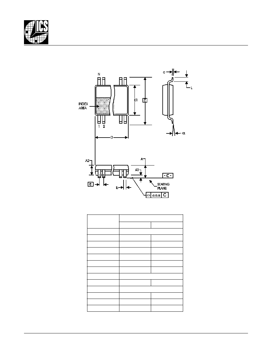
ACKAGE
O
UTLINE
- G S
UFFIX
T
ABLE
8. P
ACKAGE
D
IMENSIONS
Reference Document: JEDEC Publication 95, MO-153
L
O
B
M
Y
S
s
r
e
t
e
m
i
l
l
i
M
m
u
m
i
n
i
M
m
u
m
i
x
a
M
N
0
2
A
-
-
0
2
.
1
1
A
5
0
.
0
5
1
.
0
2
A
0
8
.
0
5
0
.
1
b
9
1
.
0
0
3
.
0
c
9
0
.
0
0
2
.
0
D
0
4
.
6
0
6
.
6
E
C
I
S
A
B
0
4
.
6
1
E
0
3
.
4
0
5
.
4
e
C
I
S
A
B
5
6
.
0
L
5
4
.
0
5
7
.
0
∞
0
∞
8
a
a
a
-
-
0
1
.
0
8737AG-11
www.icst.com/products/hiperclocks.html
REV. A JUNE 3, 2002
13
Integrated
Circuit
Systems, Inc.
ICS8737-11
L
OW
S
KEW
,
∏
1/
∏
2
D
IFFERENTIAL
-
TO
- 3.3V LVPECL C
LOCK
G
ENERATOR
T
ABLE
9. O
RDERING
I
NFORMATION
While the information presented herein has been checked for both accuracy and reliability, Integrated Circuit Systems, Incorporated (ICS) assumes no responsibility for either its use
or for infringement of any patents or other rights of third parties, which would result from its use. No other circuits, patents, or licenses are implied. This product is intended for use
in normal commercial applications. Any other applications such as those requiring extended temperature range, high reliability, or other extraordinary environmental requirements are
not recommended without additional processing by ICS. ICS reserves the right to change any circuitry or specifications without notice. ICS does not authorize or warrant any ICS
product for use in life support devices or critical medical instruments.
r
e
b
m
u
N
r
e
d
r
O
/
t
r
a
P
g
n
i
k
r
a
M
e
g
a
k
c
a
P
t
n
u
o
C
e
r
u
t
a
r
e
p
m
e
T
1
1
-
G
A
7
3
7
8
S
C
I
1
1
-
G
A
7
3
7
8
S
C
I
P
O
S
S
T
d
a
e
l
0
2
2
7
C
∞
0
7
o
t
C
∞
0
T
1
1
-
G
A
7
3
7
8
S
C
I
1
1
-
G
A
7
3
7
8
S
C
I
l
e
e
R
d
n
a
e
p
a
T
n
o
P
O
S
S
T
d
a
e
l
0
2
0
0
5
2
C
∞
0
7
o
t
C
∞
0
8737AG-11
www.icst.com/products/hiperclocks.html
REV. A JUNE 3, 2002
14
Integrated
Circuit
Systems, Inc.
ICS8737-11
L
OW
S
KEW
,
∏
1/
∏
2
D
IFFERENTIAL
-
TO
- 3.3V LVPECL C
LOCK
G
ENERATOR
T
E
E
H
S
Y
R
O
T
S
I
H
N
O
I
S
I
V
E
R
v
e
R
e
l
b
a
T
e
g
a
P
e
g
n
a
h
C
f
o
n
o
i
t
p
i
r
c
s
e
D
e
t
a
D
A
3
.
m
a
r
g
a
i
D
g
n
i
m
i
T
N
E
_
K
L
C
,
1
e
r
u
g
i
F
d
e
t
a
d
p
U
1
0
/
7
1
/
0
1
A
3
.
m
a
r
g
a
i
D
g
n
i
m
i
T
N
E
_
K
L
C
,
1
e
r
u
g
i
F
d
e
s
i
v
e
R
1
0
/
1
3
/
0
1
A
8
.
n
o
i
t
c
e
s
s
t
u
p
t
u
O
L
C
E
P
V
L
r
o
f
n
o
i
t
a
n
i
m
r
e
T
d
e
d
d
A
2
0
/
3
/
6