Document Outline
- General Description
- Features
- Pin Assignment
- Block Diagram
- Simplified Block Diagram
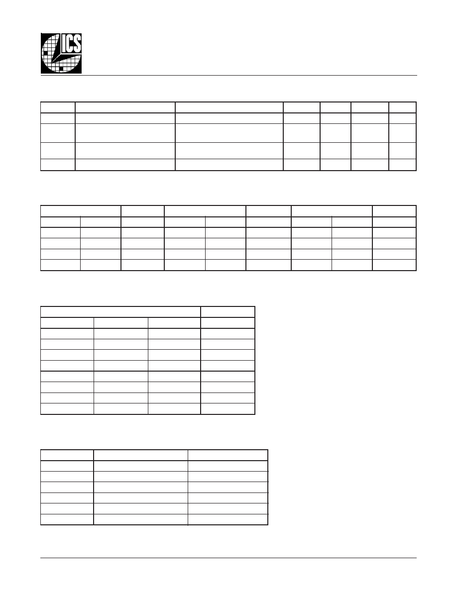
- Pin Descriptions
- Pin Characteristics
- Output Bank Configuration Select Function Table
- Feedback Configuration Select Function Table
- Control Input Select Function Table
- Timing Diagrams
- Absolute Maximum Ratings
- Power Supply DC Characteristics
- Differential DC Characteristics
- Input Frequency Characteristics
- AC Characteristics
- Parameter Measurement Information
- 3.3V Output Load AC Test Circuit Diagram
- Differential Input Level Diagram
- Cycle-to-Cycle Jitter Diagram
- Output Skew Diagram
- Static Phase Offset (Differential) Diagram
- Static Phase Offset (LVCMOS) Diagram
- Output Rise/Fall Time Diagram
- Output Duty Cycle/Pulse Width/Period Diagram
- Application Information
- Using the Output Freeze Circuitry
- Overview
- Protocol
- Freeze Data Input Protocol Diagram
- Output Disable Timing Diagram
- Power Supply
- Wiring the Differential Input to Accept Single Ended Levels
- Differential Clock Input Interface
- HiPerClockS CLK/nCLK Input Driven by ICS HiPerClockS LVHSTL Driver Diagram
- HiPerClockS CLK/nCLK Input Driven by 3.3V LVPECL Driver Diagrams
- HiPerClockS CLK/nCLK Input Driven by 3.3V LVDS Driver Diagram
- Schematic Example
- Reliability Information
- Transistor Count
- Package Outline
- Package Dimensions
- Ordering Information

87973DYI-147
www.icst.com/products/hiperclocks.html
REV. A AUGUST 26, 2003
1
Integrated
Circuit
Systems, Inc.
ICS87973I-147
L
OW
S
KEW
, 1-
TO
-12
LVCMOS / LVTTL C
LOCK
M
ULTIPLIER
/Z
ERO
D
ELAY
B
UFFER
P
IN
A
SSIGNMENT
G
ENERAL
D
ESCRIPTION
The ICS87973I-147 is a LVCMOS/LVTTL clock
generator and a member of the HiPerClockSTM fam-
ily of High Performance Clock Solutions from ICS.
The ICS87973I-147 has three selectable inputs
and provides 14 LVCMOS/LVTTL outputs.
The ICS87973I-147 is a highly flexible device. The three select-
able inputs (1 differential and 2 single ended inputs) are often
used in systems requiring redundant clock sources. Up to three
different output frequencies can be generated among the three
output banks.
The three output banks and feedback output each have their
own output dividers which allows the device to generate a
multitude of different bank frequency ratios and output-to-input
frequency ratios. In addition, 2 outputs in Bank C (QC2, QC3)
can be selected to be inverting or non-inverting. The output fre-
quency range is 10MHz to 150MHz. The input frequency range is
6MHz to 120MHz.
The ICS87973I-147 also has a QSYNC output which can be
used for system synchronization purposes. It monitors Bank A
and Bank C outputs and goes low one period prior to coincident
rising edges of Bank A and Bank C clocks. QSYNC then goes
high again when the coincident rising edges of Bank A and
Bank C occur. This feature is used primarily in applications where
Bank A and Bank C are running at different frequencies, and is
particularly useful when they are running at non-integer mul-
tiples of one another.
Example Applications:
1.
System Clock generator: Use a 16.66MHz reference
clock to generate eight 33.33MHz copies for PCI and
four 100MHz copies for the CPU or PCI-X.
2.
Line Card Multiplier: Multiply differential 62.5MHz from
a back plane to single-ended 125MHz for the line Card
ASICs and Gigabit Ethernet Serdes.
3.
Zero Delay buffer for Synchronous memory: Fan out
up to twelve 100MHz copies from a memory controller
reference clock to the memory chips on a memory module
with zero delay.
F
EATURES
∑ Fully integrated PLL
∑ 14 LVCMOS/LVTTL outputs; (12) clock, (1) feedback, (1) sync
∑ Selectable LVCMOS/LVTTL or differential CLK, nCLK inputs
∑ CLK0, CLK1 can accept the following input levels:
LVCMOS or LVTTL
∑ CLK, nCLK pair can accept the following differential
input levels: LVPECL, LVDS, LVHSTL, SSTL, HCSL
∑ Output frequency range: 10MHz to 150MHz
∑ VCO range: 240MHz to 500MHz
∑ Output skew: 200ps (maximum)
∑ Cycle-to-cycle jitter, (all banks ˜ 4): 55ps (maximum)
∑ Full 3.3V supply voltage
∑ -40∞C to 85∞C ambient operating temperature
∑ Pin compatible with MPC973
∑ Compatible with PowerPCTM and PentiumTM Microprocessors
HiPerClockSTM
ICS
FSEL_FB0
V
DD
QFB
GNDO
EXT_FB
QB3
V
DDO
QB2
GNDO
QB1
V
DDO
QB0
GNDO
40
41
42
43
44
45
46
47
48
49
50
51
52
1 2 3 4 5 6 7 8 9 10 11 12 13
26
25
24
23
22
21
20
19
18
17
16
15
14
39 38 37 36 35 34 33 32 31 30 29 28 27
FSEL_B1
FSEL_B0
FSEL_A1
FSEL_A0
QA3
V
DDO
QA2
GNDO
QA1
V
DDO
QA0
GNDO
VCO_SEL
FSEL_FB1
QSYNC
GNDO
QC0
V
DDO
QC1
FSEL_C0
FSEL_C1
QC2
V
DDO
QC3
GNDO
INV_CLK
V
DDA
nCLK
CLK
CLK1
CLK0
CLK_SEL
REF_SEL
PLL_SEL
FSEL_FB2
FRZ_D
A
T
A
FRZ_CLK
nMR/OE
GNDI
52-Lead LQFP
10mm x 10mm x 1.4mm package body
Y package
Top View
ICS87973I-147

87973DYI-147
www.icst.com/products/hiperclocks.html
REV. A AUGUST 26, 2003
2
Integrated
Circuit
Systems, Inc.
ICS87973I-147
L
OW
S
KEW
, 1-
TO
-12
LVCMOS / LVTTL C
LOCK
M
ULTIPLIER
/Z
ERO
D
ELAY
B
UFFER
SYNC
FRZ
SYNC
FRZ
SYNC
FRZ
SYNC
FRZ
SYNC
FRZ
SYNC
FRZ
SYNC
FRZ
SYNC
FRZ
SYNC
FRZ
SYNC
FRZ
SYNC
FRZ
SYNC
FRZ
VCO_SEL
PLL_SEL
REF_SEL
CLK
nCLK
CLK0
CLK1
CLK_SEL
EXT_FB
FSEL_FB2
nMR/OE
FSEL_A0:1
FSEL_B0:1
FSEL_C0:1
FSEL_FB0:2
FRZ_CLK
FRZ_DATA
INV_CLK
QA0
QA1
QA2
QA3
QB0
QB1
QB2
QB3
QC0
QC1
QC2
QC3
QFB
QSYNC
OUTPUT DISABLE
CIRCUITRY
DATA GENERATOR
12
2
2
2
3
SYNC PULSE
˜4, ˜6, ˜8, ˜12
˜4, ˜6, ˜8, ˜10
˜2, ˜4, ˜6, ˜8
˜2
0
1
0
1
0
1
POWER-ON
RESET
PHASE
DETECTOR
VCO
LPF
SYNC
FRZ
D
Q
D
Q
D
Q
D
Q
D
Q
D
Q
B
LOCK
D
IAGRAM
1
0
˜4, ˜6, ˜8, ˜10

87973DYI-147
www.icst.com/products/hiperclocks.html
REV. A AUGUST 26, 2003
3
Integrated
Circuit
Systems, Inc.
ICS87973I-147
L
OW
S
KEW
, 1-
TO
-12
LVCMOS / LVTTL C
LOCK
M
ULTIPLIER
/Z
ERO
D
ELAY
B
UFFER
S
IMPLIFIED
B
LOCK
D
IAGRAM
0
1
1
0
0
1
˜1
˜2
SYNC
FRZ
SYNC
FRZ
SYNC
FRZ
SYNC
FRZ
SYNC
FRZ
SYNC
FRZ
SYNC
FRZ
SYNC
FRZ
SYNC
FRZ
SYNC
FRZ
SYNC
FRZ
O
UTPUT
D
ISABLE
C
IRCUITRY
0
1
0
1
PLL
VCO R
ANGE
240MHz - 500MHz
SYNC
FRZ
3
2
2
2
INV_CLK
FSEL_A[0:1]
FSEL_B[0:1]
FSEL_C[0:1]
FSEL_FB[0:2]
nMR/OE
0 0 ˜4
0 1 ˜6
1 0 ˜8
1 1 ˜12
FSEL_
A1 A0 QAx
0 0 ˜4
0 1 ˜6
1 0 ˜8
1 1 ˜10
FSEL_
B1 B0 QBx
0 0 0 ˜4
0 0 1 ˜6
0 1 0 ˜8
0 1 1 ˜10
1 0 0 ˜8
1 0 1 ˜12
1 1 0 ˜16
1 1 1 ˜20
FSEL_
FB2 FB1 FB0 QFB
0 0 ˜2
0 1 ˜4
1 0 ˜6
1 1 ˜8
FSEL_
C1 C0 QCx
QA0
QA1
QA2
QA3
QB0
QB1
QB2
QB3
QC0
QC1
QC2
QC3
QFB
QSYNC
CLK
nCLK
CLK0
CLK1
CLK_SEL
REF_SEL
EXT_FB
VCO_SEL
PLL_SEL
FRZ_CLK
FRZ_DATA

87973DYI-147
www.icst.com/products/hiperclocks.html
REV. A AUGUST 26, 2003
4
Integrated
Circuit
Systems, Inc.
ICS87973I-147
L
OW
S
KEW
, 1-
TO
-12
LVCMOS / LVTTL C
LOCK
M
ULTIPLIER
/Z
ERO
D
ELAY
B
UFFER
T
ABLE
1. P
IN
D
ESCRIPTIONS
r
e
b
m
u
N
e
m
a
N
e
p
y
T
n
o
i
t
p
i
r
c
s
e
D
1
I
D
N
G
r
e
w
o
P
.
d
n
u
o
r
g
y
l
p
p
u
s
r
e
w
o
P
2
E
O
/
R
M
n
t
u
p
n
I
p
u
ll
u
P
n
e
h
W
.
s
t
u
p
t
u
o
e
h
t
s
e
l
b
a
n
e
,
H
G
I
H
n
e
h
W
.
e
l
b
a
n
e
t
u
p
t
u
o
d
n
a
t
e
s
e
r
r
e
t
s
a
M
.
y
r
t
i
u
c
r
i
c
e
d
i
v
i
d
t
u
p
t
u
o
s
t
e
s
e
r
d
n
a
e
t
a
t
s
i
r
t
o
t
s
t
u
p
t
u
o
e
h
t
s
t
e
s
e
r
,
W
O
L
.
s
l
e
v
e
l
e
c
a
f
r
e
t
n
i
L
T
T
V
L
/
S
O
M
C
V
L
.
s
t
u
p
t
u
o
ll
a
s
e
l
b
a
s
i
d
d
n
a
s
e
l
b
a
n
E
3
K
L
C
_
Z
R
F
t
u
p
n
I
p
u
ll
u
P
.
s
l
e
v
e
l
e
c
a
f
r
e
t
n
i
L
T
T
V
L
/
S
O
M
C
V
L
.
y
r
t
i
u
c
r
i
c
e
z
e
e
r
f
r
o
f
t
u
p
n
i
k
c
o
l
C
4
A
T
A
D
_
Z
R
F
t
u
p
n
I
p
u
ll
u
P
.
y
r
t
i
u
c
r
i
c
e
z
e
e
r
f
r
o
f
t
u
p
n
i
a
t
a
d
n
o
i
t
a
r
u
g
i
f
n
o
C
.
s
l
e
v
e
l
e
c
a
f
r
e
t
n
i
L
T
T
V
L
/
S
O
M
C
V
L
7
2
,
6
2
,
5
,
2
B
F
_
L
E
S
F
,
1
B
F
_
L
E
S
F
0
B
F
_
L
E
S
F
t
u
p
n
I
p
u
ll
u
P
.
e
u
l
a
v
e
d
i
v
i
D
k
c
a
b
d
e
e
F
l
o
r
t
n
o
c
s
n
i
p
t
c
e
l
e
S
.
s
l
e
v
e
l
e
c
a
f
r
e
t
n
i
L
T
T
V
L
/
S
O
M
C
V
L
6
L
E
S
_
L
L
P
t
u
p
n
I
p
u
ll
u
P
t
u
p
t
u
o
e
h
t
o
t
t
u
p
n
i
e
h
t
s
a
s
k
c
o
l
c
e
c
n
e
r
e
f
e
r
d
n
a
L
L
P
e
h
t
n
e
e
w
t
e
b
s
t
c
e
l
e
S
.
L
L
P
e
h
t
s
e
s
s
a
p
y
b
,
W
O
L
n
e
h
W
.
L
L
P
s
t
c
e
l
e
s
,
H
G
I
H
n
e
h
W
.
s
r
e
d
i
v
i
d
.
s
l
e
v
e
l
e
c
a
f
r
e
t
n
i
L
T
T
V
L
/
S
O
M
C
V
L
7
L
E
S
_
F
E
R
t
u
p
n
I
p
u
ll
u
P
.
s
t
u
p
n
i
K
L
C
n
,
K
L
C
d
n
a
1
K
L
C
r
o
0
K
L
C
n
e
e
w
t
e
b
s
t
c
e
l
e
S
.
1
K
L
C
r
o
0
K
L
C
s
t
c
e
l
e
s
,
W
O
L
n
e
h
W
.
K
L
C
n
,
K
L
C
s
t
c
e
l
e
s
,
H
G
I
H
n
e
h
W
.
s
l
e
v
e
l
e
c
a
f
r
e
t
n
i
L
T
T
V
L
/
S
O
M
C
V
L
8
L
E
S
_
K
L
C
t
u
p
n
I
p
u
ll
u
P
r
o
t
c
e
t
e
d
e
s
a
h
p
s
a
1
K
L
C
d
n
a
0
K
L
C
n
e
e
w
t
e
b
s
t
c
e
l
e
S
.
t
u
p
n
i
t
c
e
l
e
s
k
c
o
l
C
.
1
K
L
C
s
t
c
e
l
e
s
,
H
G
I
H
n
e
h
W
.
0
K
L
C
s
t
c
e
l
e
s
,
W
O
L
n
e
h
W
.
e
c
n
e
r
e
f
e
r
.
s
l
e
v
e
l
e
c
a
f
r
e
t
n
i
L
T
T
V
L
/
S
O
M
C
V
L
0
1
,
9
,
0
K
L
C
1
K
L
C
t
u
p
n
I
p
u
ll
u
P
.
s
l
e
v
e
l
e
c
a
f
r
e
t
n
i
L
T
T
V
L
/
S
O
M
C
V
L
.
s
t
u
p
n
i
k
c
o
l
c
e
c
n
e
r
e
f
e
R
1
1
K
L
C
t
u
p
n
I
p
u
ll
u
P
.
t
u
p
n
i
k
c
o
l
c
l
a
i
t
n
e
r
e
f
f
i
d
g
n
i
t
r
e
v
n
i
-
n
o
N
2
1
K
L
C
n
t
u
p
n
I
V
.
t
u
p
n
i
k
c
o
l
c
l
a
i
t
n
e
r
e
f
f
i
d
g
n
i
t
r
e
v
n
I
D
D
.
g
n
i
t
a
o
l
f
t
f
e
l
n
e
h
w
t
l
u
a
f
e
d
2
/
3
1
V
A
D
D
r
e
w
o
P
.
n
i
p
y
l
p
p
u
s
g
o
l
a
n
A
4
1
K
L
C
_
V
N
I
t
u
p
n
I
p
u
ll
u
P
.
s
t
u
p
t
u
o
3
C
Q
d
n
a
2
C
Q
r
o
f
t
c
e
l
e
s
k
c
o
l
c
d
e
t
r
e
v
n
I
.
s
l
e
v
e
l
e
c
a
f
r
e
t
n
i
L
T
T
V
L
/
S
O
M
C
V
L
,
0
3
,
4
2
,
5
1
1
5
,
7
4
,
9
3
,
5
3
O
D
N
G
r
e
w
o
P
.
d
n
u
o
r
g
y
l
p
p
u
s
r
e
w
o
P
,
8
1
,
6
1
3
2
,
1
2
,
2
C
Q
,
3
C
Q
0
C
Q
,
1
C
Q
t
u
p
t
u
O
7
.
s
t
u
p
t
u
o
k
c
o
l
c
C
k
n
a
B
.
e
c
n
a
d
e
p
m
i
t
u
p
t
u
o
l
a
c
i
p
y
t
.
s
l
e
v
e
l
e
c
a
f
r
e
t
n
i
L
T
T
V
L
/
S
O
M
C
V
L
,
3
3
,
2
2
,
7
1
9
4
,
5
4
,
7
3
V
O
D
D
r
e
w
o
P
.
s
n
i
p
y
l
p
p
u
s
t
u
p
t
u
O
0
2
,
9
1
,
1
C
_
L
E
S
F
0
C
_
L
E
S
F
t
u
p
n
I
p
u
ll
u
P
.
s
l
e
v
e
l
e
c
a
f
r
e
t
n
i
L
T
T
V
L
/
S
O
M
C
V
L
.
s
t
u
p
t
u
o
C
k
n
a
B
r
o
f
s
n
i
p
t
c
e
l
e
S
5
2
C
N
Y
S
Q
t
u
p
t
u
O
,
1
e
r
u
g
i
F
o
t
r
e
f
e
R
.
C
k
n
a
B
d
n
a
A
k
n
a
B
r
o
f
t
u
p
t
u
o
n
o
i
t
a
z
i
n
o
r
h
c
n
y
S
.
s
l
e
v
e
l
e
c
a
f
r
e
t
n
i
L
T
T
V
L
/
S
O
M
C
V
L
.
s
m
a
r
g
a
i
D
g
n
i
m
i
T
8
2
V
D
D
r
e
w
o
P
.
s
n
i
p
y
l
p
p
u
s
e
r
o
C
9
2
B
F
Q
t
u
p
t
u
O
.
s
l
e
v
e
l
e
c
a
f
r
e
t
n
i
L
T
T
V
L
/
S
O
M
C
V
L
.
t
u
p
t
u
o
k
c
o
l
c
k
c
a
b
d
e
e
F
1
3
B
F
_
T
X
E
t
u
p
n
I
p
u
ll
u
P
.
s
l
e
v
e
l
e
c
a
f
r
e
t
n
i
L
T
T
V
L
/
S
O
M
C
V
L
.
k
c
a
b
d
e
e
f
d
e
d
n
e
t
x
E
,
4
3
,
2
3
8
3
,
6
3
,
2
B
Q
,
3
B
Q
0
B
Q
,
1
B
Q
t
u
p
t
u
O
7
.
s
t
u
p
t
u
o
k
c
o
l
c
B
k
n
a
B
.
e
c
n
a
d
e
p
m
i
t
u
p
t
u
o
l
a
c
i
p
y
t
.
s
l
e
v
e
l
e
c
a
f
r
e
t
n
i
L
T
T
V
L
/
S
O
M
C
V
L
1
4
,
0
4
,
1
B
_
L
E
S
F
0
B
_
L
E
S
F
t
u
p
n
I
p
u
ll
u
P
.
s
l
e
v
e
l
e
c
a
f
r
e
t
n
i
L
T
T
V
L
/
S
O
M
C
V
L
.
s
t
u
p
t
u
o
B
k
n
a
B
r
o
f
s
n
i
p
t
c
e
l
e
S
3
4
,
2
4
,
1
A
_
L
E
S
F
0
A
_
L
E
S
F
t
u
p
n
I
p
u
ll
u
P
.
s
l
e
v
e
l
e
c
a
f
r
e
t
n
i
L
T
T
V
L
/
S
O
M
C
V
L
.
s
t
u
p
t
u
o
A
k
n
a
B
r
o
f
s
n
i
p
t
c
e
l
e
S
,
6
4
,
4
4
0
5
,
8
4
,
2
A
Q
,
3
A
Q
0
A
Q
,
1
A
Q
t
u
p
t
u
O
7
.
s
t
u
p
t
u
o
k
c
o
l
c
A
k
n
a
B
.
e
c
n
a
d
e
p
m
i
t
u
p
t
u
o
l
a
c
i
p
y
t
.
s
l
e
v
e
l
e
c
a
f
r
e
t
n
i
L
T
T
V
L
/
S
O
M
C
V
L
2
5
L
E
S
_
O
C
V
t
u
p
n
I
p
u
ll
u
P
.
1
˜
O
C
V
s
t
c
e
l
e
s
,
H
G
I
H
n
e
h
W
.
O
C
V
s
t
c
e
l
e
S
.
s
l
e
v
e
l
e
c
a
f
r
e
t
n
i
L
T
T
V
L
/
S
O
M
C
V
L
.
2
˜
O
C
V
s
t
c
e
l
e
s
,
W
O
L
n
e
h
W
:
E
T
O
N
p
u
ll
u
P
.
s
e
u
l
a
v
l
a
c
i
p
y
t
r
o
f
,
s
c
i
t
s
i
r
e
t
c
a
r
a
h
C
n
i
P
,
2
e
l
b
a
t
e
e
S
.
s
r
o
t
s
i
s
e
r
t
u
p
n
i
l
a
n
r
e
t
n
i
o
t
r
e
f
e
r
87973DYI-147
www.icst.com/products/hiperclocks.html
REV. A AUGUST 26, 2003
5
Integrated
Circuit
Systems, Inc.
ICS87973I-147
L
OW
S
KEW
, 1-
TO
-12
LVCMOS / LVTTL C
LOCK
M
ULTIPLIER
/Z
ERO
D
ELAY
B
UFFER
T
ABLE
2. P
IN
C
HARACTERISTICS
l
o
b
m
y
S
r
e
t
e
m
a
r
a
P
s
n
o
i
t
i
d
n
o
C
t
s
e
T
m
u
m
i
n
i
M
l
a
c
i
p
y
T
m
u
m
i
x
a
M
s
t
i
n
U
C
N
I
e
c
n
a
t
i
c
a
p
a
C
t
u
p
n
I
4
F
p
R
P
U
L
L
U
P
,
R
N
W
O
D
L
L
U
P
r
o
t
s
i
s
e
R
n
w
o
d
ll
u
P
/
p
u
ll
u
P
t
u
p
n
I
1
5
K
C
D
P
e
c
n
a
t
i
c
a
p
a
C
n
o
i
t
a
p
i
s
s
i
D
r
e
w
o
P
)
t
u
p
t
u
o
r
e
p
(
V
D
D
V
,
A
D
D
V
,
O
D
D
V
5
6
4
.
3
=
8
1
F
p
R
T
U
O
e
c
n
a
d
e
p
m
I
t
u
p
t
u
O
5
7
2
1
T
ABLE
3A. O
UTPUT
B
ANK
C
ONFIGURATION
S
ELECT
F
UNCTION
T
ABLE
s
t
u
p
n
I
s
t
u
p
t
u
O
s
t
u
p
n
I
s
t
u
p
t
u
O
s
t
u
p
n
I
s
t
u
p
t
u
O
1
A
_
L
E
S
F
0
A
_
L
E
S
F
A
Q
1
B
_
L
E
S
F
0
B
_
L
E
S
F
B
Q
1
C
_
L
E
S
F
0
C
_
L
E
S
F
C
Q
0
0
4
˜
0
0
4
˜
0
0
2
˜
0
1
6
˜
0
1
6
˜
0
1
4
˜
1
0
8
˜
1
0
8
˜
1
0
6
˜
1
1
2
1
˜
1
1
0
1
˜
1
1
8
˜
T
ABLE
3B. F
EEDBACK
C
ONFIGURATION
S
ELECT
F
UNCTION
T
ABLE
s
t
u
p
n
I
s
t
u
p
t
u
O
2
B
F
_
L
E
S
F
1
B
F
_
L
E
S
F
0
B
F
_
L
E
S
F
B
F
Q
0
0
0
4
˜
0
0
1
6
˜
0
1
0
8
˜
0
1
1
0
1
˜
1
0
0
8
˜
1
0
1
2
1
˜
1
1
0
6
1
˜
1
1
1
0
2
˜
T
ABLE
3C. C
ONTROL
I
NPUT
S
ELECT
F
UNCTION
T
ABLE
n
i
P
l
o
r
t
n
o
C
0
c
i
g
o
L
1
c
i
g
o
L
L
E
S
_
O
C
V
2
/
O
C
V
O
C
V
L
E
S
_
F
E
R
1
K
L
C
r
o
0
K
L
C
K
L
C
n
,
K
L
C
L
E
S
_
K
L
C
0
K
L
C
1
K
L
C
L
E
S
_
L
L
P
L
L
P
S
S
A
P
Y
B
L
L
P
e
l
b
a
n
E
E
O
/
R
M
n
Z
i
H
t
u
p
t
u
O
/
t
e
s
e
R
r
e
t
s
a
M
s
t
u
p
t
u
O
e
l
b
a
n
E
K
L
C
_
V
N
I
3
C
Q
,
2
C
Q
d
e
t
r
e
v
n
I
-
n
o
N
3
C
Q
,
2
C
Q
d
e
t
r
e
v
n
I
87973DYI-147
www.icst.com/products/hiperclocks.html
REV. A AUGUST 26, 2003
6
Integrated
Circuit
Systems, Inc.
ICS87973I-147
L
OW
S
KEW
, 1-
TO
-12
LVCMOS / LVTTL C
LOCK
M
ULTIPLIER
/Z
ERO
D
ELAY
B
UFFER
fVCO
QA
QC
QSYNC
QA
QC
QSYNC
QC(˜2)
QA(˜4)
QSYNC
QC(˜2)
QA(˜8)
QSYNC
QC(˜2)
QA(˜8)
QSYNC
QA(˜6)
QC(˜8)
QSYNC
QA(˜12)
QC(˜2)
QSYNC
F
IGURE
1. T
IMING
D
IAGRAMS
1:1 M
ODE
2:1 M
ODE
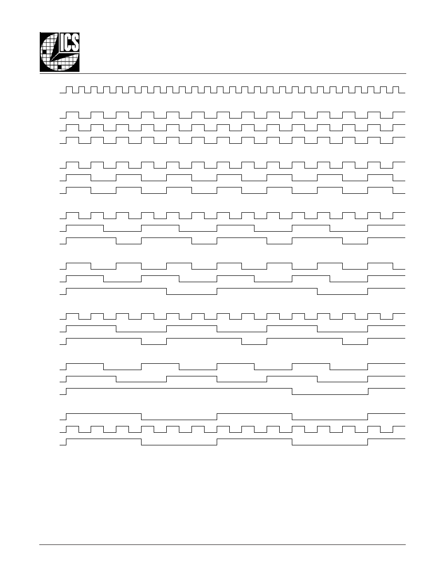
3:1 M
ODE
3:2 M
ODE
4:1 M
ODE
4:3 M
ODE
6:1 M
ODE

87973DYI-147
www.icst.com/products/hiperclocks.html
REV. A AUGUST 26, 2003
7
Integrated
Circuit
Systems, Inc.
ICS87973I-147
L
OW
S
KEW
, 1-
TO
-12
LVCMOS / LVTTL C
LOCK
M
ULTIPLIER
/Z
ERO
D
ELAY
B
UFFER
T
ABLE
4A. P
OWER
S
UPPLY
DC C
HARACTERISTICS
,
V
DD
= V
DDA
= V
DDO
= 3.3V±5%, T
A
= -40∞C
TO
85∞C
l
o
b
m
y
S
r
e
t
e
m
a
r
a
P
s
n
o
i
t
i
d
n
o
C
t
s
e
T
m
u
m
i
n
i
M
l
a
c
i
p
y
T
m
u
m
i
x
a
M
s
t
i
n
U
V
D
D
e
g
a
t
l
o
V
y
l
p
p
u
S
e
r
o
C
5
3
1
.
3
3
.
3
5
6
4
.
3
V
V
A
D
D
e
g
a
t
l
o
V
y
l
p
p
u
S
g
o
l
a
n
A
5
3
9
.
2
3
.
3
5
6
4
.
3
V
V
O
D
D
e
g
a
t
l
o
V
y
l
p
p
u
S
t
u
p
t
u
O
5
3
1
.
3
3
.
3
5
6
4
.
3
V
I
D
D
t
n
e
r
r
u
C
y
l
p
p
u
S
r
e
w
o
P
5
2
2
A
m
I
A
D
D
t
n
e
r
r
u
C
y
l
p
p
u
S
g
o
l
a
n
A
0
2
A
m
.
s
n
o
i
t
a
r
u
g
i
f
n
o
c
e
m
o
s
n
i
d
e
r
i
u
q
e
r
e
b
y
a
m
g
n
il
d
n
a
h
l
a
m
r
e
h
t
l
a
i
c
e
p
S
:
E
T
O
N
l
o
b
m
y
S
r
e
t
e
m
a
r
a
P
s
n
o
i
t
i
d
n
o
C
t
s
e
T
m
u
m
i
n
i
M
l
a
c
i
p
y
T
m
u
m
i
x
a
M
s
t
i
n
U
V
H
I
e
g
a
t
l
o
V
h
g
i
H
t
u
p
n
I
s
t
u
p
n
I
S
O
M
C
V
L
2
V
D
D
3
.
0
+
V
V
L
I
e
g
a
t
l
o
V
w
o
L
t
u
p
n
I
s
t
u
p
n
I
S
O
M
C
V
L
3
.
0
-
8
.
0
V
I
N
I
t
n
e
r
r
u
C
t
u
p
n
I
0
2
1
±
A
µ
V
H
O
e
g
a
t
l
o
V
h
g
i
H
t
u
p
t
u
O
I
H
O
A
m
0
2
-
=
4
.
2
V
V
L
O
e
g
a
t
l
o
V
w
o
L
t
u
p
t
u
O
I
L
O
A
m
0
2
=
5
.
0
V
V
P
P
2
,
1
E
T
O
N
;
e
g
a
t
l
o
V
t
u
p
n
I
k
a
e
P
-
o
t
-
k
a
e
P
K
L
C
n
,
K
L
C
3
.
0
1
V
V
R
M
C
2
,
1
E
T
O
N
;
e
g
a
t
l
o
V
t
u
p
n
I
e
d
o
M
n
o
m
m
o
C
K
L
C
n
,
K
L
C
V
D
D
V
2
-
V
D
D
V
6
.
0
-
V
V
s
a
d
e
n
i
f
e
d
s
i
e
g
a
t
l
o
v
e
d
o
m
n
o
m
m
o
C
:
1
E
T
O
N
H
I
.
l
a
n
g
i
s
l
a
i
t
n
e
r
e
f
f
i
d
e
h
t
f
o
s
n
o
i
t
a
c
il
p
p
a
d
e
d
n
e
e
l
g
n
i
s
r
o
F
.
2
E
T
O
N
,
V
s
i
K
L
C
n
d
n
a
K
L
C
r
o
f
e
g
a
t
l
o
v
t
u
p
n
i
m
u
m
i
x
a
m
e
h
t
D
D
.
V
3
.
0
+
A
BSOLUTE
M
AXIMUM
R
ATINGS
Supply Voltage, V
DD
4.6V
Inputs, V
I
-0.5V to V
DD
+ 0.5 V
Outputs, V
O
-0.5V to V
DDO
+ 0.5V
Package Thermal Impedance,
JA
42.3∞C/W (0 lfpm)
Storage Temperature, T
STG
-65∞C to 150∞C
NOTE: Stresses beyond those listed under Absolute
Maximum Ratings may cause permanent damage to the
device. These ratings are stress specifications only. Functional
operation of product at these conditions or any conditions be-
yond those listed in the
DC Characteristics or AC Character-
istics is not implied. Exposure to absolute maximum rating
conditions for extended periods may affect product reliability.
T
ABLE
4B. D
IFFERENTIAL
DC C
HARACTERISTICS
,
V
DD
= V
DDA
= V
DDO
= 3.3V±5%, T
A
= -40∞C
TO
85∞C
T
ABLE
5. I
NPUT
F
REQUENCY
C
HARACTERISTICS
,
V
DD
= V
DDA
= V
DDO
= 3.3V±5%, T
A
= -40∞C
TO
85∞C
l
o
b
m
y
S
r
e
t
e
m
a
r
a
P
s
n
o
i
t
i
d
n
o
C
t
s
e
T
m
u
m
i
n
i
M
l
a
c
i
p
y
T
m
u
m
i
x
a
M
s
t
i
n
U
f
N
I
y
c
n
e
u
q
e
r
F
t
u
p
n
I
,
1
K
L
C
,
0
K
L
C
1
E
T
O
N
;
K
L
C
n
,
K
L
C
0
2
1
z
H
M
K
L
C
_
Z
R
F
0
2
z
H
M
f
o
e
g
n
a
r
O
C
V
e
h
t
n
i
s
i
"
e
d
i
v
i
D
k
c
a
b
d
e
e
F
*
k
c
o
l
c
"
e
r
u
s
n
e
o
t
o
i
t
a
r
e
d
i
v
i
d
k
c
a
b
d
e
e
f
e
h
t
n
o
s
d
n
e
p
e
d
y
c
n
e
u
q
e
r
f
t
u
p
n
I
:
1
E
T
O
N
.
z
H
M
0
0
5
o
t
z
H
M
0
4
2

87973DYI-147
www.icst.com/products/hiperclocks.html
REV. A AUGUST 26, 2003
8
Integrated
Circuit
Systems, Inc.
ICS87973I-147
L
OW
S
KEW
, 1-
TO
-12
LVCMOS / LVTTL C
LOCK
M
ULTIPLIER
/Z
ERO
D
ELAY
B
UFFER
T
ABLE
6. AC C
HARACTERISTICS
,
V
DD
= V
DDA
= V
DDO
= 3.3V±5%, T
A
= -40∞C
TO
85∞C
l
o
b
m
y
S
r
e
t
e
m
a
r
a
P
s
n
o
i
t
i
d
n
o
C
t
s
e
T
m
u
m
i
n
i
M
l
a
c
i
p
y
T
m
u
m
i
x
a
M
s
t
i
n
U
f
X
A
M
y
c
n
e
u
q
e
r
F
t
u
p
t
u
O
˜2
0
5
1
z
H
M
˜4
5
2
1
z
H
M
˜6
3
3
.
3
8
z
H
M
˜8
5
.
2
6
z
H
M
)
ÿ
(
t
;
t
e
s
f
f
O
e
s
a
h
P
c
i
t
a
t
S
1
E
T
O
N
0
K
L
C
B
F
Q
˜8
z
H
M
0
5
=
y
c
n
e
u
q
e
r
F
n
I
0
1
-
5
4
1
0
0
3
s
p
1
K
L
C
5
6
-
0
9
5
4
2
s
p
K
L
C
n
,
K
L
C
0
3
1
-
8
1
5
6
1
s
p
t
)
o
(
k
s
2
E
T
O
N
;
w
e
k
S
t
u
p
t
u
O
0
0
2
s
p
t
)
c
c
(
t
ij
4
,
3
E
T
O
N
;
r
e
t
t
i
J
e
l
c
y
C
-
o
t
-
e
l
c
y
C
4
˜
s
k
n
a
B
ll
A
5
5
s
p
f
O
C
V
e
g
n
a
R
k
c
o
L
O
C
V
L
L
P
0
4
2
0
0
5
z
H
M
t
K
C
O
L
3
E
T
O
N
;
e
m
i
T
k
c
o
L
L
L
P
0
1
S
m
t
R
t
/
F
e
m
i
T
ll
a
F
/
e
s
i
R
t
u
p
t
u
O
V
2
o
t
V
8
.
0
0
5
1
0
0
7
s
p
c
d
o
e
l
c
y
C
y
t
u
D
t
u
p
t
u
O
5
4
5
5
%
t
L
Z
P
t
,
H
Z
P
3
E
T
O
N
;
e
m
i
T
e
l
b
a
n
E
t
u
p
t
u
O
2
0
1
s
n
t
Z
L
P
t
,
Z
H
P
3
E
T
O
N
;
e
m
I
T
e
l
b
a
s
i
D
t
u
p
t
u
O
2
8
s
n
l
a
n
g
i
s
t
u
p
n
i
k
c
a
b
d
e
e
f
e
g
a
r
e
v
a
e
h
t
d
n
a
k
c
o
l
c
e
c
n
e
r
e
f
e
r
t
u
p
n
i
e
h
t
n
e
e
w
t
e
b
e
c
n
e
r
e
f
f
i
d
e
m
i
t
e
h
t
s
a
d
e
n
i
f
e
D
:
1
E
T
O
N
.
e
l
b
a
t
s
s
i
y
c
n
e
u
q
e
r
f
e
c
n
e
r
e
f
e
r
t
u
p
n
i
e
h
t
d
n
a
d
e
k
c
o
l
s
i
L
L
P
e
h
t
n
e
h
w
.
s
n
o
i
t
i
d
n
o
c
d
a
o
l
l
a
u
q
e
h
t
i
w
d
n
a
e
g
a
t
l
o
v
y
l
p
p
u
s
e
m
a
s
e
h
t
t
a
s
t
u
p
t
u
o
n
e
e
w
t
e
b
w
e
k
s
s
a
d
e
n
i
f
e
D
:
2
E
T
O
N
V
t
a
d
e
r
u
s
a
e
M
O
D
D
.
2
/
.
n
o
i
t
c
u
d
o
r
p
n
i
d
e
t
s
e
t
t
o
N
.
n
o
i
t
a
z
i
r
e
t
c
a
r
a
h
c
y
b
d
e
e
t
n
a
r
a
u
g
e
r
a
s
r
e
t
e
m
a
r
a
p
e
s
e
h
T
:
3
E
T
O
N
.
5
6
d
r
a
d
n
a
t
S
C
E
D
E
J
h
t
i
w
e
c
n
a
d
r
o
c
c
a
n
i
d
e
n
i
f
e
d
s
i
r
e
t
e
m
a
r
a
p
s
i
h
T
:
4
E
T
O
N

87973DYI-147
www.icst.com/products/hiperclocks.html
REV. A AUGUST 26, 2003
9
Integrated
Circuit
Systems, Inc.
ICS87973I-147
L
OW
S
KEW
, 1-
TO
-12
LVCMOS / LVTTL C
LOCK
M
ULTIPLIER
/Z
ERO
D
ELAY
B
UFFER
P
ARAMETER
M
EASUREMENT
I
NFORMATION
3.3V O
UTPUT
L
OAD
AC T
EST
C
IRCUIT
SCOPE
Qx
LVCMOS
1.65V±5%
-1.65V±5%
C
YCLE
-
TO
-C
YCLE
J
ITTER
O
UTPUT
S
KEW
tsk(o)
V
DDO
2
V
DDO
2
Qy
Qx
S
TATIC
P
HASE
O
FFSET
(D
IFFERENTIAL
)
nCLK
EXT_FB
CLK
t(ÿ)
V
DD
2
(where
t(ÿ) is any random sample, and t(ÿ)
mean
is the average
of the sampled cycles measured on controlled edges)
t (ÿ)
mean
= Static Phase Offset
V
CMR
Cross Points
V
PP
nCLK
CLK
GND
V
DD
S
TATIC
P
HASE
O
FFSET
(LVCMOS)
t(ÿ)
V
DD
2
V
DD
2
(where
t(ÿ) is any random sample, and t(ÿ)
mean
is the average
of the sampled cycles measured on controlled edges)
t(ÿ)
mean
= Static Phase Offset
CLK0,
CLK1
EXT_FB
V
DD
,
V
DDA
, V
DDO
GND
D
IFFERENTIAL
I
NPUT
L
EVEL
QA0:QA3,
QB0:QB3,
QC0:QC3,
QSYNC,
QFB
V
DDO
2
V
DDO
2
V
DDO
2
t
cycle n
t
cycle n+1
t
jit(cc) =
t
cycle n ≠
t
cycle n+1
1000 Cycles
Clock
Outputs
0.8V
2V
2V
0.8V
t
R
t
F
O
UTPUT
R
ISE
/F
ALL
T
IME
Pulse Width
t
PERIOD
t
PW
t
PERIOD
odc =
V
DDO
2
QA0:QA3,
QB0:QB3,
QC0:QC3,
QSYNC,
QFB
O
UTPUT
D
UTY
C
YCLE
/ P
ULSE
W
IDTH
P
ERIOD

87973DYI-147
www.icst.com/products/hiperclocks.html
REV. A AUGUST 26, 2003
10
Integrated
Circuit
Systems, Inc.
ICS87973I-147
L
OW
S
KEW
, 1-
TO
-12
LVCMOS / LVTTL C
LOCK
M
ULTIPLIER
/Z
ERO
D
ELAY
B
UFFER
FRZ
Latched
FRZ
C
l
o
cke
d
Qx F
REEZE
Internal
Qx Internal
Qx Out
FRZ_CLK
FRZ_DATA
Star
t
Bit
QA0
QA1
QA2
QA3
QB0
QB1
QB2
QB3
QC1
QC2
QC3 QSYNC
A
PPLICATION
I
NFORMATION
F
IGURE
2A. F
REEZE
D
ATA
I
NPUT
P
ROTOCOL
U
SING
T
HE
O
UTPUT
F
REEZE
C
IRCUITRY
O
VERVIEW
To enable low power states within a system, each output of
ICS87973I-147 (Except QC0 and QFB) can be individually fro-
zen (stopped in the logic "0" state) using a simple serial inter-
face to a 12 bit shift register. A serial interface was chosen to
eliminate the need for each output to have its own Output En-
able pin, which would dramatically increase pin count and pack-
age cost. Common sources in a system that can be used to
drive the ICS87973I-147 serial interface are FPGA's and ASICs.
P
ROTOCOL
The Serial interface consists of two pins, FRZ_Data (Freeze
Data) and FRZ_CLK (Freeze Clock). Each of the outputs which
can be frozen has its own freeze enable bit in the 12 bit shift
register. The sequence is started by supplying a logic "0" start
bit followed by 12NRZ freeze enable bits. The period of each
FRZ_DATA bit equals the period of the FRZ_CLK signal. The
FRZ_DATA serial transmission should be timed so the
ICS87973I-147 can sample each FRZ_DATA bit with the rising
edge of the FRZ_CLK signal. To place an output in the freeze
state, a logic "0" must be written to the respective freeze enable
bit in the shift register. To unfreeze an output, a logic "1" must be
written to the respective freeze enable bit. Outputs will not be-
come enabled/disabled until all 12 data bits are shifted into the
shift register. When all 12 data bits are shifted in the register, the
next rising edge of FRZ_CLK will enable or disable the outputs.
If the bit that is following the 12th bit in the register is a logic "0",
it is used for the start bit of the next cycle; otherwise, the device
will wait and won't start the next cycle until it sees a logic "0" bit.
Freezing and unfreezing of the output clock is synchronous (see
the timing diagram below). When going into a frozen state, the
output clock will go LOW at the time it would normally go LOW,
and the freeze logic will keep the output low until unfrozen. Like-
wise, when coming out of the frozen state, the output will go
HIGH only when it would normally go HIGH. This logic, there-
fore, prevents runt pulses when going into and out of the frozen
state.
F
IGURE
2B. O
UTPUT
D
ISABLE
T
IMING
87973DYI-147
www.icst.com/products/hiperclocks.html
REV. A AUGUST 26, 2003
11
Integrated
Circuit
Systems, Inc.
ICS87973I-147
L
OW
S
KEW
, 1-
TO
-12
LVCMOS / LVTTL C
LOCK
M
ULTIPLIER
/Z
ERO
D
ELAY
B
UFFER
P
OWER
S
UPPLY
F
ILTERING
T
ECHNIQUES
As in any high speed analog circuitry, the power supply pins
are vulnerable to random noise. The ICS87973I-147 provides
separate power supplies to isolate any high switching
noise from the outputs to the internal PLL. V
DD
, V
DDA
, and V
DDO
should be individually connected to the power supply
plane through vias, and bypass capacitors should be
used for each pin. To achieve optimum jitter performance,
power supply isolation is required.
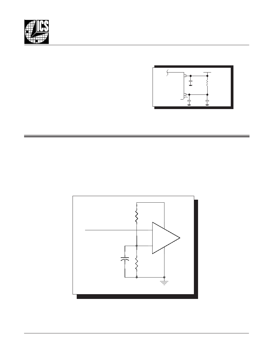
Figure 3 illustrates how
a 10
resistor along with a 10µF and a .01µF bypass
capacitor should be connected to each V
DDA
pin.
F
IGURE
3. P
OWER
S
UPPLY
F
ILTERING
10
V
DDA
10
µF
.01
µF
3.3V
.01
µF
V
DD
Figure 4 shows how the differential input can be wired to accept
single ended levels. The reference voltage V_REF = V
DD
/2 is
generated by the bias resistors R1, R2 and C1. This bias circuit
should be located as close as possible to the input pin. The ratio
F
IGURE
4. S
INGLE
E
NDED
S
IGNAL
D
RIVING
D
IFFERENTIAL
I
NPUT
W
IRING
THE
D
IFFERENTIAL
I
NPUT
TO
A
CCEPT
S
INGLE
E
NDED
L
EVELS
of R1 and R2 might need to be adjusted to position the V_REF in
the center of the input voltage swing. For example, if the input
clock swing is only 2.5V and V
DD
= 3.3V, V_REF should be 1.25V
and R2/R1 = 0.609.
V_REF
R1
1K
C1
0.1u
R2
1K
Single Ended Clock Input
CLK
nCLK
VDD

87973DYI-147
www.icst.com/products/hiperclocks.html
REV. A AUGUST 26, 2003
12
Integrated
Circuit
Systems, Inc.
ICS87973I-147
L
OW
S
KEW
, 1-
TO
-12
LVCMOS / LVTTL C
LOCK
M
ULTIPLIER
/Z
ERO
D
ELAY
B
UFFER
F
IGURE
5C. H
I
P
ER
C
LOCK
S CLK/
N
CLK I
NPUT
D
RIVEN
BY
3.3V LVPECL D
RIVER
F
IGURE
5B. H
I
P
ER
C
LOCK
S CLK/
N
CLK I
NPUT
D
RIVEN
BY
3.3V LVPECL D
RIVER
F
IGURE
5D. H
I
P
ER
C
LOCK
S CLK/
N
CLK I
NPUT
D
RIVEN
BY
3.3V LVDS D
RIVER
3.3V
R1
50
R3
50
Zo = 50 Ohm
LVPECL
Zo = 50 Ohm
HiPerClockS
CLK
nCLK
3.3V
Input
R2
50
Zo = 50 Ohm
Input
HiPerClockS
CLK
nCLK
3.3V
R3
125
R2
84
Zo = 50 Ohm
3.3V
R4
125
LVPECL
R1
84
3.3V
D
IFFERENTIAL
C
LOCK
I
NPUT
I
NTERFACE
The CLK /nCLK accepts LVDS, LVPECL, LVHSTL, SSTL, HCSL
and other differential signals. Both V
SWING
and V
OH
must meet the
V
PP
and V
CMR
input requirements. Figures 5A to 5D show inter-
face examples for the HiPerClockS CLK/nCLK input driven by
the most common driver types. The input interfaces suggested
F
IGURE
5A. H
I
P
ER
C
LOCK
S CLK/
N
CLK I
NPUT
D
RIVEN
BY
ICS H
I
P
ER
C
LOCK
S LVHSTL D
RIVER
here are examples only. Please consult with the vendor of the
driver component to confirm the driver termination requirements.
For example in
Figure 5A, the input termination applies for ICS
HiPerClockS LVHSTL drivers. If you are using an LVHSTL driver
from another vendor, use their termination recommendation.
1.8V
R2
50
Input
LVHSTL Driver
ICS
HiPerClockS
R1
50
LVHSTL
3.3V
Zo = 50 Ohm
Zo = 50 Ohm
HiPerClockS
CLK
nCLK
Zo = 50 Ohm
R1
100
3.3V
LVDS_Driv er
Zo = 50 Ohm
Receiv er
CLK
nCLK
3.3V

87973DYI-147
www.icst.com/products/hiperclocks.html
REV. A AUGUST 26, 2003
13
Integrated
Circuit
Systems, Inc.
ICS87973I-147
L
OW
S
KEW
, 1-
TO
-12
LVCMOS / LVTTL C
LOCK
M
ULTIPLIER
/Z
ERO
D
ELAY
B
UFFER
S
CHEMATIC
E
XAMPLE
Figure 6 shows a schematic example of using ICS87973I-147.
This example shows general design of input, output termination,
logic control input pull up/down and power supply filtering. In
this example, the clock input is driven by an LVCMOS driver.
C8
0.1uF
R3
43
C3
0.1uF
RS
Zo = 50
C11
0.01u
RD1
Not Install
C16
10u
(U1-45)
VDD
C7
0.1uF
RU2
Not Install
VDD
C9
0.1uF
R5
1K
(U1-28)
VDD=3.3V
C6
0.1uF
VDD
(U1-37)
R6
1K
R2
43
Serial Clcok
To Logic
Input
pins
Zo = 50
Set Logic
Input to
'0'
R1
43
To Logic
Input
pins
VDD
R10
1K
C5
0.1uF
R9
1K
(U1-22)
(U1-49)
(U1-33)
Zo = 50
Set Logic
Input to
'1'
U1
ICS87973I-147
1
2
3
4
5
6
7
8
9
10
11
12
13
14
15
16
17
18
19
20
21
22
23
24
25
26
39
38
37
36
35
34
33
32
31
30
29
28
27
52
51
50
49
48
47
46
45
44
43
42
41
40
GNDI
nMR/OE
FRZ_CLK
FRZ_DATA
FSEL_FB2
PLL_SEL
REF_SEL
CLK_SEL
CLK0
CLK1
CLK
nCLK
VDDA
IN
V
_
C
L
K
G
NDO
QC
3
V
DDO
QC
2
F
S
E
L_C
1
F
S
E
L_C
0
QC
1
V
DDO
QC
0
G
NDO
Q
SYN
C
F
S
E
L_F
B
1
GNDO
QB0
VDDO
QB1
GNDO
QB2
VDDO
QB3
EXT_FB
GNDO
QFB
VDD
FSEL_FB0
VC
O
_
SE
L
GN
D
O
QA
0
VD
D
O
QA
1
GN
D
O
QA
2
VD
D
O
QA
3
FS
E
L
_
A
0
FS
E
L
_
A
1
FS
E
L
_
B
0
FS
E
L
_
B
1
VDD
VDD
Logic Input Pin Examples
RD2
1K
R7
10 - 15
(U1-17)
RU1
1K
R8
1K
Serial Data
Zo = 50
R4
1K
C4
0.1uF
LVCMOS CLOCK
VDD
F
IGURE
6. ICS87973I-147 S
CHEMATIC
E
XAMPLE

87973DYI-147
www.icst.com/products/hiperclocks.html
REV. A AUGUST 26, 2003
14
Integrated
Circuit
Systems, Inc.
ICS87973I-147
L
OW
S
KEW
, 1-
TO
-12
LVCMOS / LVTTL C
LOCK
M
ULTIPLIER
/Z
ERO
D
ELAY
B
UFFER
R
ELIABILITY
I
NFORMATION
T
RANSISTOR
C
OUNT
The transistor count for ICS87973I-147 is: 8364
T
ABLE
7.
JA
VS
. A
IR
F
LOW
T
ABLE
FOR
52 L
EAD
LQFP
JA
by Velocity (Linear Feet per Minute)
0
200
500
Single-Layer PCB, JEDEC Standard Test Boards
58.0∞C/W
47.1∞C/W
42.0∞C/W
Multi-Layer PCB, JEDEC Standard Test Boards
42.3∞C/W
36.4∞C/W
34.0∞C/W
NOTE: Most modern PCB designs use multi-layered boards. The data in the second row pertains to most designs.

87973DYI-147
www.icst.com/products/hiperclocks.html
REV. A AUGUST 26, 2003
15
Integrated
Circuit
Systems, Inc.
ICS87973I-147
L
OW
S
KEW
, 1-
TO
-12
LVCMOS / LVTTL C
LOCK
M
ULTIPLIER
/Z
ERO
D
ELAY
B
UFFER
T
ABLE
8. P
ACKAGE
D
IMENSIONS
Reference Document: JEDEC Publication 95, MS-026
P
ACKAGE
O
UTLINE
- Y S
UFFIX
FOR
52 L
EAD
LQFP
N
O
I
T
A
I
R
A
V
C
E
D
E
J
S
R
E
T
E
M
I
L
L
I
M
N
I
S
N
O
I
S
N
E
M
I
D
L
L
A
L
O
B
M
Y
S
C
C
B
M
U
M
I
N
I
M
L
A
N
I
M
O
N
M
U
M
I
X
A
M
N
2
5
A
-
-
-
-
0
6
.
1
1
A
5
0
.
0
-
-
5
1
.
0
2
A
5
3
.
1
0
4
.
1
5
4
.
1
b
2
2
.
0
2
3
.
0
8
3
.
0
c
9
0
.
0
-
-
0
2
.
0
D
C
I
S
A
B
0
0
.
2
1
1
D
C
I
S
A
B
0
0
.
0
1
E
C
I
S
A
B
0
0
.
2
1
1
E
C
I
S
A
B
0
0
.
0
1
e
C
I
S
A
B
5
6
.
0
L
5
4
.
0
-
-
5
7
.
0
0
∞
-
-
7
∞
c
c
c
-
-
-
-
8
0
.
0
87973DYI-147
www.icst.com/products/hiperclocks.html
REV. A AUGUST 26, 2003
16
Integrated
Circuit
Systems, Inc.
ICS87973I-147
L
OW
S
KEW
, 1-
TO
-12
LVCMOS / LVTTL C
LOCK
M
ULTIPLIER
/Z
ERO
D
ELAY
B
UFFER
T
ABLE
9. O
RDERING
I
NFORMATION
While the information presented herein has been checked for both accuracy and reliability, Integrated Circuit Systems, Incorporated (ICS) assumes no responsibility for either its use or
for infringement of any patents or other rights of third parties, which would result from its use. No other circuits, patents, or licenses are implied. This product is intended for use in normal
commercial and industrial applications. Any other applications such as those requiring high reliability, or other extraordinary environmental requirements are not recommended without
additional processing by ICS. ICS reserves the right to change any circuitry or specifications without notice. ICS does not authorize or warrant any ICS product for use in life support devices
or critical medical instruments.
r
e
b
m
u
N
r
e
d
r
O
/
t
r
a
P
g
n
i
k
r
a
M
e
g
a
k
c
a
P
t
n
u
o
C
e
r
u
t
a
r
e
p
m
e
T
7
4
1
-
I
Y
D
3
7
9
7
8
S
C
I
7
4
1
I
D
3
7
9
7
S
C
I
P
F
Q
L
d
a
e
L
2
5
y
a
r
t
r
e
p
0
6
1
C
∞
5
8
o
t
C
∞
0
4
-
T
7
4
1
-
I
Y
D
3
7
9
7
8
S
C
I
7
4
1
I
D
3
7
9
7
S
C
I
l
e
e
R
d
n
a
e
p
a
T
n
o
P
F
Q
L
d
a
e
L
2
5
0
0
5
C
∞
5
8
o
t
C
∞
0
4
-