
www.icst.com/products/hiperclocks.html
Aug 02, 2002
1
Integrated
Circuit
Systems, Inc.
HiPerClockSTM
Application Note
3.3V LVPECL D
RIVER
T
ERMINATION
This application note provides termination examples for HiPerClockS
TM
3.3V LVPECL drivers. The HiPerClockS
TM
3.3V LVPECL driver is an open source/emitter driver as shown in Figure 1. Proper termination is required to
ensure proper function of the device and signal integrity. There are many different termination schemes for the
LVPECL drivers. This application note includes standard direct termination and AC coupled termination. The
following termination approaches are only general recommendations under ideal conditions. Board designers
should consult with their signal integrity engineers or verify through simulations in their system environment. The
trace length and physical location of the components can affect signal integrity. The 50-Ohm transmission lines
in the following diagrams indicate whether the components should be located near the driver or near the
receiver.
P.C. Board
VCCO
VCCO
Zo = 50
Q
VCCO-2V
R1
VEE
R3
50
nQ
Zo = 50
R4
50
LVPECL Driver
R2
Figure 1 HiPerClockS
TM
LVPECL driver
Direct LVPECL Termination
The standard 3.3V LVPECL termination is shown in Figure 2. This termination scheme is used in
characterization. The draw back of using this termination scheme in real applications is that it requires an
additional power supply V
CCO
-2V = 1.3V. In actual applications, the terminations shown in Figure 3 and Figure 4
are commonly used. These termination approaches eliminate the need of 1.3V power supply. In Figure 5, R1
and R2 located near the driver serve as current paths for the LVPECL outputs. The R3=100 Ohm located near
the receiving serves as matched load termination for the transmission lines.

www.icst.com/products/hiperclocks.html
Aug 02, 2002
2
Integrated
Circuit
Systems, Inc.
HiPerClockSTM
Application Note
3.3V LVPECL D
RIVER
T
ERMINATION
Zo = 50
Td
Zo = 50
Td
+
-
R2
50
VCCO-2V
VEE
VCCO=VEE+3.3V
R1
50
Figure 2 Standard 3.3V LVPECL Termination
+
-
Zo = 50
Td
3.3V
Zo = 50
Td
VCCO =3.3V
R1
125
R2
84
R4
84
R3
125
Figure 3 Equivalent 3.3V LVPECL Termination

www.icst.com/products/hiperclocks.html
Aug 02, 2002
3
Integrated
Circuit
Systems, Inc.
HiPerClockSTM
Application Note
3.3V LVPECL D
RIVER
T
ERMINATION
VCCO=3.3V
+
-
R2
50
Zo = 50
Td
R3
50
R1
50
Zo = 50
Td
Figure 4 Equivalent 3.3V LVPECL Termination
R1
100-180
TL1
Zo = 50
Td
VCCO=3.3V
R3
100
3v3 PECL Driver
U1
R2
100-180
nTL1
Zo = 50
Td
+
-
Figure 5 Termination with 100-Ohm resistor across the differential input

www.icst.com/products/hiperclocks.html
Aug 02, 2002
4
Integrated
Circuit
Systems, Inc.
HiPerClockSTM
Application Note
3.3V LVPECL D
RIVER
T
ERMINATION
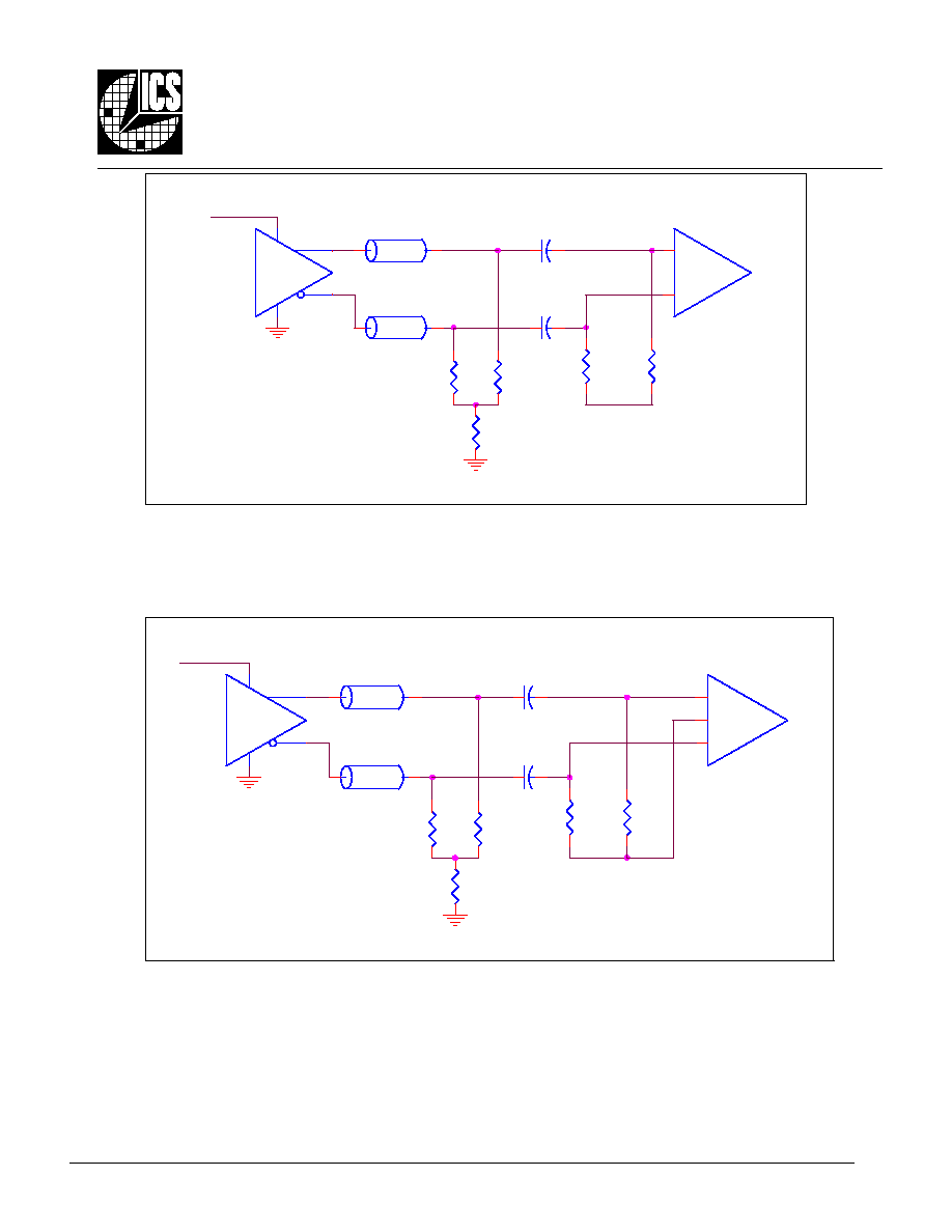
AC Coupled Termination
For AC termination, the offset level needs to be taken care of after the AC capacitors. A bias circuit might be
required. The board design engineer needs to verify what type of receiver is being driven. A few examples of AC
couple termination are shown in this section.
In Figure 6, the R3 and R4 at the driver pins provide a current path for the LVPECL driver. R1 and R2 serve as
matched load termination. The power supply V
BB
controls the offset level so that the signal offset fall within the
VCMR input requirement of the receiver. Figure 7 and Figure 8 are equivalent to Figure 5. The Figure 7 is
equivalent to V
BB
=V
CC
-2V. This offset is suitable for interfacing with HiPerClockS
TM
CLK/nCLK input. Figure 8 is
equivalent to V
BB
=V
CC
-1.3V. This offset is suitable for interfacing with HiPerClockS
TM
PCLK/nPCLK input. Figure 9
shows AC termination with the offset bias voltage V
BB
provided at the receiving end. Figure 10 shows AC
termination with the offset bias voltage V
BB
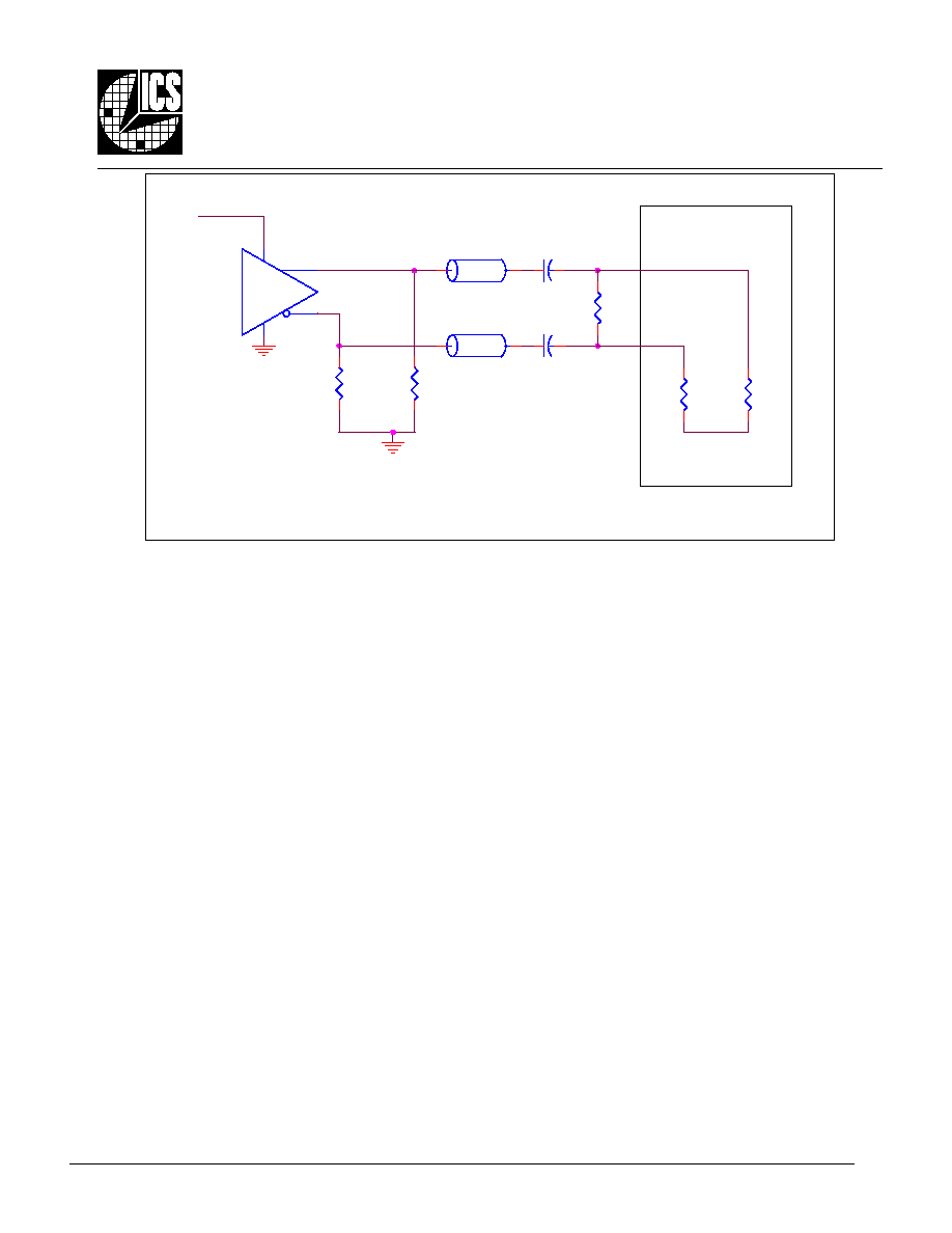
provided by the receiver device. In some cases, for the receiver with
built-in bias resistors R1 and R2, the termination is shown in Figure 11.
R3
100-180
C2
nTL1
Zo = 50
Td
+
-
VCCO=3.3V
R4
100-180
VBB
R2
50
C1
TL1
Zo = 50
Td
R1
50
3v3 PECL Driver
U1
Figure 6 AC Coupled with V
BB
power supply provided at the receiving end

www.icst.com/products/hiperclocks.html
Aug 02, 2002
5
Integrated
Circuit
Systems, Inc.
HiPerClockSTM
Application Note
3.3V LVPECL D
RIVER
T
ERMINATION
nTL1
Zo = 50
Td
R3
125
3.3V
R5
125
R2
100-180
TL1
Zo = 50
Td
3v3 PECL Driver
U1
+
-
C1
C2
R6
84
R4
84
R1
100-180
VCCO=3.3V
Figure 7 AC Coupled with bias offset at V
CC
- 2V (Suitable for interface with HiPerClockS
CLK/nCLK input)
R2
100-180
R6
125
+
-
R1
100-180
C2
R4
125
TL1
Zo = 50
Td
C1
R3
84
3v3 PECL Driver
U1
VCCO=3.3V
3.3V
R5
84
nTL1
Zo = 50
Td
Figure 8 AC coupled with bias offset at V
CC
- 1.3V (Suitable for AC Couple with ICS
HiPerClockS PCLK/nPCLK input)
www.icst.com/products/hiperclocks.html
Aug 02, 2002
6
Integrated
Circuit
Systems, Inc.
HiPerClockSTM
Application Note
3.3V LVPECL D
RIVER
T
ERMINATION
R4
50
R3
50
VBB
+
-
VCCO=3.3V
Zo = 50
Td
R5
50
Zo = 50
Td
R1
1K
C1
R2
1K
C2
Figure 9 AC Coupled Termination with V
BB
bias level provided at the receiver
R4
50
R1
1K
Zo = 50
Td
R5
50
C1
R3
50
R2
1K
C2
VCCO=3.3V
+
-
VBB
Zo = 50
Td
VBB
Figure 10 AC Coupled Termination with V
BB
bias provided by the receiver
www.icst.com/products/hiperclocks.html
Aug 02, 2002
7
Integrated
Circuit
Systems, Inc.
HiPerClockSTM
Application Note
3.3V LVPECL D
RIVER
T
ERMINATION
TL1
Zo = 50
Td
R4
> 1K
C1
R3
> 1K
C2
Receiver
nTL1
Zo = 50
Td
3v3 PECL Driver
U1
R5
100
R3
100-180
R4
100-180
VCCO=3.3V
VBB
Figure 11 AC coupled for the receiver with built-in bias circuit