 | –≠–ª–µ–∫—Ç—Ä–æ–Ω–Ω—ã–π –∫–æ–º–ø–æ–Ω–µ–Ω—Ç: ICS90C65M | –°–∫–∞—á–∞—Ç—å:  PDF PDF  ZIP ZIP |
90C65ARevA111095
Dual Voltage Video/Memory Clock Generator
Introduction
The Integrated Circuit Systems ICS90C65 is a dual clock
generator for VGA applications. It simultaneously generates
two clocks. One clock is for the video memory, and the other
is the video dot clock.
The ICS90C65 has been specifically designed to serve the
portable PC market with operation at either 3.3V or 5V with a
comprehensive power-saving shut-down mode.
This data sheet supplies sales order information, a functional
overview, signal pin details, a block diagram, AC/DC charac-
teristics, timing diagrams, and package mechanical information.
Description
The Integrated Circuit Systems Video Graphics Array Clock
Generator (ICS90C65) is capable of producing different out-
put frequencies under firmware control. The video output
frequency is derived from a 14.318 MHz system clock avail-
able in IBM PC/XT/AT and Personal System/2 computers. It
is designed to work with Western Digital Imaging Video
Graphics Array and 8514/A devices to optimize video subsys-
tem performance.
Features
∑
∑
Specified for dual voltage operation (V
DD
=3.3V or 5V),
but operates continuously from 3.0V to 5.25V
∑
∑
Designed to be powered-down for extended battery life
∑
∑
Backward compatibility to the ICS90C64 and ICS90C63
∑
∑
Dual Clock generator for the IBM-compatible Western
Digital Imaging Video Graphics Array (VGA) LSI
devices, and 8514/A chip sets
∑
∑
Integral loop filter components, reduce cost and phase
jitter
∑
∑
Generates fifteen video clock frequencies (including
25.175 and 28.322 MHz) derived from a 14.318 MHz
system clock reference frequency
∑
∑
On-chip generation of eight memory clock frequencies
∑
∑
Video clock is selectable among the 15 internally gener-
ated clocks and one external clock
∑
∑
CMOS technology
∑
∑
Available in 20-pin PLCC, SOIC and DIP packages
Integrated
Circuit
Systems, Inc.
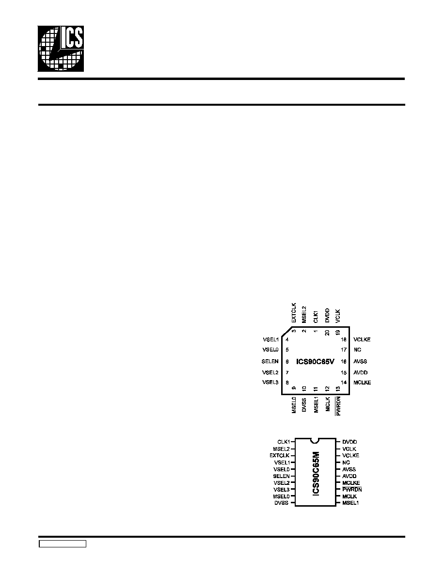
Note:ICS90C65N (DIP) pin-out is identical to ICS90C65M (SOIC) pin-out.
ICS90C65
The video dot clock output may be one of 15 internally-
generated frequencies or one external input. The selection of
the video dot clock frequency is done through four inputs.
∑
∑
VSEL0
∑
∑
VSEL1
∑
∑
VSEL2
∑
∑
VSEL3
VSEL0 and VSEL1 are latched by the SELEN signal. VSEL2
and VSEL3 are used as direct inputs to the VCLK selection.
Table 1-1 is the truth table for VCLK selection.
The input and truth table have been designed to allow a direct
connection to one of the many Western Digital Imaging VGA
controllers or 8514/A chip sets.
The MCLK output is one of eight internally-generated frequen-
cies as shown in Table 1-2. The various VCLK and MCLK
frequencies are derived from the 14.318 MHz input frequency.
The VCLKE and MCLKE input can tristate the VCLK and
MCLK outputs to facilitate board level testing.
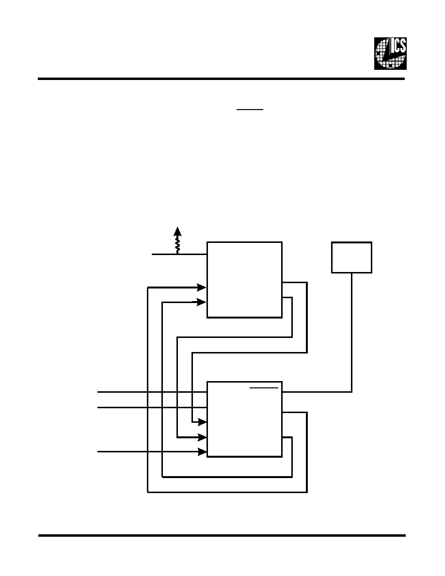
ICS90C65 VGA Interface
The ICS90C65 has two system interfaces: System Bus and
VGA Controller, as well as other programmable inputs. Figure
1 shows how the Integrated Circuit Systems's VGA Clock
ICS90C65 is connected to a VGA controller. Western Digital
Imaging VGA controllers normally have a status bit that indi-
cates to the VGA controller that it is working with a clock chip.
When working with a clock chip the VGA controller changes
t wo of i ts cl ock in pu ts to ou tpu ts. They are
theVCLK1/VCSLD/VCSEL and VCLK2/VCSEL/VCSELH
outputs and they are used to select the required video frequency.
Figure 1
When the power-down capabilities are used, the control signal
for PWRDN is normally held in one of a group of latches. If
the power-down function is not to be used, PWRDN must be
tied to V
DD
, otherwise the internal pull-down will place the chip
in the power-down mode.
VSEL0
14.318
MHz
SD3
SD2
pull-up at reset
and PR15(5)=0
AMD(3)
VCKIN
MCLK
VCSEL
VCS
ICS90C65
WD90C26
LATCH
VSEL1
VSEL2
VCLK
MC
SELEN
CLK1
PWRDN
ICS90C65
2

Inputs from VGA Controller
The VGA controller input to the ICS90C65 is:
∑
∑
SELEN
The ICS90C65 is programmed to generate different video
clock frequencies using the inputs of VSEL0, VSEL1, VSEL2,
and VSEL3. The signals VSEL2 and VSEL3 may be supplied
by the VGA controller as is the case in Western Digital Imaging
VGA controllers. The inputs VSEL0-1 are latched with the
signal SELEN. The SELEN input should be an active low
pulse. This active low pulse is generated in Western Digital
Imaging VGA controllers during I/O writes to internal register
3C2h.
Note: Only VSEL0 and VSEL1 are latched with signal SELEN.
Outputs to VGA Controller
The outputs from the ICS90C65 to the VGA controller are:
∑
∑
MCLK
∑
∑
VCLK
MCLK and VCLK are the two clock outputs to the VGA
controller.
User-Definable Inputs
The user definable inputs are:
∑
∑
EXTCLK
∑
∑
VLCKE, MCLKE
∑
∑
MSELO-2
∑
∑
VSEL2, VSEL3
∑
∑
PWRDN
EXTCLK is an additional input that may be internally routed
to the VCLK output. This additional input is useful for support-
ing modes that require frequencies not provided by the
ICS90C65 or for use during board test.
VCLKE and MCLKE are the output enable signals for VCLK
and MCLK. When low the respective output is tristated.
MSEL0-2 are the memory clock (MCLK) select lines. Ta-
ble 1-2 shows how MCLK frequencies are selected. All signals
in this group have internal pull-up resistors.
VSEL2 and VSEL3 are video clock (VCLK) select lines that
can select additional VCLK frequencies. See Table 1-1.
VSEL2 and VSEL3 have internal pull-ups.
PWRDN can place the ICS90C65 in a power-down mode
which drops its supply current requirement below 1 microamp.
When placed in this mode, the digital inputs may be either high
or low or floating without causing an increase in the ICS90C65
supply current.
The PWRDN pin must be low (It has an internal pull-down.)
in order to place the device in its low power state. The output
pins (VCLK and MCLK) are driven high by the ICS90C65
when it is in its low power state.
If CLKI is being driven by an external source, it may be driven
low or high without a power penalty. If CLKI is at an interme-
diate voltage (V
SS
+0.5 < V
IN
<V
DD
-0.5), there will be a small
increase in supply current. If CLKI is driven at 14.318 MHz
while the chip is in power-down, the ICS90C65 supply current
will increase to approximately 1.2 mA.
The SELEN (pin 6) may be used to guard against inadvertent
frequency changes during power-down/powerup sequences.
By holding the SELEN low during power-down and power-up
sequences, the ICS90C65 will retain the most recent video
frequency selection.
Analog Filters
The analog filters are integral to the ICS90C65 device. No
external components are required. This feature reduces PC
board space requirements and component costs. Phase-jitter is
reduced as externally-generated noise cannot easily influence
the phase-locked loop filter.
System Bus Inputs
The system bus inputs are:
∑
∑
CLKI
∑
∑
VSEL0
∑
∑
VSEL1
The ICS90C65 uses the system bus 14.318 MHz clock as a
reference to generate all its frequencies for both video and
memory clocks. Data lines D2 and D3 are commonly used as
inputs to VSEL0 and VSEL1 for video frequency selection.
ICS90C65
3
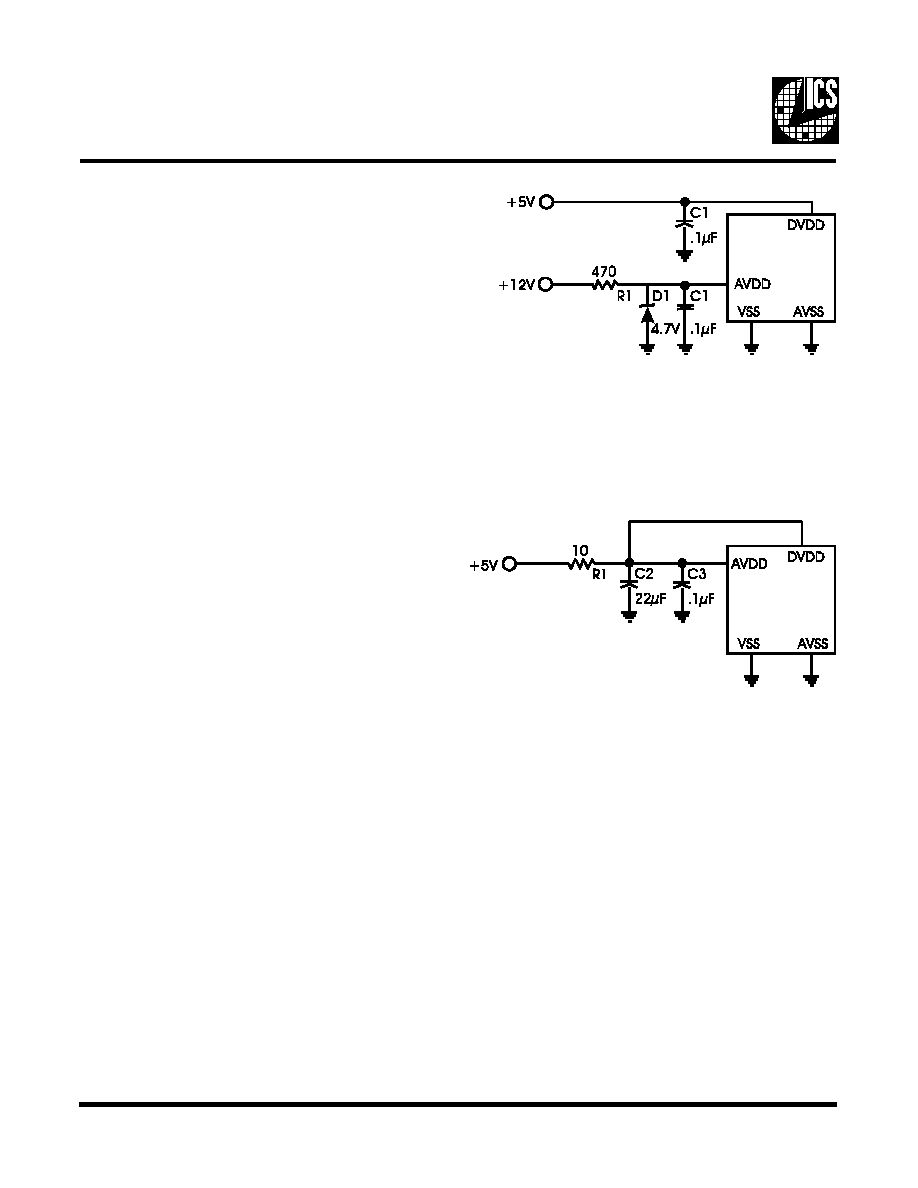
Power Considerations
The ICS90C65 product requires an AV
DD
supply free of fast
rise time transients. This requirement may be met in several
ways and is highly dependent on the characteristics of the host
system. A VGA adapter card is unique in that it must function
in an unknown environment. +5 volt power quality is depend-
ent not only on the quality of the power supply resident in the
host system, but also on the other cards plugged into the host's
backplane. Power supply noise ranges from fair to terrible. As
the VGA adapter manufacturer has no control over this, he must
assume the worst. The best solution is to create a clean +5 volts
by deriving it from the +12 volt supply by using a zener diode
and dropping resistor. A 470 Ohm resistor and 5.1 volt
Zener
diode are the least costly way to accomplish this. A .047 to .1
microfarad bypass capacitor tied from AV
DD
to Av
SS
insures
good high- frequency decoupling of this point.
Laptop and notebook computers have entirely different prob-
lems with power. Typically they have no +12 volt supply;
however, they are much quieter electrically. Because the de-
signer has complete control of the system architecture, he can
place sensitive components and systems such as the RAMDAC
and Dual Video/Memory Clock away from DRAM and other
noise-generating components. Most systems provide power
that is clean enough to allow for jitter-free Dual Video/Memory
Clock performance if the +5 volt supply is decoupled with a
resistor and 22 microfarad Tantalum capacitor. Digital inputs
that are desired to be held at a static logical high level should
not be tied to +5 volts as this may result in excessive current
drain through the ESD protection diode. The internal pull-up
resistors will adequately keep these inputs high.
ICS90C65
4
Pin Descriptions
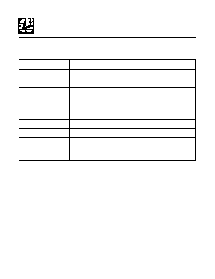
The following table provides the pin descriptions for the 20-pin ICS90C65 packages.
PIN
NUMBER
PIN
SYMBOL
TYPE
DESCRIPTION
1
CLKI
IN
Reference input clock from system.
2
MSEL2
IN
Select input for MCLK selection.
3
EXTCLK
IN
External clock input for an additional frequency.
4
VSEL1
IN
Control input for VCLK selection.
5
VSEL0
IN
Control input for VCLK selection.
6
SELEN
IN
Strobe for latching VSEL(0,1) (low enable).
7
VSEL2
IN
Control input for VCLK selection.
8
VSEL3
IN
Control input for VCLK selection.
9
MSEL0
IN
Select input for MCLK selection.
10
DVSS
-
Ground for Digital Circuit.
11
MSEL1
IN
Select input for MCLK selection.
12
MCLK
OUT
Memory Clock Output.
13
PWRDN
IN
Power Down Control.
14
MCLKE
IN
Enable input for MCLK output (high enables output).
15
AVDD
-
Power supply for analog circuit.
16
AVSS
-
Ground for analog circuit.
17
NC
-
No connection.
18
VCLKE
IN
Enable input for VCLK output (high enables output).
19
VCLK
OUT
Video Clock Output.
20
DVDD
-
Power supply for Digital Circuit.
Note:
CLKI, EXTCLK,VSEL0, VSEL1,VSEL2, VSEL3, SELEN, MSEL0, MSEL1, MSEL2, VCLKE, and MCLKE - input pins have
internal pull-up resistors. PWRDN has an internal pull-down resistor.
ICS90C65
5