ICS9112-18
Zero Delay, Low Skew Buffer
MDS 9112-18 F
1
Revision 050400
Printed 11/15/00
Integrated Circuit Systems, Inc.∑ 525 Race Street ∑ San Jose ∑ CA ∑ 95126 ∑ (408)295-9800tel∑ www.icst.com
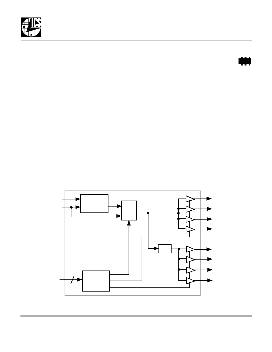
Block Diagram
Description
Features
The ICS9112-18 is a low jitter, low-skew, high
performance PLL based zero delay buffer for high
speed applications. Based on ICS's proprietary low
jitter Phase Locked Loop (PLL) techniques, the
device provides eight low skew outputs at speeds
up to 160 MHz at 3.3 V. The ICS9112-18
includes a bank of four outputs running at 1X, and
another four outputs running at 1/2X. In the zero
delay mode, the rising edge of the input clock is
aligned with the rising edges of all eight outputs.
Compared to competitive CMOS devices, the
ICS9112-18 has the lowest jitter of all.
ICS manufactures the largest variety of clock
generators and buffers, and is the largest clock
supplier in the world.
∑ Packaged in 16 pin narrow SOIC
∑ Zero input-output delay
∑ Four 1X outputs plus four half-X outputs
∑ Output to output skew is less than 250 ps
∑ Output clocks up to 160 MHz at 3.3 V
∑ Ability to generate 2X the input
∑ Full CMOS outputs with 18 mA output drive
capability at TTL levels at 3.3 V
∑ Spread SmartTM technology works with spread
spectrum clock generators
∑ Advanced, low power, sub-micron CMOS process
∑ 3.0 to 5.5 V operating voltage
PLL
CLKA1
FBIN
Mux
CLKA2
S2, S1
2
˜ 2
CLKA3
CLKA4
CLKB1
CLKB2
CLKB3
CLKB4
Control
Logic
CLKIN
ICS9112-18
Zero Delay, Low Skew Buffer
MDS 9112-18 F
2
Revision 050400
Printed 11/15/00
Integrated Circuit Systems, Inc.∑ 525 Race Street ∑ San Jose ∑ CA ∑ 95126 ∑ (408)295-9800tel∑ www.icst.com
Pin Descriptions
Key: I = Input; O = output; P = power supply connection.
Pin Assignment
ICS9112-18
External Components
The ICS9112-18 requires a minimum number of external components for proper operation. Decoupling
capacitors of 0.1µF should be connected between VDD and GND on pins 4 and 5, and VDD and GND
on pins 13 and 12, as close to the device as possible. A series termination resistor of 33
may be used close
to the pin for each clock output to reduce reflections.
16
15
14
13
16 pin narrow (150 mil) SOIC
12
11
10
9
1
2
3
4
5
6
7
8
CLKA1
GND
FBIN
CLKIN
VDD
S2
CLKB1
CLKB2
VDD
GND
CLKB3
S1
CLKB4
CLKA4
CLKA3
CLKA2
S2
S1
Clocks A1-A4
Clocks B1-B4
Internal Generation
PLL Status
0
0
Tri-state (high impedance)
Tri-state (high impedance)
None
On
0
1
Running
Tri-state (high impedance)
PLL
On
1
0
Running
Running
Buffer Only (no zero delay)
Off
1
1
Running
Running
PLL
On
Feedback From
CLKA1:A4
CLKB1:B4
Bank A
CLKIN
CLKIN/2
Bank B
2XCLKIN
CLKIN
Number
Name
Type
Description
1
CLKIN
I
CLocK INput. Connect to input clock source.
2, 3, 14, 15
CLKA1:4
O
CLocK A bank of four outputs.
4, 13
VDD
P
Power supply. Connect both pins to same voltage (either 3.3V or 5V).
5, 12
GND
P
Connect to ground.
6, 7, 10, 11
CLKB1:4
O
CLocK B bank of four outputs. These are low skew divide by two of bank A.
8
S2
I
Select input #2. Selects mode for outputs per table above.
9
S1
I
Select input #1. Selects mode for outputs per table above.
16
FBIN
I
FeedBack INput. Determines outputs per Feedback Configuration Table above.
Output Clock Mode Select Table
Feedback Configuration Table
ICS9112-18
Zero Delay, Low Skew Buffer
MDS 9112-18 F
3
Revision 050400
Printed 11/15/00
Integrated Circuit Systems, Inc.∑ 525 Race Street ∑ San Jose ∑ CA ∑ 95126 ∑ (408)295-9800tel∑ www.icst.com
Parameter
Conditions
Minimum
Typical
Maximum
Units
ABSOLUTE MAXIMUM RATINGS (note 1)
ABSOLUTE MAXIMUM RATINGS (note 1)
Supply voltage, VDD
Referenced to GND
-0.5
7
V
Inputs and Clock Outputs
Referenced to GND
-0.5
VDD+0.5
V
Electrostatic Discharge
MIL-STD-883
2000
V
Ambient Operating Temperature
0
70
∞C
Soldering Temperature
Max of 10 seconds
260
∞C
Junction temperature
150
∞C
Storage temperature
-65
150
∞C
DC CHARACTERISTICS (VDD = 3.3 V unless specified otherwise)
DC CHARACTERISTICS (VDD = 3.3 V unless specified otherwise)
DC CHARACTERISTICS (VDD = 3.3 V unless specified otherwise)
Operating Voltage, VDD
3.00
5.50
V
Input High Voltage, VIH, CLKIN pin only
VDD/2+1
VDD/2
V
Input Low Voltage, VIL, CLKIN pin only
VDD/2
VDD/2-1
V
Input High Voltage, VIH
2
V
Input Low Voltage, VIL
0.8
V
Output High Voltage, VOH
IOH=-18 mA
2.4
V
Output Low Voltage, VOL
IOL=18 mA
0.4
V
Output High Voltage, VOH, CMOS level
IOH=-5 mA
VDD-0.4
V
Operating Supply Current, IDD (Note 2)
No Load, S1 = S2 = 1
44
mA
Short Circuit Current
Each output
±65
mA
Input Capacitance
S2, S1, FBIN
7
pF
AC CHARACTERISTICS (VDD = 3.3 V unless specified otherwise)
AC CHARACTERISTICS (VDD = 3.3 V unless specified otherwise)
AC CHARACTERISTICS (VDD = 3.3 V unless specified otherwise)
Input Clock Frequency
FBIN to CLKA1, S1=S2=1
20
160
MHz
Output Clock Frequency
FBIN to CLKA1, S1=S2=1
20
160
MHz
Output Clock Rise Time, CL=30pF
0.8 to 2.0V
1.5
ns
Output Clock Fall Time, CL=30pF
2.0 to 0.8V
1.5
ns
Output Clock Duty Cycle, VDD=3.3V
At 1.4V
40
50
60
%
Device to Device Skew, equally loaded
rising edges at VDD/2
700
ps
Output to Output Skew, equally loaded
rising edges at VDD/2
250
ps
Maximum Absolute Jitter
300
ps
Cycle to Cycle Jitter, 30pF loads
66.67 MHz outputs
500
ps
Electrical Specifications
Notes:
1. Stresses beyond those listed under Absolute Maximum Ratings could cause permanent damage to the device. Prolonged
exposure to levels above the operating limits but below the Absolute Maximums may affect device reliability.
2. With CLKIN = 160 MHz, FBIN to CLKA1
Using Spread Spectrum Input Clocks
The ICS9112-18 uses ICS' Spread Smart technology, allowing it to accurately track (pass through) any
clocks that use spread spectrum techniques.
ICS9112-18
Zero Delay, Low Skew Buffer
MDS 9112-18 F
4
Revision 050400
Printed 11/15/00
Integrated Circuit Systems, Inc.∑ 525 Race Street ∑ San Jose ∑ CA ∑ 95126 ∑ (408)295-9800tel∑ www.icst.com
While the information presented herein has been checked for both accuracy and reliability, Integrated Circuit Systems, Incorporated (ICS) assumes no responsibility for either its
use or for the infringement of any patents or other rights of third parties, which would result from its use. No other circuits, patents, or licenses are implied. This product is
intended for use in normal commercial applications. Any other applications such as those requiring extended temperature range, high reliability, or other extraordinary
environmental requirements are not recommended without additional processing by ICS. ICS reserves the right to change any circuitry or specifications without notice. ICS does
not authorize or warrant any ICS product for use in life support devices or critical medical instruments.
Ordering Information
Part/Order Number
Marking*
Shipping packaging
Package
Temperature
ICS9112BM-18
9112BM-18
tubes
16 pin SOIC
0-70 ∞C
ICS9112BM-18T
9112BM-18
tape and reel
16 pin SOIC
0-70 ∞C
*Also indicated on the top of the package are the initials ICS in a box.
16 pin SOIC narrow
Inches
Inches
Millimeters
Millimeters
Symbol
Min
Max
Min
Max
A
0.0532
0.0688
1.35
1.75
A1
0.0040
0.0098
0.10
0.24
B
0.0130
0.0200
0.33
0.51
C
0.0075
0.0098
0.19
0.24
D
0.3859
0.3937
9.80
10.00
E
0.1497
0.1574
3.80
4.00
e
.050 BSC
.050 BSC
1.27 BSC
1.27 BSC
H
0.2284
0.2440
5.80
6.20
h
0.0099
0.0195
0.25
0.50
L
0.0160
0.0500
0.41
1.27
Package Outline and Package Dimensions
(
For current dimensional specifications, see JEDEC Publication No. 95.)
B
D
E
H
e
A1
C
A
h x 45∞
L
INDEX
AREA
1
2