Integrated
Circuit
Systems, Inc.
General Description
Features
ICS9112-16
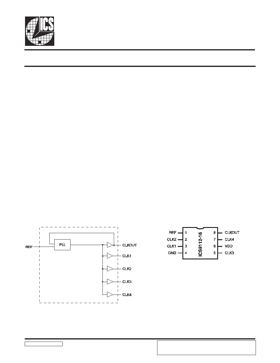
Block Diagram
Low Skew Output Buffer
9112-16 Rev G 02/06/02
Pin Configuration
∑
Zero input - output delay
∑
Frequency range 25 - 133 MHz (3.3V)
∑
High loop filter bandwidth ideal for Spread
Spectrum applications.
∑
Less than 200 ps Jitter between outputs
∑
Skew controlled outputs
∑
Skew less than 250 ps between outputs
∑
Available in 8 pin 150 mil SOIC
or 173 mil TSSOP package.
∑
3.3V ±10% operation
The ICS9112-16 is a high performance, low skew, low jitter
clock driver. It uses a phase lock loop (PLL) technology to
align, in both phase and frequency, the REF input with the
CLKOUT signal. It is designed to distribute high speed
clocks in PC systems operating at speeds from 25 to
133 MHz.
ICS9112-16 is a zero delay buffer that provides
synchronization between the input and output. The
synchronization is established via CLKOUT feed back to the
input of the PLL. Since the skew between the input and
output is less than +/- 350 pS, the part acts as a zero delay
buffer.
The ICS9112-16 comes in an eight pin 150 mil SOIC or 173
mil TSSOP package. It has five output clocks. In the absence
of REF input, will be in the power down mode. In this mode,
the PLL is turned off and the output buffers are pulled low.
Power down mode provides the lowest power consumption
for a standby condition.
8 pin SOIC, TSSOP
ICS reserves the right to make changes in the device data identified in
this publication without further notice. ICS advises its customers to
obtain the latest version of all device data to verify that any
information being relied upon by the customer is current and accurate.

2
ICS9112-16
Pin Descriptions
Notes:
1.
Guaranteed by design and characterization. Not subject to 100% test.
2.
Weak pull-down
3.
Weak pull-down on all outputs
R
E
B
M
U
N
N
I
P
E
M
A
N
N
I
P
E
P
Y
T
N
O
I
T
P
I
R
C
S
E
D
1
F
E
R
2
N
I
.
y
c
n
e
u
q
e
r
f
e
c
n
e
r
e
f
e
r
t
u
p
n
I
2
2
K
L
C
3
T
U
O
t
u
p
t
u
o
k
c
o
l
c
d
e
r
e
f
f
u
B
3
1
K
L
C
3
T
U
O
t
u
p
t
u
o
k
c
o
l
c
d
e
r
e
f
f
u
B
4
D
N
G
R
W
P
d
n
u
o
r
G
5
3
K
L
C
3
T
U
O
t
u
p
t
u
o
k
c
o
l
c
d
e
r
e
f
f
u
B
6
D
D
V
R
W
P
)
V
3
.
3
(
y
l
p
p
u
S
r
e
w
o
P
7
4
K
L
C
3
T
U
O
t
u
p
t
u
o
k
c
o
l
c
d
e
r
e
f
f
u
B
8
T
U
O
K
L
C
3
T
U
O
n
i
p
s
i
h
t
n
o
k
c
a
b
d
e
e
f
l
a
n
r
e
t
n
I
.
t
u
p
t
u
o
k
c
o
l
c
d
e
r
e
f
f
u
B
3
ICS9112-16
Notes:
1.
Guaranteed by design and characterization. Not subject to 100% test.
2.
All Skew specifications are mesured with a 50
transmission line, load teminated with 50
to 1.4V.
3.
Duty cycle measured at 1.4V.
4.
Skew measured at 1.4V on rising edges. Loading must be equal on outputs.
Absolute Maximum Ratings
Supply Voltage . . . . . . . . . . . . . . . . . . . . . . . . . . 7.0 V
Logic Inputs . . . . . . . . . . . . . . . . . . . . . . . . . . . . GND ≠0.5 V to V
DD
+0.5 V
Ambient Operating Temperature . . . . . . . . . . 0∞C to +70∞C
Storage Temperature . . . . . . . . . . . . . . . . . . . . . ≠65∞C to +150∞C
Electrical Characteristics at 3.3V
V
DD
= 3.0 ≠ 3.6 V, T
A
= 0 ≠ 70
∞
C unless otherwise stated
Stresses above those listed under Absolute Maximum Ratings may cause permanent damage to the device. These ratings
are stress specifications only and functional operation of the device at these or any other conditions above those listed
in the operational sections of the specifications is not implied. Exposure to absolute maximum rating conditions for
extended periods may affect product reliability.
s
c
i
t
s
i
r
e
t
c
a
r
a
h
C
C
D
R
E
T
E
M
A
R
A
P
L
O
B
M
Y
S
S
N
O
I
T
I
D
N
O
C
T
S
E
T
N
I
M
P
Y
T
X
A
M
S
T
I
N
U
e
g
a
t
l
o
V
w
o
L
t
u
p
n
I
V
L
I
8
.
0
V
e
g
a
t
l
o
V
h
g
i
H
t
u
p
n
I
V
H
I
0
.
2
V
t
n
e
r
r
u
C
w
o
L
t
u
p
n
I
I
L
I
V
N
I
V
0
=
9
1
0
.
0
5
A
µ
t
n
e
r
r
u
C
h
g
i
H
t
u
p
n
I
I
H
I
V
N
I
V
=
D
D
0
1
.
0
0
.
0
0
1
A
µ
e
g
a
t
l
o
V
w
o
L
t
u
p
t
u
O
1
V
L
O
I
L
O
A
m
5
2
=
5
2
.
0
4
.
0
V
e
g
a
t
l
o
V
h
g
i
H
t
u
p
t
u
O
1
V
H
O
I
H
O
A
m
5
2
=
4
.
2
9
.
2
V
y
l
p
p
u
S
n
w
o
D
r
e
w
o
P
t
n
e
r
r
u
C
I
D
D
z
H
M
0
=
F
E
R
3
.
0
0
.
0
5
A
µ
t
n
e
r
r
u
C
y
l
p
p
u
S
I
D
D
L
E
S
z
H
M
6
6
.
6
6
t
a
s
t
u
t
u
o
d
e
d
a
o
l
n
U
V
t
a
s
t
u
p
n
i
D
D
D
N
G
r
o
0
.
0
3
0
.
0
4
A
m
4
ICS9112-16
Switching Characteristics
Notes:
1.
Guaranteed by design and characterization. Not subject to 100% test.
2.
REF input has a threshold voltage of 1.4V
3.
All parameters expected with loaded outputs
R
E
T
E
M
A
R
A
P
L
O
B
M
Y
S
N
O
I
T
I
D
N
O
C
N
I
M
P
Y
T
X
A
M
S
T
I
N
U
d
o
i
r
e
p
t
u
p
t
u
O
1
t
F
p
0
3
=
L
C
h
t
i
W
0
0
.
0
4
)
5
2
(
5
.
7
)
3
3
1
(
s
n
)
z
H
M
(
d
o
i
r
e
p
t
u
p
n
I
1
t
F
p
0
3
=
L
C
h
t
i
W
0
0
.
0
4
)
5
2
(
5
.
7
)
3
3
1
(
s
n
)
z
H
M
(
e
l
c
y
C
y
t
u
D
1
1
t
D
F
p
0
3
=
L
C
;
V
4
.
1
t
a
d
e
r
u
s
a
e
M
0
.
0
4
0
5
0
6
%
e
l
c
y
C
y
t
u
D
1
2
t
D
z
H
M
6
.
6
6
<
t
u
o
F
2
/
D
D
V
t
a
d
e
r
u
s
a
e
M
5
4
0
5
5
5
%
e
m
i
T
e
s
i
R
1
1
r
t
:
V
0
.
2
d
n
a
V
8
.
0
n
e
e
w
t
e
b
d
e
r
u
s
a
e
M
F
p
0
3
=
L
C
2
.
1
5
.
1
s
n
e
m
i
T
l
l
a
F
1
1
f
t
;
V
8
.
0
d
n
a
V
0
.
2
n
e
e
w
t
e
b
d
e
r
u
s
a
e
M
F
p
0
3
=
L
C
2
.
1
5
.
1
s
n
g
n
i
s
i
R
F
E
R
,
y
a
l
e
D
T
U
O
K
L
C
o
t
e
g
d
E
e
g
d
E
g
n
i
s
i
R
,
1 2
1
r
D
V
4
.
1
t
a
d
e
r
u
s
a
e
M
0
0
5
3
±
s
p
t
u
p
t
u
O
o
t
t
u
p
t
u
O
w
e
k
S
1
w
e
k
s
T
F
p
0
2
=
L
C
,
d
e
d
a
o
l
y
l
l
a
u
q
e
s
t
u
p
t
u
o
l
l
A
0
5
2
s
p
e
c
i
v
e
D
o
t
e
c
i
v
e
D
w
e
k
S
1
k
s
d
T
-
k
s
d
T
T
U
O
K
L
C
e
h
t
n
o
2
/
D
D
V
t
a
d
e
r
u
s
a
e
M
s
e
c
i
v
e
d
f
o
s
n
i
p
0
0
0
7
s
p
r
e
t
t
i
J
e
l
c
y
C
o
t
e
l
c
y
C
1
c
y
c
T
-
c
y
c
T
d
e
d
a
o
l
,
z
H
M
6
6
.
6
6
t
a
d
e
r
u
s
a
e
M
s
t
u
p
t
u
o
0
0
2
s
p
e
m
i
T
k
c
o
L
L
L
P
1
K
C
O
L
t
k
c
o
l
c
d
i
l
a
v
,
y
l
p
p
u
s
r
e
w
o
p
e
l
b
a
t
S
n
i
p
F
E
R
n
o
d
e
t
n
e
s
e
r
p
0
.
1
s
m
r
e
t
t
i
J
e
t
u
l
o
s
b
A
;
r
e
t
t
i
J
1
s
b
a
j
T
s
e
l
c
y
c
0
0
0
,
0
1
@
F
p
0
3
=
L
C
0
0
1
-
0
7
0
0
1
s
p
a
m
g
i
S
-
1
;
r
e
t
t
i
J
1
s
1
j
T
s
e
l
c
y
c
0
0
0
,
0
1
@
F
p
0
3
=
L
C
4
1
0
3
s
p
5
ICS9112-16
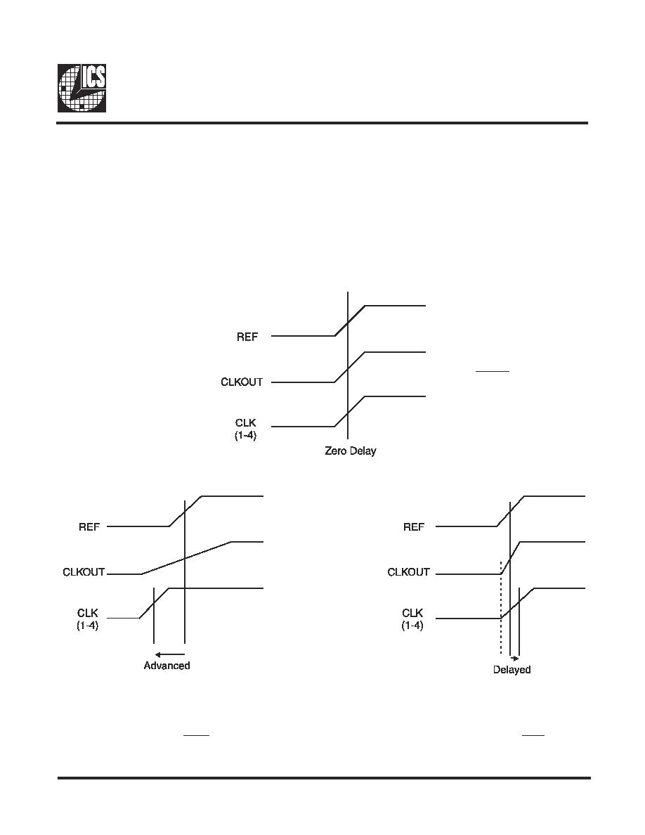
Output to Output Skew
The skew between CLKOUT and the CLK(1-4) outputs is not dynamically adjusted by the PLL. Since CLKOUT is one of the
inputs to the PLL, zero phase difference is maintained from REF to CLKOUT. If all outputs are equally loaded, zero phase
difference will maintained from REF to all outputs.
If applications requiring zero output-output skew, all the outputs must equally loaded.
If the CLK(1-4) outputs are less loaded than CLKOUT, CLK(1-4) outputs will lead it; and if the CLK(1-4) is more loaded than
CLKOUT, CLK(1-4) will lag the CLKOUT.
Since the CLKOUT and the CLK(1-4) outputs are identical, they all start at the same time, but different loads cause them to
have different rise times and different times crossing the measurement thresholds.
REF input and
all outputs
loaded Equally
REF input and CLK(1-4)
outputs loaded equally, with
CLKOUT loaded More.
REF input and CLK(1_4)
outputs loaded equally, with
CLKOUT loaded Less.
Timing diagrams with different loading configurations

6
ICS9112-16
ICS reserves the right to make changes in the device data identified in
this publication without further notice. ICS advises its customers to
obtain the latest version of all device data to verify that any
information being relied upon by the customer is current and accurate.
ICS XXXX y M - PPP - T
Ordering Information
ICS9112yM-16-T
Designation for tape and reel packaging
Pattern Number (2 or 3 digit number for parts with ROM code patterns)
Package Type
M=SOIC
Revision Designator (will not correlate with datasheet revision)
Device Type (consists of 3 or 4 digit numbers)
Prefix
ICS, AV = Standard Device
Example:
SEATING
PLANE
SEATING
PLANE
A1
B
A
e
.10 (.004)
.10 (.004)
h x 45∞
h x 45∞
L
C
INDEX
AREA
INDEX
AREA
1 2
1 2
N
D
E
H
150 mil (Narrow Body) SOIC
MIN
MAX
MIN
MAX
A
1.35
1.75
.0532
.0688
A1
0.10
0.25
.0040
.0098
B
0.33
0.51
.013
.020
C
0.19
0.25
.0075
.0098
D
E
3.80
4.00
.1497
.1574
e
H
5.80
6.20
.2284
.2440
h
0.25
0.50
.010
.020
L
0.40
1.27
.016
.050
N
0∞
8∞
0∞
8∞
VARIATIONS
MIN
MAX
MIN
MAX
8
4.80
5.00
.1890
.1968
10-0030
0.050 BASIC
SYMBOL
In Millimeters
In Inches
COMMON DIMENSIONS COMMON DIMENSIONS
Reference Doc.: JEDEC Publication 95, MS-012
SEE VARIATIONS
SEE VARIATIONS
N
D mm.
D (inch)
SEE VARIATIONS
SEE VARIATIONS
1.27 BASIC

7
ICS9112-16
Ordering Information
ICS9112yG-16-T
Designation for tape and reel packaging
Pattern Number (2 or 3 digit number for parts with ROM code patterns)
Package Type
G=TSSOP
Revision Designator (will not correlate with datasheet revision)
Device Type (consists of 3 or 4 digit numbers)
Prefix
ICS, AV = Standard Device
Example:
ICS XXXX y G - PPP - T
4.40 mm. Body, 0.65 mm. pitch TSSOP
(173 mil)
(0.0256 Inch)
INDEX
AREA
INDEX
AREA
1 2
1 2
N
D
E1
E
SEATING
PLANE
SEATING
PLANE
A1
A
A2
e
- C -
- C -
b
c
L
aaa
C
MIN
MAX
MIN
MAX
A
--
1.20
--
.047
A1
0.05
0.15
.002
.006
A2
0.80
1.05
.032
.041
b
0.19
0.30
.007
.012
c
0.09
0.20
.0035
.008
D
E
E1
4.30
4.50
.169
.177
e
L
0.45
0.75
.018
.030
N
0∞
8∞
0∞
8∞
aaa
--
0.10
--
.004
VARIATIONS
MIN
MAX
MIN
MAX
8
2.90
3.10
.114
.122
10-0035
SYMBOL
In Millimeters
In Inches
COMMON DIMENSIONS
COMMON DIMENSIONS
SEE VARIATIONS
SEE VARIATIONS
6.40 BASIC
0.252 BASIC
0.65 BASIC
0.0256 BASIC
SEE VARIATIONS
SEE VARIATIONS
N
D mm.
D (inch)
Reference Doc.: JEDEC Publication 95, MO-153