Äîêóìåíòàöèÿ è îïèñàíèÿ www.docs.chipfind.ru
Integrated
Circuit
Systems, Inc.
General Description
Features
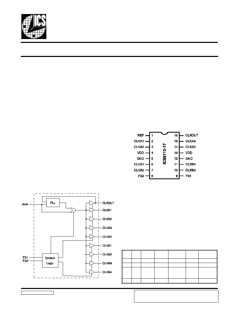
ICS9112-17
Block Diagram
Low Skew Output Buffer
9112-17 Rev G 10/20/00
Pin Configuration
·
Zero input - output delay
·
Frequency range 25 - 133 MHz (3.3V)
·
High loop filter bandwidth ideal for Spread Spectrum
applications.
·
Less than 200 ps cycle to cycle Jitter
·
Skew controlled outputs
·
Skew less than 250 ps between outputs
·
Available in 16 pin, 150 mil SSOP & SOIC package
The ICS9112-17 is a high performance, low skew, low jitter
zero delay buffer. It uses a phase lock loop (PLL) technology
to align, in both phase and frequency, the REF input with the
CLKOUT signal. It is designed to distribute high speed
clocks in PC systems operating at speeds from 25 to
133 MHz.
ICS9112-17 is a zero delay buffer that provides
synchronization between the input and output. The
synchronization is established via CLKOUT feed back to the
input of the PLL. Since the skew between the input and
output is less than +/- 350 pS, the part acts as a zero delay
buffer.
The ICS9112-17 has two banks of four outputs controlled by
two address lines. Depending on the selected address line,
bank B or both banks can be put in a tri-state mode. In this
mode, the PLL is still running and only the output buffers are
put in a high impedance mode. The test mode shuts off the
PLL and connects the input directly to the output buffers (see
table below for functionality).
The ICS9112-17 comes in a sixteen pin 150 mil SOIC or 16
pin SSOP package. In the absence of REF input, will be in the
power down mode. In this mode, the PLL is turned off and the
output buffers are pulled low. Power down mode provides
the lowest power consumption for a standby condition.
2
S
F
1
S
F
A
K
L
C
)
4
,
1
(
B
K
L
C
)
4
,
1
(
T
U
O
K
L
C
t
u
p
t
u
O
e
c
r
u
o
S
L
L
P
n
w
o
d
t
u
h
S
0
0
e
t
a
t
s
i
r
T
e
t
a
t
s
i
r
T
n
e
v
i
r
D
L
L
P
N
0
1
n
e
v
i
r
D
e
t
a
t
s
i
r
T
n
e
v
i
r
D
L
L
P
N
1
0
L
L
P
s
s
a
p
y
B
e
d
o
M
L
L
P
s
s
a
p
y
B
e
d
o
M
L
L
P
s
s
a
p
y
B
e
d
o
M
F
E
R
Y
1
1
n
e
v
i
r
D
n
e
v
i
r
D
n
e
v
i
r
D
L
L
P
N
Functionality
ICS reserves the right to make changes in the device data identified in
this publication without further notice. ICS advises its customers to
obtain the latest version of all device data to verify that any
information being relied upon by the customer is current and accurate.
16 pin SSOP & SOIC
2
ICS9112-17
Pin Descriptions
Notes:
1.
Guaranteed by design and characterization. Not subject to 100% test.
2.
Weak pull-down
3.
Weak pull-down on all outputs
4.
Weak pull-ups on these inputs
R
E
B
M
U
N
N
I
P
E
M
A
N
N
I
P
E
P
Y
T
N
O
I
T
P
I
R
C
S
E
D
1
F
E
R
2
N
I
.
y
c
n
e
u
q
e
r
f
e
c
n
e
r
e
f
e
r
t
u
p
n
I
2
1
A
K
L
C
3
T
U
O
A
k
n
a
B
,
t
u
p
t
u
o
k
c
o
l
c
d
e
r
e
f
f
u
B
3
2
A
K
L
C
3
T
U
O
A
k
n
a
B
,
t
u
p
t
u
o
k
c
o
l
c
d
e
r
e
f
f
u
B
3
1
,
4
D
D
V
R
W
P
)
V
3
.
3
(
y
l
p
p
u
S
r
e
w
o
P
2
1
,
5
D
N
G
R
W
P
d
n
u
o
r
G
6
1
B
K
L
C
3
T
U
O
B
k
n
a
B
.
t
u
p
t
u
o
k
c
o
l
c
d
e
r
e
f
f
u
B
7
2
B
K
L
C
3
T
U
O
B
k
n
a
B
.
t
u
p
t
u
o
k
c
o
l
c
d
e
r
e
f
f
u
B
8
2
S
F
4
N
I
2
t
i
b
,
t
u
p
n
i
t
c
e
l
e
S
9
1
S
F
4
N
I
1
t
i
b
,
t
u
p
n
i
t
c
e
l
e
S
0
1
3
B
K
L
C
3
T
U
O
B
k
n
a
B
.
t
u
p
t
u
o
k
c
o
l
c
d
e
r
e
f
f
u
B
1
1
4
B
K
L
C
3
T
U
O
B
k
n
a
B
.
t
u
p
t
u
o
k
c
o
l
c
d
e
r
e
f
f
u
B
4
1
3
A
K
L
C
3
T
U
O
A
k
n
a
B
,
t
u
p
t
u
o
k
c
o
l
c
d
e
r
e
f
f
u
B
5
1
4
A
K
L
C
3
T
U
O
A
k
n
a
B
,
t
u
p
t
u
o
k
c
o
l
c
d
e
r
e
f
f
u
B
6
1
T
U
O
K
L
C
3
T
U
O
n
i
p
s
i
h
t
n
o
k
c
a
b
d
e
e
f
l
a
n
r
e
t
n
i
,
t
u
p
t
u
o
k
c
o
l
c
d
e
r
e
f
f
u
B
3
ICS9112-17
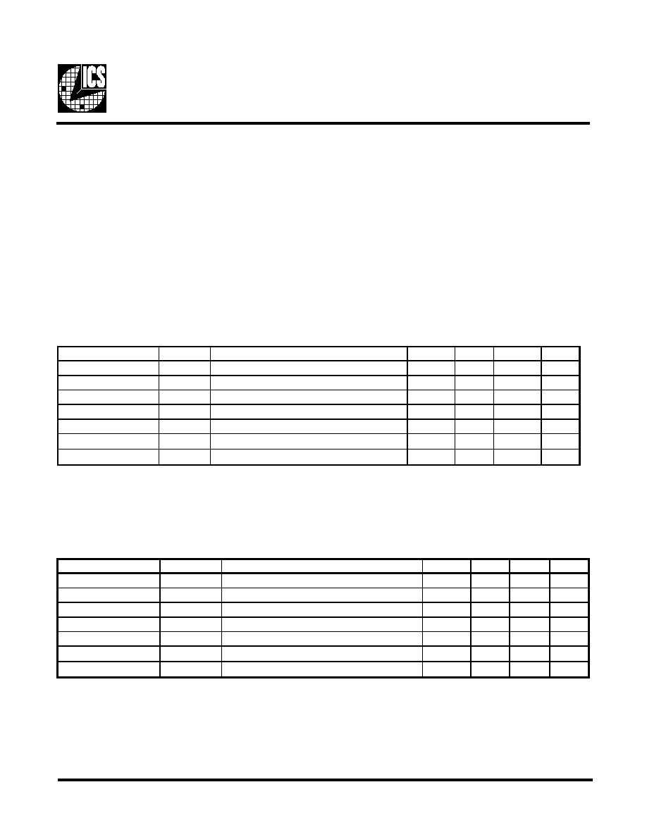
Absolute Maximum Ratings
Supply Voltage . . . . . . . . . . . . . . . . . . . . . . . . . . 7.0 V
Logic Inputs . . . . . . . . . . . . . . . . . . . . . . . . . . . . GND 0.5 V to V
DD
+0.5 V
Ambient Operating Temperature . . . . . . . . . . . . 0°C to +70°C
Storage Temperature . . . . . . . . . . . . . . . . . . . . . . 65°C to +150°C
Stresses above those listed under Absolute Maximum Ratings may cause permanent damage to the device. These ratings are
stress specifications only and functional operation of the device at these or any other conditions above those listed in the
operational sections of the specifications is not implied. Exposure to absolute maximum rating conditions for extended
periods may affect product reliability.
Electrical Characteristics - Input & Supply
T
A
= 0 - 70C; Supply Voltage V
DD
= 5.0 V +/-10% (unless otherwise stated)
PARAMETER
SYMBOL
CONDITIONS
MIN
TYP
MAX
UNITS
Input High Voltage
V
IH
2.0
2.5
VDD +0.5
V
Input Low Voltage
V
IL
GND -0.5
0.8
V
Input High Current
I
IH
V
IN
= V
DD
0.1
100
uA
Input Low Current
I
IL
V
IN
= 0 V;
19
50
uA
Operating current
I
DD1
C
L
= 0 pF; F
IN
@ 66M
45
65
mA
Input frequency
F
i
1
V
DD
= 3.3 V; All Outputs Loaded
25
133
MHz
Input Capacitance
C
IN
1
Logic Inputs
5
pF
1
Guaranteed by design, not 100% tested in production.
Electrical Characteristics - Input & Supply
T
A
= 0 - 70C; Supply Voltage V
DD
= 3.3 V +/-10% (unless otherwise stated)
PARAMETER
SYMBOL
CONDITIONS
MIN
TYP
MAX
UNITS
Input High Voltage
V
IH
2.0
2.0
V
DD
+0.3
V
Input Low Voltage
V
IL
GND-0.3
0.8
V
Input High Current
I
IH
V
IN
= V
DD
0.1
100
uA
Input Low Current
I
IL
V
IN
= 0 V;
19
50
uA
Operating current
I
DD1
C
L
= 0 pF; F
IN
@ 66M
30
45
mA
Input frequency
F
i
1
V
DD
= 3.3 V; All Outputs Loaded
25
133
M Hz
Input Capacitance
C
IN
1
Logic Inputs
5.0
pF
1
Guarenteed by design, not 100% tested in production.
4
ICS9112-17
Electrical Characteristics - OUTPUT
T
A
= 0 - 70C; V
DD
= V
DDL
= 3.3 V +/-10%; C
L
= 20 - 30 pF (unless otherwise stated)
PARAMETER
SYMBOL
CONDITIONS
MIN
TYP
MAX UNITS
Output Impedance
R
DSP
V
O
= V
DD
*(0.5)
10
24
Output Impedance
R
DSN
V
O
= V
DD
*(0.5)
10
24
Output High Voltage
V
OH
I
OH
= -8 mA
2.4
2.9
5.0
V
Output Low Voltage
V
OL
I
OL
= 8 mA
0.25
0.4
V
Rise Time
1
T
r
V
OL
= 0.8 V, V
OH
= 2.0 V
1.2
2.0
ns
Fall Time
1
T
f
V
OH
= 2.0 V, V
OL
= 0.8 V
1.2
2.0
ns
PLL Lock Time1
tLOCK
Stable power supply, valid clock presented on
REF pin
1.0
ms
D
t
V
T
= 1.4V;Cl=30pF
40
50
60
%
D
t
V
T
= Vdd/2; Fout <66.6MHz
45
50
55
%
Tcyc-cyc
at 66MHz , Loaded Outputs
250
ps
Tcyc-cyc
>66MHz , Loaded Outputs
200
ps
Absolute Jitter
1
Tjabs
10000 cycles; Cl=30pF
-100
70
100
ps
Jitter; 1-Sigma
1
Tj1s
10000 cycles; Cl=30pF
14
30
ps
Skew
1
T
sk
V
T
= 1.4 V (Window) Output to Output
250
ps
Device to Device Skew
1
Tdsk-Tdsk
Measured at VDD/2 on the CLKOUT
pins of devices
0
700
ps
Delay Input-Output
1
D
R1
V
T
= 14 V
0
700
ps
1
Guaranteed by design, not 100% tested in production.
Cycle to Cycle jitter
1
Duty Cycle
1
Electrical Characteristics - OUTPUT
T
A
= 0 - 70C; V
DD
= V
DDL
= 5.0 V +/-10%; C
L
= 20 - 30 pF (unless otherwise stated)
PARAMETER
SYMBOL
CONDITIONS
MIN
TYP
MAX UNITS
Output Impedance
R
DSP
V
O
= V
DD
*(0.5)
10
24
Output Impedance
R
DSN
V
O
= V
DD
*(0.5)
10
24
Output High Voltage
V
OH
I
OH
= -8 mA
2.4
2.9
5.0
V
Output Low Voltage
V
OL
I
OL
= 8 mA
0.25
0.4
V
Rise Time
1
T
r
V
OL
= 0.8 V, V
OH
= 2.0 V
0.8
1.5
ns
Fall Time
1
T
f
V
OH
= 2.0 V, V
OL
= 0.8 V
1.0
1.5
ns
PLL Lock Time
1
tLOCK
Stable power supply, valid clock presented on
REF pin
1.0
ms
Duty Cycle
1
D
t
V
T
= 1.4V;Cl=30pF
40
50
60
%
Tcyc-cyc
at 66MHz , Loaded Outputs
250
ps
Tcyc-cyc
>66MHz , Loaded Outputs
200
ps
Absolute Jitter
1
Tjabs
10000 cycles; Cl=30pF
-100
60
100
ps
Jitter; 1-Sigma
1
Tj1s
10000 cycles; Cl=30pF
14
30
ps
Skew
1
T
sk
V
T
= 1.4 V (Window) Output to Output
250
ps
Device to Device Skew
1
Tdsk-Tdsk
Measured at VDD/2 on the CLKOUT
pins of devices
0
700
ps
Delay Input-Output
1
D
R1
V
T
= 14 V
0
700
ps
1
Guaranteed by design, not 100% tested in production.
Cycle to Cycle jitter
1
5
ICS9112-17
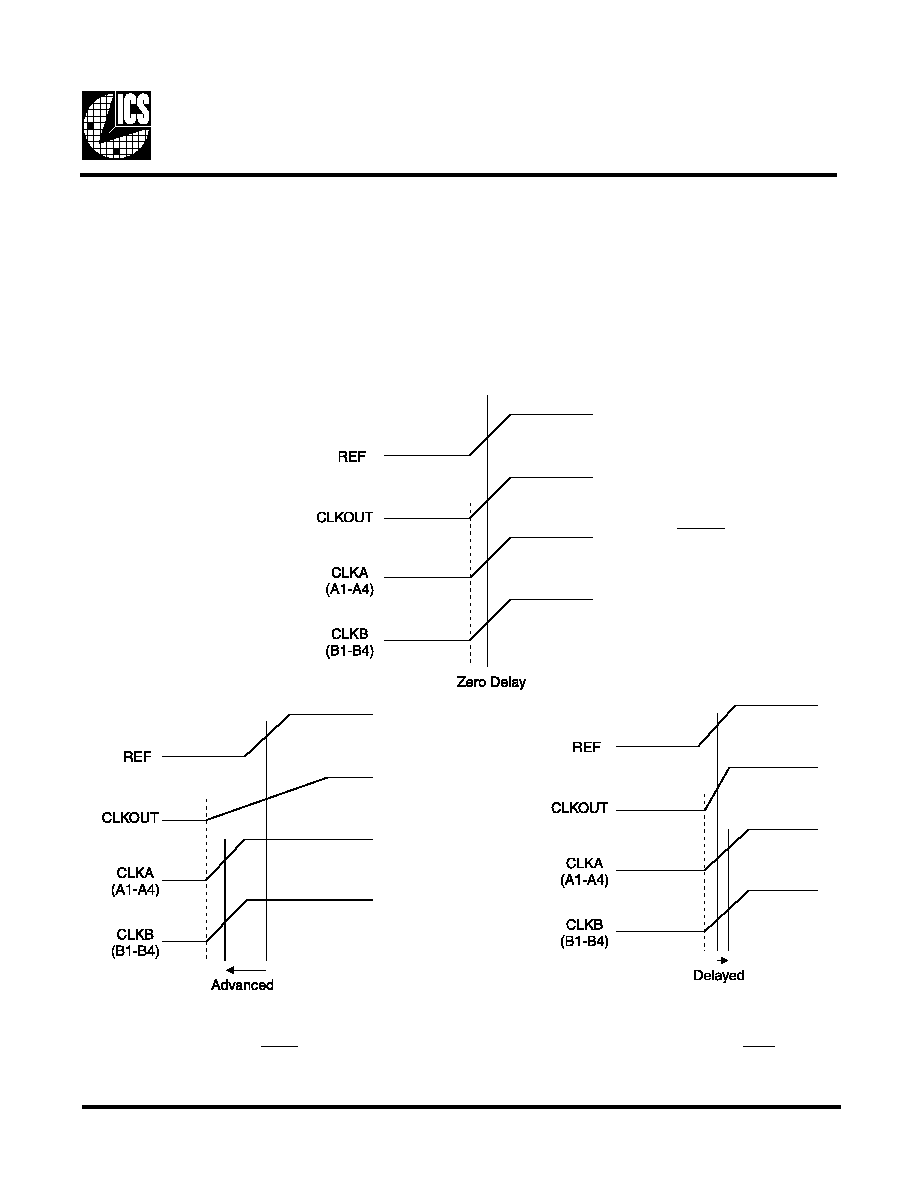
Output to Output Skew
The skew between CLKOUT and the CLKA/B outputs is not dynamically adjusted by the PLL. Since CLKOUT is one of the
inputs to the PLL, zero phase difference is maintained from REF to CLKOUT. If all outputs are equally loaded, zero phase
difference will maintained from REF to all outputs.
If applications requiring zero output-output skew, all the outputs must equally loaded.
If the CLKA/B outputs are less loaded than CLKOUT, CLKA/B outputs will lead it; and if the CLKA/B is more loaded than
CLKOUT, CLKA/B will lag the CLKOUT.
Since the CLKOUT and the CLKA/B outputs are identical, they all start at the same time, but different loads cause them to
have different rise times and different times crossing the measurement thresholds.
REF input and
all outputs
loaded Equally
REF input and CLKA/B
outputs loaded equally, with
CLKOUT loaded More.
REF input and CLKA/B
outputs loaded equally, with
CLKOUT loaded Less.
Timing diagrams with different loading configurations