Integrated
Circuit
Systems, Inc.
General Description
Features
ICS9120-56
Frequency Timing Generator for EtherNet & Hard Drives
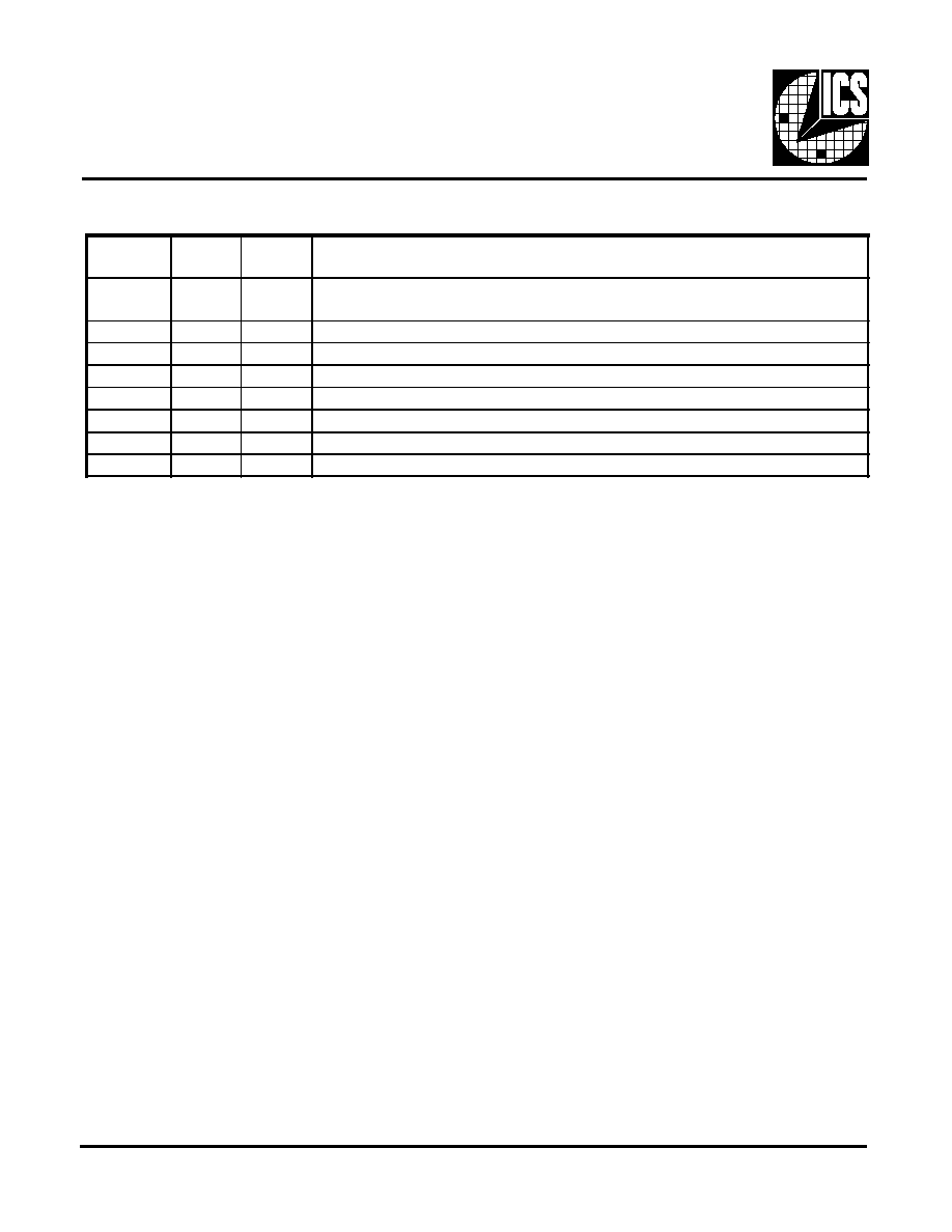
Block Diagram
∑
Single 25.00 MHz crystal or system clock reference
∑
100ps one sigma jitter maintains 16-bit performance
∑
Output rise/fall times less than 2.0ns
∑
On-chip loop filter components
∑
3.3V-5V supply range
∑
8-pin, 150-mil SOIC
Applications
∑
Specifically designed to support the high performance
requirements of high speed EtherNet systems using
10Base-T/100Base-TX Integrataed PHYceiver.
∑
Designed to support the requirements for high
performance hard drives.
The ICS9120-56 is a high performance frequency generator
designed to support hard disk drive and EtherNet systems. It
offers all clock frequencies required for the servo and decoder
sections of these devices. These frequencies are synthesized
from a single 25.00 MHz on-chip oscillator.
High accuracy, low jitter PLLs meet the 100 ppm frequency
tolerance required by these systems. Fast output clock
edge rates minimize board induced jitter.
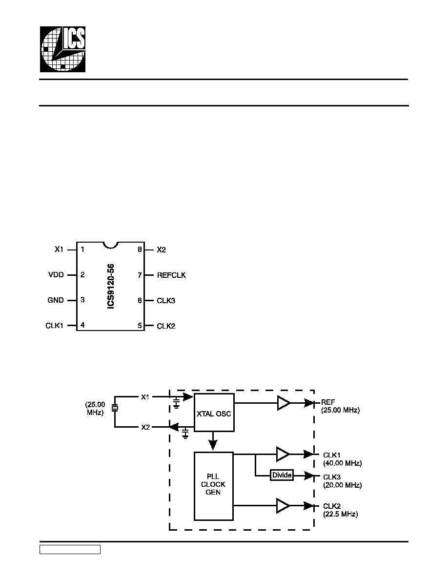
Pin Configuration
8-Pin SOIC
9120-56 Rev A 040697P
2
ICS9120-56
Pin Descriptions for ICS9120-56
PIN
NUMBER
PIN
NAME
TYPE
DESCRIPTION
1
X1
Input
Crystal or external clock source. Has feedback bias for crystal, and internal
crystal load capacitors to GND.
2
VDD
Power
+Power supply input.
3
GND
Power
Ground return for Pin 2.
4
CLK1
Output
40.00 M Hz clock output.
5
CLK2
Output
22.5 MHz output clock.
6
CLK3
Output
20.00 M Hz output clock.
7
REF
Output
Reference clock
8
X2
Output
Crystal output drive, includes internal crystal load capacitor to GND.

3
ICS9120-56
Electrical Characteristics at 3.3 V
V
DD
= +3.0 to +3.7 V, T
A
= 0
O
C-70
o
C unless otherwise stated
1: Parameter is guaranteed by design and characterization. Not 100% tested in production.
2: For direct drive of X1 input.
3. 1ms Ramp @ 1.4V to 1
st
crossing.
Absolute Maximum Ratings
Supply Voltage .......................................................................................................... 7.0 V
Logic Inputs ....................................................................... GND ≠0.5 V to V
DD
+0.5 V
Ambient Operating Temperature ............................................................. 0∞C to +70∞C
Storage Temperature ........................................................................... ≠65∞C to +150∞C
Stresses above those listed under Absolute Maximum Ratings may cause permanent damage to the device. These ratings
are stress specifications only and functional operation of the device at these or any other conditions above those listed
in the operational sections of the specifications is not implied. Exposure to absolute maximum rating conditions for
extended periods may affect product reliability.
DC Characteristics
PARAMETER
SYMBOL
TEST CONDITIONS
MIN
TYP
MAX
UNITS
Input Low Voltage
1
, X1
2
V
IL
0.8
V
Input High Voltage
1
, X1
2
V
IH
2.0
V
Output Low Voltage
V
OL
I
OL
=6.0mA
0.05V
DD
0.1V
DD
V
Output High Voltage
V
OH
I
OH
=4.0mA
0.85V
DD
0.94V
DD
V
Output Low Current
I
OL
V
OL
=0.2V
DD
15.0
24
mA
Output High Current
I
OH
V
OH
=0.7V
DD
-13
-8.0
mA
Supply Current
I
DD
Unloaded V
DD
5.5V
16
30.0
mA
AC Characteristics
Rise Time
1
T
r
15pF load 0.8 to 2.0V
2.3
ns
Fall Time
1
T
f
15pF load 2.0 to 0.8V
0.8
1.5
ns
Duty Cycle
1
D
t
15pF load @ 1.5V V
DD
Except REFCLK
45
50
55
%
Duty Cycle
1
D
t
15pF load @ 1.5V V
DD
Except REFCLK
55
6
65
%
Jitter, One Sigma
1
T
jis
For all frequencies except
REFCLK
120
200
ps
Jitter Absolute
1
T
jab
For all frequencies except
REFCLK
-500
310
500
ps
Jitter, One Sigma
1
T
jis
REFCLK only
0.9
3
%
Jitter Absolute
1
T
jab
REFCLK only
1.9
4
%
Input Frequency
1
F
I
1
30
MHz
Output Frequency Range
1
F
o
1.6
48
MHz
Output Mean Frequency
1
Accuracy vs. Target
F
oa
With 25.00MHz input
-100
0
100
ppm
Power-up Time
1,3
T
pu
0 to 40.0 MHz/1ms Ramp.
7
10
ms
Crystal Input Capacitance
1
C
inx
X1 (Pin 1),
X2 (Pin 8)
16
pF
4
ICS9120-56
Electrical Characteristics at 5.0 V
V
DD
= +4.5 to 5.5 V, T
A
= 0
O
C-70
o
C unless otherwise stated
1: Parameter is guaranteed by design and characterization. Not 100% tested in production.
2: For direct drive of X1 input.
3. 1ms Ramp @ 1.4V to 1
st
crossing.
DC Characteristics
PARAMETER
SYMBOL
TEST CONDITIONS
MIN
TYP
MAX
UNITS
Input Low Voltage
1
, X1
2
V
IL
0.8
V
Input High Voltage
1
, X1
2
V
IH
2.0
V
Output Low Voltage
V
OL
I
OL
=10mA
0.15
0.4
V
Output High Voltage
V
OH
I
OH
=-30mA
2.4
3.7
V
Output Low Current
I
OL
V
OL
=0.8
25
45
mA
Output High Current
I
OH
V
OH
=2.4
-53
-35
mA
Supply Current
I
DD
Unloaded V
DD
5.5V
25
50
mA
AC Characteristics
Rise Time
1
T
r
15pF load 0.8 to 2.0V
0.7
1.5
ns
Fall Time
1
T
f
15pF load 2.0 to 0.8V
0.5
1.5
ns
Rise Time
1
T
r
15pF load 20% to 80%
2.0
4.0
Fall Time
1
T
f
15pF load 80% to 20%
1.4
4.0
Duty Cycle
1
D
t
15pF load @ 1.4V
REFCLK
45
51
55
%
Duty Cycle
1
D
t
15pF load @ 1.4V
REFCLK
55
62
65
%
Jitter, One Sigma
1
T
jis
For all frequencies except
REFCLK
50
100
ps
Jitter Absolute
1
T
jab
For all frequencies except
REFCLK
-400
200
400
ps
Jitter, One Sigma
1
T
jis
REFCLK only
1.2
4
%
Jitter Absolute
1
T
jab
REFCLK only
2.2
5
%
Input Frequency
1
F
I
1
50
MHz
Output Frequency Range
1
F
o
1.6
80
MHz
Output Mean Frequency
1
Accuracy vs. Target
F
oa
With 25.00MHz input
-100
0
100
ppm
Power-up Time
1,3
T
pu
0 to 40.0 MHz;
1ms Ramp.
6
10
ms
Crystal Input Capacitance
1
C
inx
X1 (Pin 1),
X2 (Pin 8)
16
pF
5
ICS9120-56
Ordering Information
ICS9120M-56
0.194
0.031
0.024
0.016
0.050
0.006
± 0.004
0.238
0.154
0.015
0.063
0.025
0.008
8-Pin SOIC Package
Example:
ICS XXXX M-PPP
Package Type
M =SOIC
Device Type (consists of 3 or 4-digit numbers)
Prefix
ICS, AV=Standard Device
Pattern Number (2 or 3-digit number for parts with ROM code pattern)