Integrated
Circuit
Systems, Inc.
General Description
Features
ICS9120-47
Modem and Audio Clock Generator
9120-47 Rev B 071696
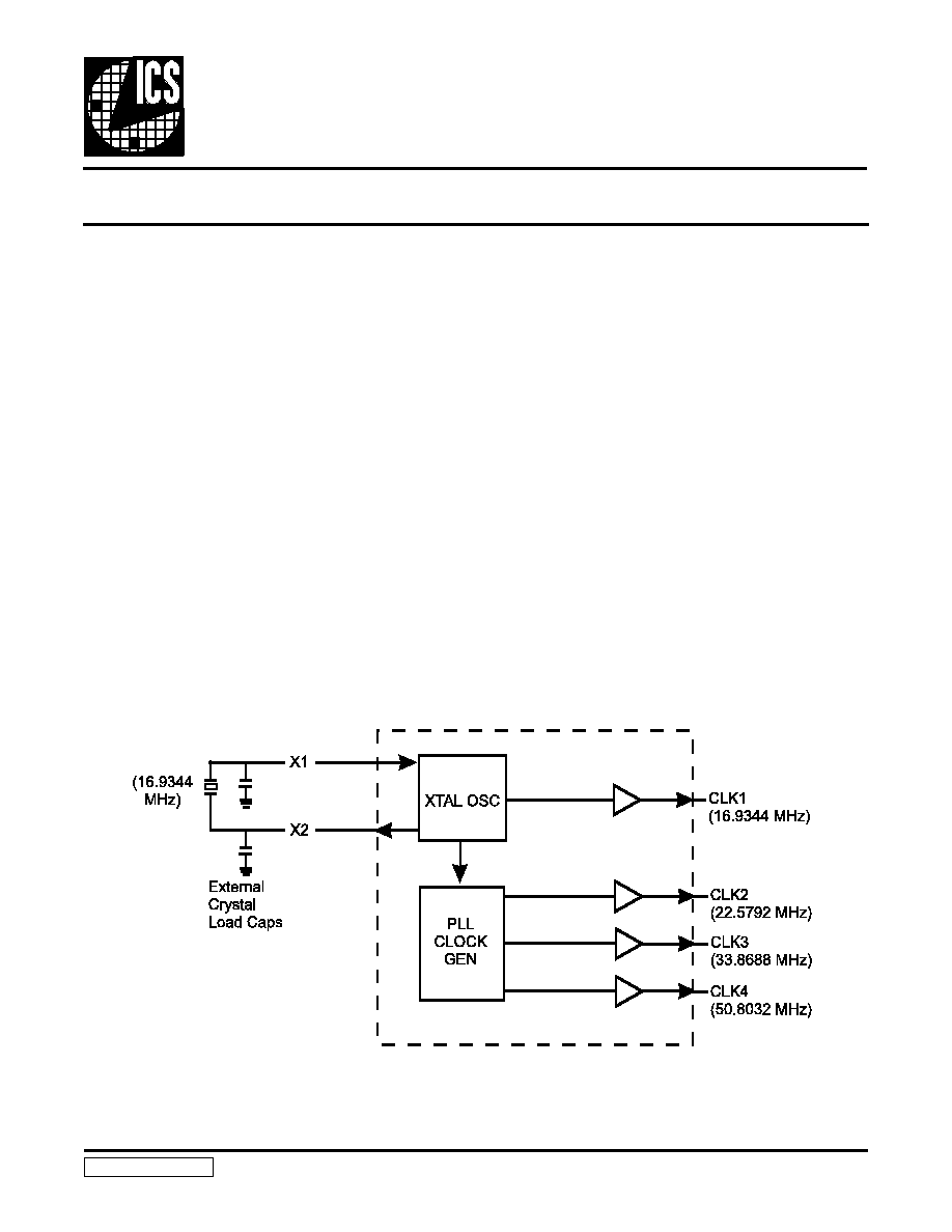
Block Diagram
The ICS9120-47 is a high performance frequency generator
designed to support digital compact disk drive systems. It
offers all clock frequencies required for the servo and decoder
sections of these devices. These frequencies are synthesized
from a single 16.9344 MHz on-chip oscillator.
High accuracy, low jitter PLLs meet the 150 ppm frequency
tolerance required by these systems. Fast output clock edge
rates minimize board induced jitter.
Unlike competitive devices, the ICS9120-47 operates over
the entire 3.0-5.5V range.
∑
Generates the output clock frequencies required by
CD-ROM drive systems
∑
Single 16.9344 MHz crystal or system clock reference
∑
100ps one sigma jitter
∑
Output rise/fall times less than 2.0ns (at 5V VDD)
∑
On-chip loop filter components
∑
3.0V-5.5V supply range
∑
150 ppm output frequency accuracy
∑
8-pin, 150-mil SOIC
Applications
∑
Specifically designed to support CD-ROM drive
requirements of multimedia applications
2
ICS9120-47
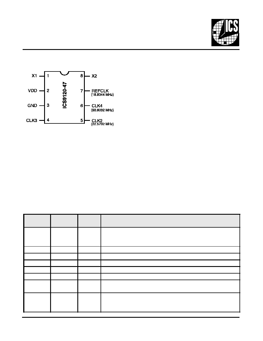
Pin Configuration
Pin Descriptions for ICS9120-47
8-Pin SOIC
External Components/Crystal Selection
The ICS9120-47 incorporates a crystal oscillator circuit de-signed
to provide 50% duty cycle over a range of operating conditions,
including the addition of external crystal load ca-pacitors to pins
X1 and X2.
For the crystal oscillator, the crystal load capacitance must be
connected externally by adding a capacitor from each of the X1
and X2 pins to ground. A parallel resonant 16.9344 MHz crystal is
recommended.
Duty cycle is also maintained when using an external clock source
(connected to X1, X2 left unconnected) as long as the external
clock has good duty cycle.
PIN
NUMBER
PIN NAME
TYPE
DESCRIPTION
1
X1
Input
Crystal or external clock source. Has feedback bias for crystal.
Nominally 16.9344 MHz input applied. (No internal load cap; must
connect external load cap to ground for crystal oscillator).
2
VDD
Power
+Power supply input.
3
GND
Power
Ground return for Pin 2.
4
CLK3
Output
33.8688 MHz target output clock (with nominal 16.9344 MHz input).
5
CLK2
Output
22.5792 MHz target output clock (with nominal 16.9344 MHz input).
6
CLK4
Output
50.8032 MHz target output clock (with nominal 16.9344 MHz input).
7
REFCLK
Output
16.9344 MHz reference clock buffered output (with nominal 16.9344
MHz input).
8
X2
Output
Crystal output drive (leave this pin unconnected when using an
external clock). (No internal load cap; must connect external load cap
to ground for crystal oscillator).
3
ICS9120-47
Absolute Maximum Ratings
Electrical Characteristics at 5 V
V
DD
= +4.5 to +5.5 V, T
A
= 0 to 70
o
C unless otherwise stated
*Parameter is guaranteed by design and characterization. Not 100% tested in production.
AVDD, VDD referenced to GND .......................................................................... 7V
Operating temperature under bias .................................................... 0
o
C to +70
o
C
Storage temperature ..................................................................... -65
o
C to +150
o
C
Voltage on I/O pins referenced to GND ...................... GND -0.5V to VDD +0.5V
Power dissipation ...................................................................................... 0.5 Watts
Stresses above those listed under Absolute Maximum Ratings may cause permanent damage to the device. This is a stress
rating only and functional operation of the device at these or any other conditions above those indicated in the operational
sections of the specifications is not implied. Exposure to absolute maximum rating conditions for extended periods may
affect product reliability.
DC Characteristics
PARAMETER
SYMBOL
TEST CONDITIONS
MIN
TYP
MAX
UNITS
Input Low Voltage
V
IL
-
-
0.8
V
Input High Voltage
V
IH
2.0
-
-
V
Input Low Current
I
IL
V
IN
=0V
-18.0
-8.3
-
µA
Input High Current
I
IH
V
IN
=V
DD
-
-
5.0
µA
Output Low Voltage
V
OL
*
IOL=+10mA
-
0.15
0.4
V
Output High Voltage
V
OH
*
IOH=-30mA
2.4
3.7
-
V
Output Low Current
I
OL
*
V
OL
=0.8V
25.0
45.0
-
mA
Output High Current
I
OH
*
V
OH
=2.4V
-
-53.0
-35.0
mA
Supply Current
I
DD
*
Unloaded
-
30.0
70.0
mA
Pull-up Resistor Value
Rpu*
-
400.0
800.0
k ohm
AC Characteristics
Rise Time
Tr*
15pF load 0.8 to 2.0V
-
0.8
2.0
ns
Fall Time
T
f
*
15pF load 2.0 to 0.8V
-
0.6
1.5
ns
Rise Time
T
r
*
15pF load 20% to 80%
-
1.7
2.5
ns
Fall Time
T
f
*
15pF load 80% to 20%
-
1.1
2.0
ns
Duty Cycle
D
t
*
15pF load @ 50% of
VDD; Except REFCLK
45.0
50.0
55.0
%
Duty Cycle
D
t
*
15pF load @ 50% of
VDD; REFCLK only
40.0
55.0
60.0
%
Jitter, One Sigma
T
jis
*
For all frequencies except
REFCLK
-
100.0
140.0
ps
Jitter, Absolute
T
jab
*
For all frequencies
except REFCLK
-400.0
250.0
400.0
ps
Jitter, One Sigma
T
jis
*
REFCLK only
-
150.0
150.0
ps
Jitter Absolute
T
jab
*
REFCLK only
-700.0
400.0
700.0
ns
Input Frequency Range
F
i
*
11.0
14.0
17.0
MHz
Output Frequency Range
F
o
*
14.0
-
52.0
MHz
Power-up Time
T
pu
*
0 to 40.3 MHz
-
5.5
12.0
ms
Crystal Input Capacitance
C
inx
*
X1 (Pin 1),
X2 (Pin 8)
-
5
-
pF
4
ICS9120-47
Electrical Characteristics at 3.3 V
V
DD
= +3.0 to +3.7 V, T
A
= 0
O
C-70
o
C unless otherwise stated
*Parameter is guaranteed by design and characterization. Not 100% tested in production.
DC Characteristics
PARAMETER
SYMBOL
TEST CONDITIONS
MIN
TYP
MAX
UNITS
Input Low Voltage
V
IL
-
-
0.2V
DD
V
Input High Voltage
V
IH
0.7V
DD
-
-
V
Input Low Current
I
IL
V
IN
=0V
-8.0
-3.6
-
µA
Input High Current
I
IH
V
IN
=VDD
-
-
5.0
µA
Output Low Voltage
V
OL
*
I
OL
=6.0mA
-
0.05V
DD
0.1
V
Output High Voltage
V
OH
*
I
OH
=4.0mA
0.85V
DD
0.94V
DD
-
V
Output Low Current
I
OL
*
V
O
L=0.2V
DD
15.0
24.0
-
mA
Output High Current
I
OH
*
V
OH
=0.7V
DD
-
-13.0
-8.0
mA
Supply Current
I
DD
*
Unloaded
-
20.0
45.0
mA
AC Characteristics
Rise Time
Tr*
15pF load 0.8 to 2.0V
-
2.2
3.5
ns
Fall Time
T
f
*
15pF load 2.0 to 0.8V
-
1.2
2.0
ns
Rise Time
T
r
*
15pF load 20% to 80%
-
2.5
3.5
ns
Fall Time
T
f
*
15pF load 80% to 20%
-
1.4
2.5
ns
Duty Cycle
D
t
*
15pF load @ 50% of
VDD; Except REFCLK
45.0
50.0
55.0
%
Duty Cycle
D
t
*
15pF load @ 50% of
VDD; REFCLK only
45.0
57.0
65.0
%
Jitter, One Sigma
T
jis
*
For all frequencies
except REFCLK
-
150.0
200
ps
Jitter Absolute
T
jab
*
For all frequencies
except REFCLK
-500.0
300.0
500.0
ps
Jitter, One Sigma
T
jis
*
REFCLK only
-
170.0
250.0
ps
Jitter, Absolute
T
jab
*
REFCLK only
-500.0
350.0
500.0
ns
Input Frequency Range
F
i
*
11.0
14.3
15.0
MHz
Output Frequency Range
F
o
*
14.0
-
52.0
MHz
Power-up Time
T
pu*
0 to 40.3 MHz
-
5.5
12.0
ms
Crystal Input Capacitance
C
inx*
X1 (Pin 1),
X2 (Pin 8)
-
5
-
pF
5
ICS9120-47
Ordering Information
ICS9120M-47
0.194
0.031
0.024
0.016
0.050
0.006
± 0.004
0.238
0.154
0.015
0.063
0.025
0.008
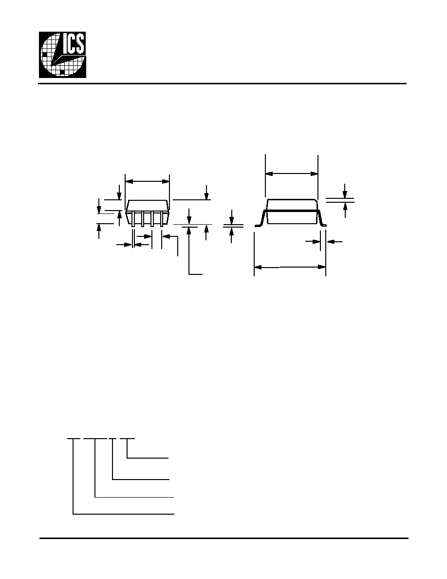
8-Pin SOIC Package
Example:
ICS XXXX M-PPP
Package Type
M =SOIC
Device Type (consists of 3 or 4-digit numbers)
Prefix
ICS, AV=Standard Device
Pattern Number (2 or 3-digit number for parts with ROM code pattern)