Integrated
Circuit
Systems, Inc.
General Description
Features
ICS91309
Preliminary Product Preview
0093E--04/30/03
Block Diagram
High Performance Communication Buffer
Pin Configuration
∑
Zero input - output delay
∑
Frequency range 10 - 133 MHz (3.3V)
∑
5V tolerant input REF
∑
High loop filter bandwidth ideal for Spread Spectrum
applications.
∑
Less than 125 ps cycle to cycle Jitter
∑
Skew controlled outputs
∑
Available in 16 pin, 150 mil SSOP, SOIC & 4.40mm
TSSOP packages
∑
Skew: Group-to-Group: <215 ps
∑
Skew within Group: <100 ps
∑
Industrial temperature range: 0∞C to +70∞C
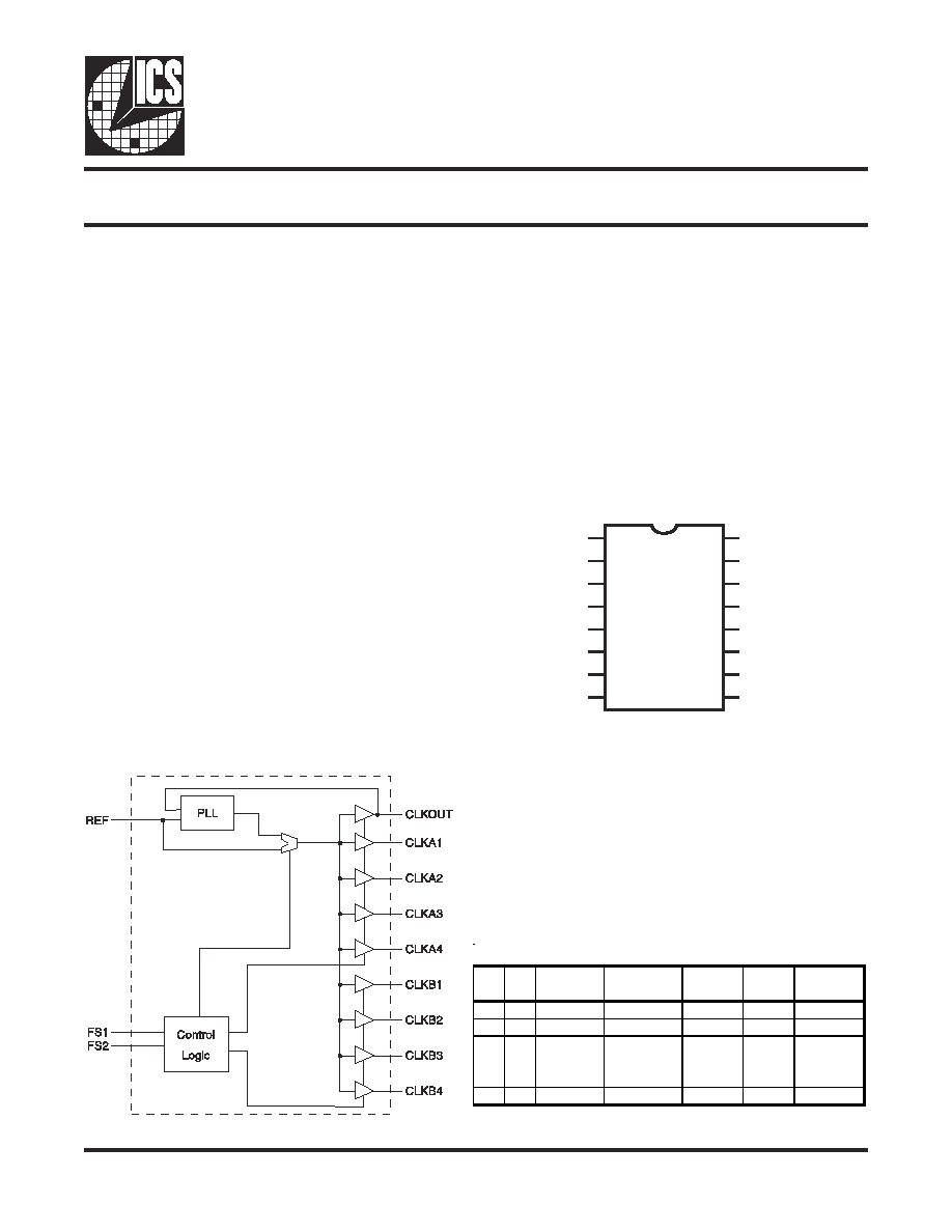
The ICS91309 is a high performance, low skew, low jitter
zero delay buffer. It uses a phase lock loop (PLL)
technology to align, in both phase and frequency, the REF
input with the CLKOUT signal. It is designed to distribute
high speed clocks in communication systems operating
at speeds from 10 to 133 MHz.
The ICS91309 provides synchronization between the
input and output. The synchronization is established via
CLKOUT feed back to the input of the PLL. Since the skew
between the input and output is less than +/- 350 pS, the
part acts as a zero delay buffer.
ICS91309 has two banks of four outputs controlled by two
address lines. Depending on the selected address line,
bank B or both banks can be put in a tri-state mode. In this
mode, the PLL is still running and only the output buffers
are put in a high impedance mode. The test mode shuts
off the PLL and connects the input directly to the output
buffers (see table below for functionality).
ICS91309 comes in a 16-pin 150 mil SOIC, SSOP or
4.40mm TSSOP package. In the absence of REF input,
the device will enter a powerdown mode. In this mode, the
PLL is turned off and the output buffers are pulled low.
Power down mode provides the lowest power consumption
for a standby condition.
16 pin SSOP, SOIC & TSSOP
PRODUCT PREVIEW documents contain information on new products in the sampling or preproduction phase of development. Characteristic data and other specifications are subject to
change without notice.
REF
CLKA1
CLKA2
VDD
GND
CLKB1
CLKB2
FS2
CLKOUT
CLKA4
CLKA3
VDD
GND
CLKB4
CLKB3
FS1
ICS91309
1
2
3
4
5
6
7
8
16
15
14
13
12
11
10
9
Functionality
FS2 FS1 CLKA(1:4) CLKB(1:4) CLKOUT
Ouput
Source
PLL
Shutdown
0
0
Tristate
Tristate
Driven
PLL
N
0
1
Driven
Tristate
Driven
PLL
N
1
0
PLL
Bypass
Mode
PLL Bypass
Mode
PLL
Bypass
Mode
REF
Y
1
1
Driven
Driven
Driven
PLL
N

2
ICS91309
Preliminary Product Preview
0093E--04/30/03
Pin Descriptions
PIN # PIN NAME
PIN TYPE
DESCRIPTION
1
REF
1
IN
Input reference frequency, 5V tolerant input
2
CLKA1
2
OUT
Buffered clock output, Bank A
3
CLKA2
2
OUT
Buffered clock output, Bank A
4, 13 VDD
PWR
Power Supply
5, 12 GND
PWR
Ground
6
CLKB1
2
OUT
Buffered clock output, Bank B
7
CLKB2
2
OUT
Buffered clock output, Bank B
8
FS2
3
IN
Function select input, bit 2
9
FS1
3
IN
Function select input, bit 1
10
CLKB3
2
OUT
Buffered clock output, Bank B
11
CLKB4
2
OUT
Buffered clock output, Bank B
14
CLKA3
2
OUT
Buffered clock output, Bank A
15
CLKA4
2
OUT
Buffered clock output, Bank A
16
CLKOUT
2
OUT
Buffered clock output, internal feedback
Notes:
1. Weak pull-down
2. Weak pull-down on all outputs
3. Weak pull-ups on these inputs

3
ICS91309
Preliminary Product Preview
0093E--04/30/03
Absolute Maximum Ratings
Supply Voltage . . . . . . . . . . . . . . . . . . . . . . . 7.0 V
Logic Inputs (Except REF) . . . . . . . . . . . . . . GND ≠0.5 V to V
DD
+ 0.5 V
Logic Input REF . . . . . . . . . . . . . . . . . . . . . . GND ≠0.5 V to GND + 5.5 V
Ambient Operating Temperature . . . . . . . . . . 0∞C to +70∞C
Storage Temperature . . . . . . . . . . . . . . . . . . . ≠65∞C to +150∞C
Stresses above those listed under
Absolute Maximum Ratings may cause permanent damage to the device. These
ratings are stress specifications only and functional operation of the device at these or any other conditions above those
listed in the operational sections of the specifications is not implied. Exposure to absolute maximum rating conditions
for extended periods may affect product reliability.
Electrical Characteristics - Input & Supply
T
A
= 0 - 70∞C; Supply Voltage V
DD
= 3.3 V +/-10%
PARAMETER
SYMBOL
CONDITIONS
MIN
TYP
MAX
UNITS
Input High Voltage
V
IH
2
V
Input Low Voltage
V
IL
0.8
V
Input High Current
I
IH
V
IN
= V
DD
0.1
100
uA
Input Low Current
I
IL
V
IN
= 0 V
19
50
uA
Output High Voltage
Vo
H
Io
H
= -12 mA
2.4
V
Output Low Voltage
Vo
L
Io
L
= 12 mA
0.4
V
Operating Supply
Current
I
DD
Outputs Unloaded; REF = 66 MHz
30
45
mA
Powerdown Current
I
DD
REF = 0 Mhz
0.3
12
uA
Input Frequency
F
i
10
133
MHz
Input Capacitance
1
C
IN
5
pF
NOTES:
1. Guaranteed by design and characterization, not 100% tested in production.

4
ICS91309
Preliminary Product Preview
0093E--04/30/03
Electrical Characteristics - Outputs
T
A
= 0 - 70∞C; V
DD
= 3.3 V +/-10%; C
L
= 30 pF (unless otherwise specified)
PARAMETER
SYMBOL
CONDITIONS
MIN
TYP
MAX
UNITS
Output High Voltage
V
OH
I
OH
= -12 mA
2.4
V
Output Low Voltage
V
OL
I
OL
= 12 mA
0.4
V
Rise Time
1
t
r
Measure between 0.8 V and 2.0 V
1.2
1.5
ns
Fall Time
1
t
f
Measure between 2.0 V and 0.8 V
1.2
1.5
ns
PLL Lock Time
1
T
LOCK
Stable V
DD
, valid clock on REF
1
mS
f
1
C
L
= 30 pF
10
100
MHz
f
1
C
L
= 10 pF
10
133
MHz
Dt1
Measured at 1.4 V, Fout = 66.7 MHz
40
50
60
%
Dt2
Measured at V
DD
/2, Fout < 50.0 MHz
45
50
55
%
Jitter, Cycle-to-cycle
1
t
jcyc-cyc
Measured at 66.7 MHz, loaded outputs
125
ps
Jitter, Absolute
1
Tjabs
10,000 cycles, C
L
= 30 pF
-100
70
100
ps
Jitter, 1-Sigma
1
Tj1s
10,000 cycles, C
L
= 30 pF
14
30
ps
Skew, Group-to-Group
1
Tsk
Measured at 1.4 V
215
ps
Skew, Output-to-Output
1
Tsk
Measured at 1.4 V, within a group
100
ps
Skew, Device-to-Device
1
Tdsk-Tdsk Measured at V
DD
/2,on CLKOUT pins
700
ps
Delay, Input-to-Output
1
Dr1
Measured at 1.4 V
700
ps
Notes:
1. Guaranteed by design and characterization, not 100% tested in production.
Duty Cycle
1
Output Frequency

5
ICS91309
Preliminary Product Preview
0093E--04/30/03
Output to Output Skew
The skew between CLKOUT and the CLKA/B outputs is not dynamically adjusted by the PLL. Since CLKOUT is one
of the inputs to the PLL, zero phase difference is maintained from REF to CLKOUT. If all outputs are equally loaded,
zero phase difference will maintained from REF to all outputs.
If applications requiring zero output-output skew, all the outputs must equally loaded.
If the CLKA/B outputs are less loaded than CLKOUT, CLKA/B outputs will lead it; and if the CLKA/B is more loaded
than CLKOUT, CLKA/B will lag the CLKOUT.
Since the CLKOUT and the CLKA/B outputs are identical, they all start at the same time, but different loads cause them
to have different rise times and different times crossing the measurement thresholds.
REF input and
all outputs
loaded Equally
REF input and CLKA/B
outputs loaded equally, with
CLKOUT loaded More.
REF input and CLKA/B
outputs loaded equally, with
CLKOUT loaded Less.
Timing diagrams with different loading configurations

6
ICS91309
Preliminary Product Preview
0093E--04/30/03
Application Suggestion:
ICS91309 is a mixed analog/digital product. The analog portion of the PLL is very sensitive to any random noise
generated by charging or discharging of internal or external capacitor on the power supply pins. This type of noise will
cause excess jitter to the outputs of ICS91309. Below is a recommended lay out to alleviate any addition noise. For
additional information on FT. layout, please refer to our AN07. The 0.1 uF capacitors should be connected as close as
possible to power pins (4 & 13). An Isolated power plane with a 2.2 uF capacitor to ground will enhance the power line
stability.
33
33
33
33
10K
0.1µF
VDD
GND
33
33
33
33
33
10K
0.1µF
VDD
GND
1
2
3
4
5
6
7
8
16
15
14
13
12
11
10
9
REF
CLKA1
CLKA2
VDD
GND
CLKB1
CLKB2
FS2
CLKOUT
CLKA4
CLKA3
VDD
GND
CLKB4
CLKB3
FS1

7
ICS91309
Preliminary Product Preview
0093E--04/30/03
MIN
MAX
MIN
MAX
A
1.35
1.75
.053
.069
A1
0.1
0.25
.0040
.010
A2
--
1.50
--
.059
b
0.20
0.30
.008
.012
c
0.18
0.25
.007
.010
D
E
5.80
6.20
.228
.244
E1
3.80
4.00
.150
.157
e
0.635 BASIC
0.025 BASIC
L
0.40
1.27
.016
.050
N
0∞
8∞
0∞
8∞
ZD
SEE VARIATIONS
SEE VARIATIONS
SYMBOL
SEE VARIATIONS
SEE VARIATIONS
In Inches
COMMON DIMENSIONS
In Millimeters
COMMON DIMENSIONS
SEE VARIATIONS
SEE VARIATIONS
VARIATIONS
ZD
ZD
MIN
MAX
(Ref)
MIN
MAX
(Ref)
16
4.80
5.00
0.23
.189
.197
.009
6/1/00
REV B
N
D mm.
D (inch)
JEDEC MO-137
DOC# 10-0032
Ordering Information
ICS91309yF-T
Designation for tape and reel packaging
Package Type
F = SSOP
Revision Designator (will not correlate with datasheet revision)
Device Type (consists of 3 or 4 digit numbers)
Prefix
ICS, AV = Standard Device
Example:
ICS XXXX y F - T

8
ICS91309
Preliminary Product Preview
0093E--04/30/03
150 mil (Narrow Body) SOIC
MIN
MAX
MIN
MAX
A
1.35
1.75
.0532
.0688
A1
0.10
0.25
.0040
.0098
B
0.33
0.51
.013
.020
C
0.19
0.25
.0075
.0098
D
E
3.80
4.0
.1497
.1574
e
H
5.80
6.20
.2284
.2440
h
0.25
0.50
.010
.020
L
0.40
1.27
.016
.050
N
0∞
8∞
0∞
8∞
VARIATIONS
MIN
MAX
MIN
MAX
16
9.80
10.00
.3859
.3937
SYMBOL
SEE VARIATIONS
SEE VARIATIONS
In Millimeters
COMMON DIMENSIONS
In Inches
COMMON DIMENSIONS
SEE VARIATIONS
1.27 BASIC
0.050 BASIC
N
D mm.
D (inch)
SEE VARIATIONS
Ordering Information
ICS91309yM-T
SEATING
PLANE
SEATING
PLANE
A1
B
A
e
.10 (.004)
.10 (.004)
h x 45∞
h x 45∞
L
C
INDEX
AREA
INDEX
AREA
1 2
1 2
N
D
E
H
Designation for tape and reel packaging
Package Type
M = SOIC
Revision Designator (will not correlate with datasheet revision)
Device Type (consists of 3 or 4 digit numbers)
Prefix
ICS, AV = Standard Device
Example:
ICS XXXX y M - T

9
ICS91309
Preliminary Product Preview
0093E--04/30/03
Ordering Information
ICS91309yG-T
MIN
MAX
MIN
MAX
A
--
1.20
--
.047
A1
0.05
0.15
.002
.006
A2
0.80
1.05
.032
.041
b
0.19
0.30
.007
.012
c
0.09
0.20
.0035
.008
D
E
E1
4.30
4.50
.169
.177
e
L
0.45
0.75
.018
.030
N
0∞
8∞
0∞
8∞
aaa
--
0.10
--
.004
VARIATIONS
MIN
MAX
MIN
MAX
16
4.90
5.10
.193
.201
10-0035
4.40 mm. Body, 0.65 mm. Pitch TSSOP
(173 mil) (25.6 mil)
SYMBOL
In Millimeters
In Inches
COMMON DIMENSIONS
COMMON DIMENSIONS
SEE VARIATIONS
SEE VARIATIONS
6.40 BASIC
0.252 BASIC
0.65 BASIC
0.0256 BASIC
SEE VARIATIONS
SEE VARIATIONS
N
D mm.
D (inch)
Reference Doc.: JEDEC Publication 95, MO-153
INDEX
AREA
INDEX
AREA
1 2
1 2
N
D
E1
E
SEATING
PLANE
SEATING
PLANE
A1
A
A2
e
- C -
- C -
b
c
L
aaa
C
Designation for tape and reel packaging
Package Type
G = TSSOP
Revision Designator (will not correlate with datasheet revision)
Device Type (consists of 3 or 4 digit numbers)
Prefix
ICS, AV = Standard Device
Example:
ICS XXXX y G - T