Äîêóìåíòàöèÿ è îïèñàíèÿ www.docs.chipfind.ru
Integrated
Circuit
Systems, Inc.
General Description
Features
ICS9148-08
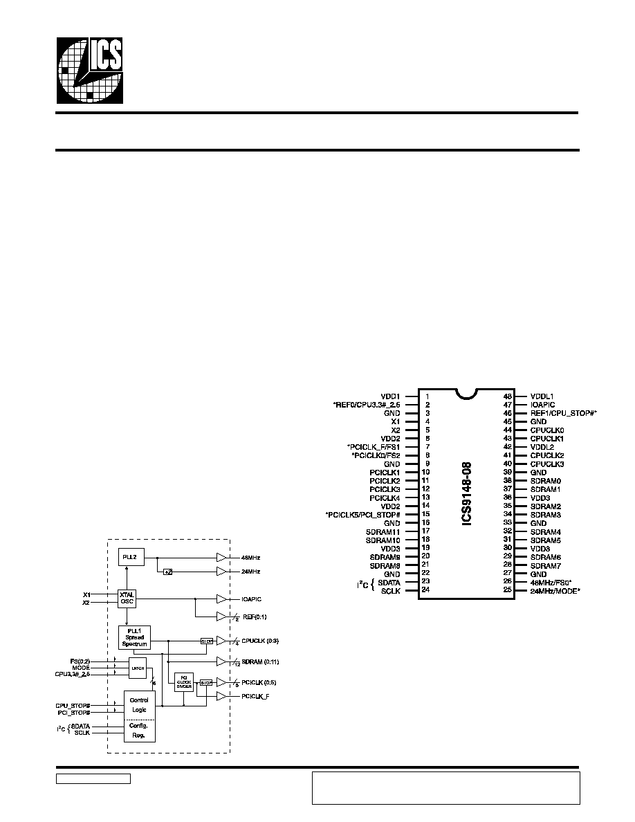
Block Diagram
Frequency Generator & Integrated Buffers for PENTIUM/Pro
TM
9148-08 Rev A 092297P
Pin Configuration
3.3V outputs: SDRAM, PCI, REF, 48/24 MHz
2.5V or 3.3V outputs; CPU, IOAPIC
20 ohm CPU clock output impedance
20 ohm PCI clock output impedance
Skew from CPU (earlier) to PCI clock - 1 to 4 ns,
center 2.6 ns.
No external load cap for C
L
=18pF crystals
±250 ps CPU, PCI clock skew
400ps (cycle to cycle) CPU jitter
Smooth frequency switch , with selections from 50 to 83.3
MHz CPU.
I
2
C interface for programming
2ms power up clock stable time
Clock duty cycle 45-55%.
48 pin 300 mil SSOP package
3.3V operation, 5V tolerant input.
48-Pin SSOP
Power Groups
VDD1 = REF (0:1), X1, X2
VDD2 = PCICLK_F, PCICLK(0:5)
VDD3 = SDRAM (0:11), supply for PLL core,
24MHz, 48MHz
VDDL1 = IOAPIC
VDDL2 = CPUCLK (0:3)
* Internal Pull-up Resistor of
240K to 3.3V on indicated inputs
The ICS9148-08 generates all clocks required for high
speed RISC or CISC microprocessor systems such as Intel
PentiumPro or Cyrix. Eight different reference frequency
multiplying factors are externally selectable with smooth
frequency transitions.
Features include four CPU, seven PCI and Twelve SDRAM
clocks. Two reference outputs are available equal to the
crystal frequency. Plus the IOAPIC output powered by
VDDL1. One 48 MHz for USB, and one 24 MHz clock for
Super IO. Spread Spectrum built in ±1.5% modulation to
reduce the EMI. Serial programming I
2
C interface allows
changing functions, stop clock programing and Frequency
selection. Rise time adjustment for VDD at 3.3V or 2.5V CPU.
Additionally, the device meets the Pentium power-up
stabilization, which requires that CPU and PCI clocks be stable
within 2ms after power-up. It is not recommended to use I/O
dual function pin for the slots (ISA, PCI, CPU, DIMM). The
add on card might have a pull up or pull down.
High drive PCICLK and SDRAM outputs typically provide
greater than 1 V/ns slew rate into 30pF loads. CPUCLK
outputs typically provide better than 1V/ns slew rate into
20pF loads while maintaining 50±5% duty cycle. The REF
and 24 and 48 MHz clock outputs typically provide better
than 0.5V/ns slew rates.
Pentium is a trademark of Intel Corporation
I
2
C is a trademark of Philips Corporation
ICS reserves the right to make changes in the device data identified in this
publication without further notice. ICS advises its customers to obtain the latest
version of all device data to verify that any information being relied upon by the
customer is current and accurate.
2
ICS9148-08
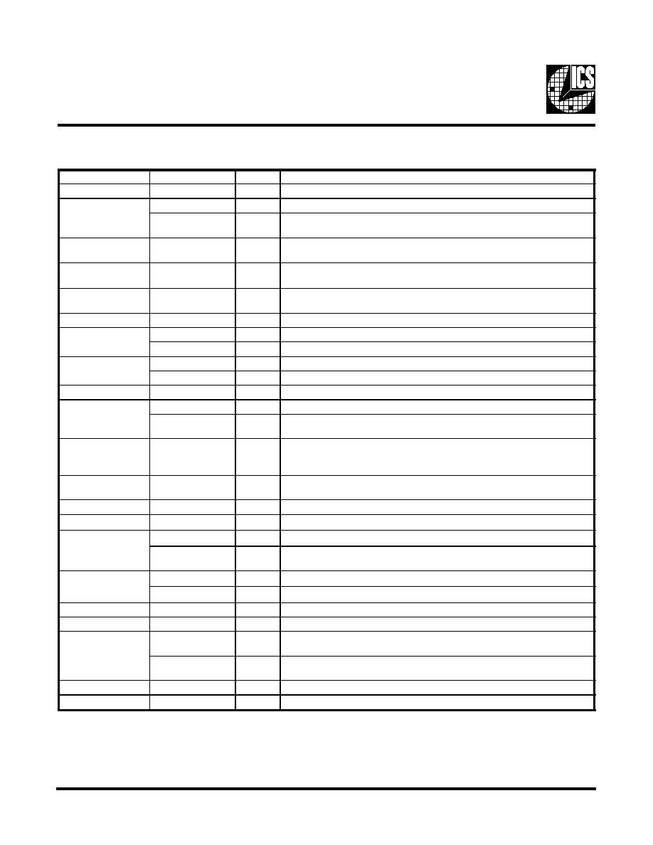
Pin Descriptions
Notes:
1:
Internal Pull-up Resistor of 240K to 3.3V on indicated inputs
2:
Bidirectional input/output pins, input logic levels are latched at internal power-on-reset. Use 10Kohm resistor
to program logic high to VDD or logic low to GND.
PIN NUMBER
PIN NAME
TYPE
DESCRIPTION
1
VDD1
PWR
Ref (0:1), XTAL power supply, nominal 3.3V
2
REF0
OUT
14.318 MHz reference clock.
CPU3.3#_2.5
1 ,2
IN
Indicates whether VDDL2 is 3.3V or 2.5V. High=2.5V CPU,
LOW=3.3V CPU
1
. Latched input
2
3,9,16,22,27,
33,39,45
GND
PWR
Ground
4
X1
IN
Crystal input, has internal load cap (33pF) and feedback
resistor from X2
5
X2
OUT
Crystal output, nominally 14.318MHz. Has internal load
cap (33pF)
6,14
VDD2
PWR
Supply for PCICLK_F and PCICLK (0:5), nominal 3.3V
7
PCICLK_F
OUT
Free running PCI clock
FS1
1 , 2
IN
Frequency select pin. Latched Input
8
PCICLK0
OUT
PCI clock output.
FS2
1 , 2
IN
Frequency select pin. Latched Input
10, 11, 12, 13
PCICLK(1:4)
OUT
PCI clock outputs.
15
PCICLK5
OUT
PCI clock output. (In desktop mode, MODE=1)
PCI_STOP#
1
IN
Halts PCICLK(0:5) clocks at logic 0 level, when input low (In
mobile mode, MODE=0)
17, 18, 20, 21,
28, 29, 31, 32,
34, 35,37,38
SDRAM (0:11)
OUT
SDRAM clock outputs.
19,30,36
VDD3
PWR
Supply for SDRAM (0:11), PLL core and 24,48MHz clocks,
nominal 3.3V
23
SDATA
IN
Data input for
I
2
C serial input.
24
SCLK
IN
Clock input of
I
2
C input
25
24MHz
OUT
24MHz output clock
MODE
1 , 2
IN
Pin 15, pin 46 function select pin, 1=Desktop Mode, 0=Mobile Mode.
Latched Input.
26
48MHz
OUT
48MHz output clock
FS0
1 , 2
IN
Frequency select pin. Latched Input
40, 41, 43, 44
CPUCLK(0:3)
OUT
CPU clock outputs, powered by VDDL2. Low if CPU_STOP#=Low
42
VDDL2
PWR
Supply for CPU (0:3), either 2.5V or 3.3V nominal
46
REF1
OUT
14.318 MHz reference clock, (in Desktop Mode, MODE=1) This
REF output is the STRONGER buffer for ISA BUS loads.
CPU_STOP#
1
IN
Halts CPUCLK (0:3) clocks at logic 0 level, when input low (in
Mobile Mode, MODE=0)
47
IOAPIC
OUT
IOAPIC clock output. 14.318 MHz Powered by VDDL1.
48
VDDL1
PWR
Supply for IOAPIC, either 2.5 or 3.3V nominal
3
ICS9148-08
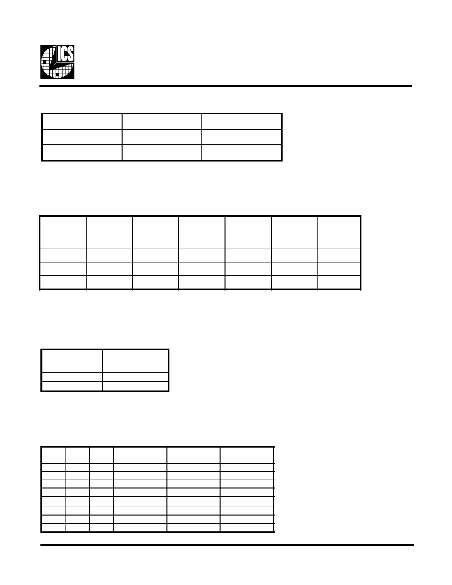
Functionality
V
DD
1,2,3 = 3.3V±5%, V
DDL
1,2 = 2.5V±5% or 3.3±5%, TA=0 to 70°C
Crystal (X1, X2) = 14.31818MHz
CPU3.3#_2.5
Input level
(Latched Data)
Buffer Selected for
operation at:
1
2.5V VDD
0
3.3V VDD
CPU 3.3#_2.5V Buffer selector for CPUCLK and IOAPIC drivers.
Power Management Functionality
FS2
FS1
FS0
CPU,
SDRAM(M Hz)
PCICLK
(MHz)
REF, IOAPIC
(MHz)
0
0
0
50.0
25.0 (1/2 CPU)
14.318
0
0
1
75.0
30 (CPU/2.5)
14.318
0
1
0
83.3
33.3
14.318
0
1
1
68.5
34.25 (1/2 CPU)
14.318
1
0
0
55.0
27.5 (1/2 CPU)
14.318
1
0
1
75.0
37.5 (1/2 CPU)
14.318
1
1
0
60.0
30.0 (1/2 CPU)
14.318
1
1
1
66.8
33.4 (1/2 CPU)
14.318
Mode Pin - Power Management Input Control
MODE, Pin 25
(Latched Input)
Pin 46
Pin 15
0
CPU_STOP#
(INPUT)
PCI_STOP#
(INPUT)
1
REF1
(OUTPUT)
PCICLK5
(OUTPUT)
CPU_STOP#
PCI_STOP#
CPUCLK
Outputs
PCICLK
(0:5)
PCICLK_F,
REF,
24/48MHz
and SDRAM
Crystal
OSC
VCO
0
1
Stopped Low
Running
Running
Running
Running
1
1
Running
Running
Running
Running
Running
1
0
Running
Stopped Low
Running
Running
Running
4
ICS9148-08
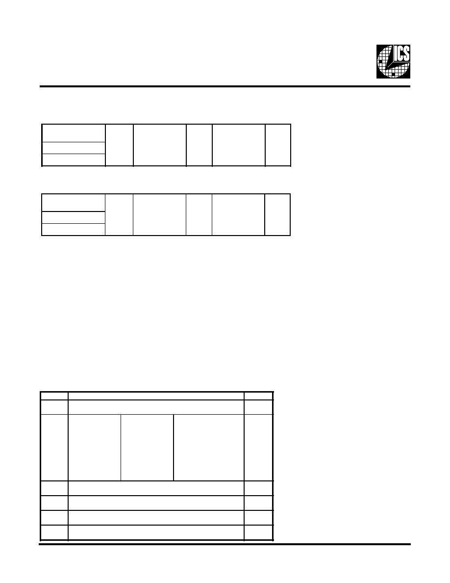
Byte0: Functionality and Frequency Select Register (default = 0)
Serial Configuration Command Bitmap
General I
2
C serial interface information
I
2
C is a trademark of Philips Corporation
A.
For the clock generator to be addressed by an I
2
C controller, the following address must be sent as a start sequence, with
an acknowledge bit between each byte.
B.
The clock generator is a slave/receiver I
2
C component. It can "read back "(in Philips I
2
C protocol) the data stored in the
latches for verification. (set R/W# to 1 above). There is no BYTE count supported, so it does not meet the Intel SMB
PIIX4 protocol.
C.
The data transfer rate supported by this clock generator is 100K bits/sec (standard mode)
D.
The input is operating at 3.3V logic levels.
E.
The data byte format is 8 bit bytes.
F.
To simplify the clock generator I
2
C interface, the protocol is set to use only block writes from the controller. The bytes
must be accessed in sequential order from lowest to highest byte with the ability to stop after any complete byte has
been transferred. The Command code and Byte count shown above must be sent, but the data is ignored for those two
bytes. The data is loaded until a Stop sequence is issued.
G.
In the power down mode (PWR_DWN# Low), the SDATA and SCLK pins are tristated and the internal data latches
maintain all prior programming information.
H.
At power-on, all registers are set to a default condition. See Byte 0 detail for default condition, Bytes 1 through 5 default
to a 1 (Enabled output state)
Then Byte 0, 1, 2, etc in
sequence until STOP.
Byte 0, 1, 2, etc in sequence until STOP.
Clock Generator
Address (7 bits)
ACK
+ 8 bits dummy
command code
ACK
+ 8 bits dummy
Byte count
ACK
A(6:0) & R/W#
D2
(H)
Clock Generator
Address (7 bits)
ACK
Byte 0
ACK
Byte 1
ACK
A(6:0) & R/W#
D3
(H)
Note 1. Default at Power-up will be for
latched logic inputs to define
frequency. Bits 4, 5, 6 are default to
000, and if bit 3 is written to a 1 to
use Bits 6:4, then these should be
defined to desired frequency at same
write cycle.
Note: PWD = Power-Up Default
Bit
Description
PWD
Bit 7
0 - ±1.5% Spread Spectrum Modulation
1 - ±0.6% Spread Spectrum Modulation
0
Bit 6:4
Bit6 Bit5 Bit4
111
110
101
100
011
010
001
000
CPU clock
66.8
60.0
75.0
55.0
68.5
83.3
75.0
50.0
PCI
33.4(1/2 CPU)
30.0 (1/2 CPU)
37.5 (1/2 CPU)
27.5 (1/2 CPU)
34.5 (1/2 CPU)
33.3
30.0 (CPU/2.5)
25.0 (1/2 CPU)
Note1
Bit 3
0 - Frequency is selected by hardware select, Latched Inputs
1 - Frequency is selected by Bit 6:4 (above)
0
0 - Spread Spectrum center spread type.
1 - Spread Spectrum down spread type.
0
Bit 1
0 - Normal
1 - Spread Spectrum Enabled
0
Bit 0
0 - Running
1- Tristate all outputs
0
5
ICS9148-08
Byte 1: CPU, Active/Inactive Register
(1 = enable, 0 = disable)
Byte 2: PCI Active/Inactive Register (1 = enable, 0 = disable)
Byte 3: SDRAM Active/Inactive Register
(1 = enable, 0 = disable)
Notes:
1. Inactive means outputs are held LOW and are disabled
from switching.
Notes:
1. Inactive means outputs are held LOW and are disabled
from switching.
2. PCICLK5 only in Desktop Mode
Notes:
1. Inactive means outputs are held LOW and are disabled
from switching.
Bit
Pin #
PWD
Description
Bit 7
-
1
(Reserved)
Bit 6
-
1
(Reserved)
Bit 5
-
1
(Reserved)
Bit 4
-
1
(Reserved)
Bit 3
40
1
CPUCLK3 (Act/Inact)
Bit 2
41
1
CPUCLK2 (Act/Inact)
Bit 1
43
1
CPUCLK1 (Act/Inact)
Bit 0
44
1
CPUCLK0 (Act/Inact)
Bit
Pin #
PWD
Description
Bit 7
-
1
(Reserved)
Bit 6
7
1
PCICLK_F (Act/Inact)
Bit 5
15
1
PCICLK5 (Act/Inact)
(Desktop only)
Bit 4
14
1
PCICLK4 (Act/Inact)
Bit 3
12
1
PCICLK3 (Act/Inact)
Bit 2
11
1
PCICLK2 (Act/Inact)
Bit 1
10
1
PCICLK1 (Act/Inact)
Bit 0
8
1
PCICLK0 (Act/Inact)
Bit
Pin #
PWD
Description
Bit 7
28
1
SDRAM7 (Act/Inact)
Bit 6
29
1
SDRAM6 (Act/Inact)
Bit 5
31
1
SDRAM5 (Act/Inact)
Bit 4
32
1
SDRAM4 (Act/Inact)
Bit 3
34
1
SDRAM3 (Act/Inact)
Bit 2
35
1
SDRAM2 (Act/Inact)
Bit 1
37
1
SDRAM1 (Act/Inact)
Bit 0
38
1
SDRAM0 (Act/Inact)
Byte 4: SDRAM Active/Inactive Register
(1 = enable, 0 = disable)
Notes:
1. Inactive means outputs are held LOW and are disabled
from switching. These outputs are designed to be
configured at power-on and are not expected to be
configured during the normal modes of operation.
Bit
Pin #
PWD
Description
Bit 7
-
1
(Reserved)
Bit 6
-
1
(Reserved)
Bit 5
-
1
(Reserved)
Bit 4
-
1
(Reserved)
Bit 3
17
1
SDRAM11 (Act/Inact)
Bit 2
18
1
SDRAM10 (Act/Inact)
Bit 1
20
1
SDRAM9 (Act/Inact)
Bit 0
21
1
SDRAM8 (Act/Inact)
Byte 5: Peripheral Active/Inactive Register
(1 = enable, 0 = disable)
Notes:
1. Inactive means outputs are held LOW and are disabled from
switching. These outputs are designed to be configured at
power-on and are not expected to be configured during the
normal modes of operation.
2. REF1 only in Desktop Mode
Bit
Pin #
PWD
Description
Bit 7
-
1
(Reserved)
Bit 6
-
1
(Reserved)
Bit 5
-
1
(Reserved)
Bit 4
47
1
IOAPIC0 (Act/Inact)
Bit 3
-
1
(Reserved)
Bit 2
-
1
(Reserved)
Bit 1
46
1
REF1 (Act/Inact)
Bit 0
2
1
REF0 (Act/Inact)
Bit
Pin #
PWD
Description
Bit 7
-
1
(Reserved)
Bit 6
-
1
(Reserved)
Bit 5
-
1
(Reserved)
Bit 4
-
1
(Reserved)
Bit 3
-
1
(Reserved)
Bit 2
-
1
(Reserved)
Bit 1
-
1
(Reserved)
Bit 0
-
1
(Reserved)
Note: PWD = Power-Up Default
Byte 6: Optional Register For Possible Future Requirements
Notes:
1. Byte 6 is reserved by Integrated Circuit Systems for
future applications.