9148-02
Integrated
Circuit
Systems, Inc.
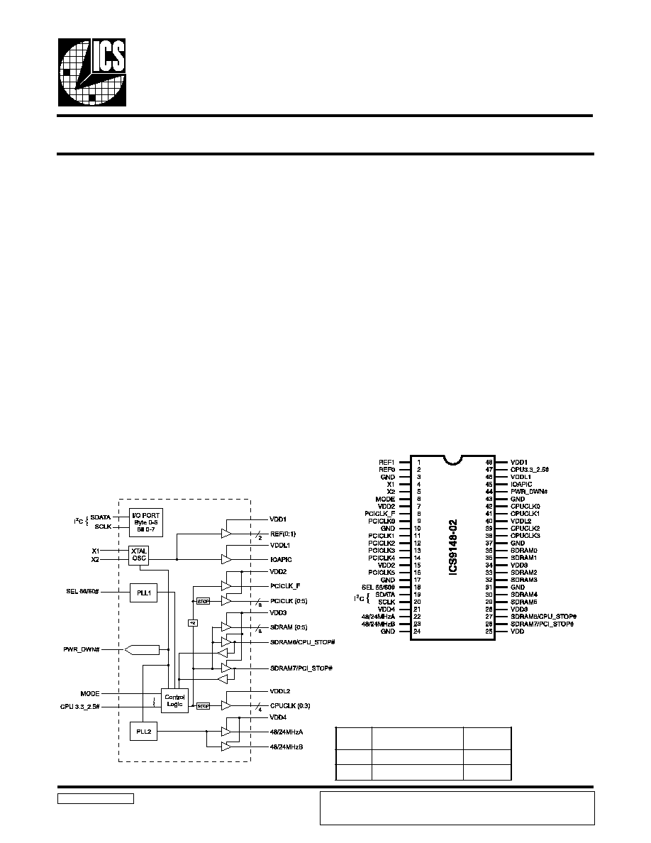
General Description
Features
ICS9148-02
Block Diagram
Pentium/Pro
TM
System Clock Chip
9148-02 Rev C 1/26/99
Pentium is a trademark on Intel Corporation.
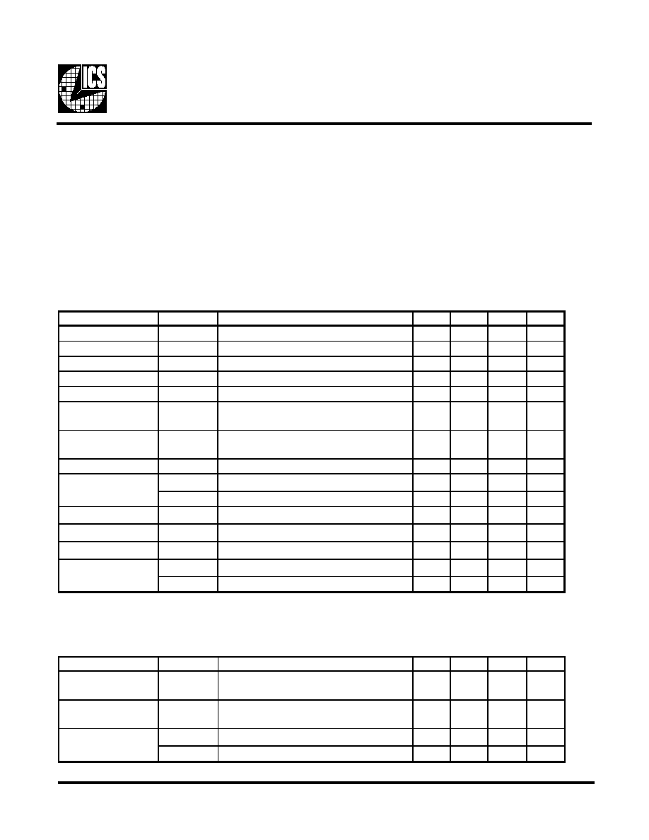
Generates system clocks for CPU, IOAPIC, SDRAM,
PCI, plus 14.314 MHz REF(0:1), USB, Plus Super I/O
Supports single or dual processor systems
I
2
C serial configuration interface provides output clock
disabling and other functions
MODE input pin selects optional power management
input control pins
Two fixed outputs separately selectable as
24 or 48MHz
Separate 2.5V and 3.3V supply pins
2.5V or 3.3V outputs: CPU, IOAPIC
3.3V outputs: SDRAM, PCI, REF, 48/24 MHz
CPU 3.3_2.5# logic pin to adjust output strength
No power supply sequence requirements
Uses external 14.318MHz crystal
48 pin 300 mil SSOP
Output enable register
for serial port control:
1 = enable
0 = disable
The ICS9148-02 is a Clock Synthesizer chip for Pentium and
PentiumPro CPU based Desktop/Notebook systems that will
provide all necessary clock timing.
Features include four CPU, seven PCI and eight SDRAM
clocks. Two reference outputs are available equal to the
crystal frequency. Additionally, the device meets the Pentium
power-up stabilization, which requires that CPU and PCI
clocks be stable within 2ms after power-up.
PWR_DWN# pin allows low power mode by stopping crystal
OSC and PLL stages. For optional power management,
CPU_STOP# can stop CPU (0:3) clocks and PCI_STOP#
will stop PCICLK (0:5) clocks. CPU and IOAPIC output
buffer strength controlled by CPU 3.3_2.5# pin to match
VDDL voltage.
High drive CPUCLK outputs typically provide greater than 1
V/ns slew rate into 20pF loads. PCICLK outputs typically
provide better than 1V/ns slew rate into 30pF loads while
maintaining 50±5% duty cycle. The REF clock outputs typically
provide better than 0.5V/ns slew rates.
The ICS9148-02 accepts a 14.318MHz reference crystal or
clock as its input and runs on a 3.3V core supply.
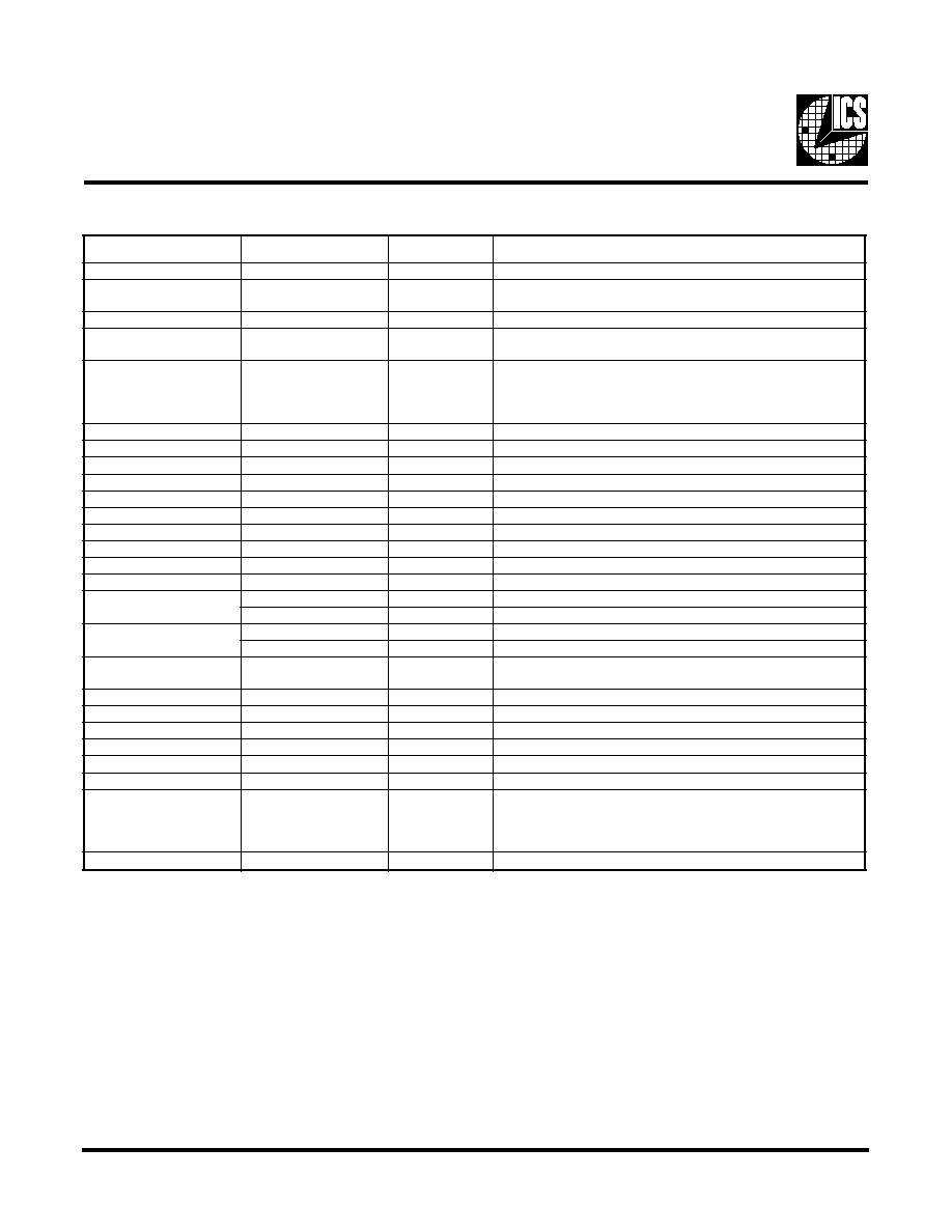
Functionality
VDD (1:4) 3.3V±10%, VDDL1, 2 2.5±5% or 3.3±10% 0-70
°
C
Crystal (X1, X2) = 14.31818 MHz
L
E
S
M
A
R
D
S
,
K
L
C
U
P
C
)
z
H
M
(
K
L
C
I
C
P
)
z
H
M
(
0
0
6
0
3
1
6
.
6
6
3
.
3
3
Pin Configuration
48-Pin SSOP
ICS reserves the right to make changes in the device data identified in this
publication without further notice. ICS advises its customers to obtain the latest
version of all device data to verify that any information being relied upon by the
customer is current and accurate.
2
ICS9148-02
Pin Descriptions
Power Groups
VDD = Supply for PLL core
VDD1 = REF (0:1), X1, X2
VDD2 = PCICLK_F, PCICLK (0:5)
VDD3 = SDRAM (0:5), SDRAM6/CPU_STOP#, SDRAM7/PCI_STOP#
VDD4 = 48/24MHzA, 48/24MHzB
VDDL1 = IOAPIC
VDDL2 = CPUCLK (0:3)
R
E
B
M
U
N
N
I
P
E
M
A
N
N
I
P
E
P
Y
T
N
O
I
T
P
I
R
C
S
E
D
1
,
2
)
1
:
0
(
F
E
R
T
U
O
t
u
p
t
u
O
k
c
o
l
c
e
c
n
e
r
e
f
e
R
,
4
2
,
7
1
,
0
1
,
3
3
4
,
7
3
,
1
3
D
N
G
R
W
P
)
n
o
m
m
o
c
(
d
n
u
o
r
G
4
1
X
N
I
p
a
c
d
a
o
l
l
a
t
s
y
r
c
l
a
n
r
e
t
n
i
s
a
h
,
t
u
p
n
i
e
c
n
e
r
e
f
e
r
r
o
l
a
t
s
y
r
C
5
2
X
T
U
O
k
c
a
b
d
e
e
f
d
n
a
p
a
c
d
a
o
l
l
a
n
r
e
t
n
i
s
a
h
,
t
u
p
t
u
o
l
a
t
s
y
r
C
1
X
o
t
r
o
t
s
i
s
e
r
6
E
D
O
M
N
I
7
2
&
6
2
s
n
i
p
n
e
h
t
,
H
G
I
H
s
i
e
d
o
M
f
I
.
n
o
i
t
c
e
l
e
s
n
o
i
t
c
n
u
f
t
u
p
n
I
e
d
o
M
f
I
.
)
6
M
A
R
D
S
d
n
a
7
M
A
R
D
S
(
s
t
u
p
t
u
o
s
a
d
e
r
u
g
i
f
n
o
c
e
r
a
s
t
u
p
n
i
s
a
d
e
r
u
g
i
f
n
o
c
e
r
a
7
2
&
6
2
s
n
i
p
,
n
e
h
t
,
W
O
L
s
i
.
)
#
P
O
T
S
_
U
P
C
d
n
a
#
P
O
T
S
_
I
C
P
(
5
1
,
7
2
D
D
V
R
W
P
V
3
.
3
l
a
n
i
m
o
n
,
)
5
:
0
(
K
L
C
I
C
P
,
F
_
K
L
C
I
C
P
r
o
f
y
l
p
p
u
S
8
F
_
K
L
C
I
C
P
T
U
O
#
P
O
T
S
_
I
C
P
y
b
d
e
t
c
e
f
f
a
t
o
n
,
k
c
o
l
c
I
C
P
g
n
i
n
n
u
r
e
e
r
F
6
1
,
4
1
,
3
1
,
2
1
,
1
1
,
9
)
5
:
0
(
K
L
C
I
C
P
T
U
O
s
k
c
o
l
c
I
C
P
8
1
#
0
6
/
6
6
L
E
S
N
I
U
P
C
d
n
a
M
A
R
D
S
r
o
f
z
H
M
6
.
6
6
r
o
z
H
M
0
6
s
t
c
e
l
e
S
9
1
A
T
A
D
S
N
I
I
2
t
u
p
n
i
a
t
a
d
C
0
2
K
L
C
S
N
I
I
2
t
u
p
n
i
k
c
o
l
c
C
1
2
4
D
D
V
R
W
P
V
3
.
3
l
a
n
i
m
o
n
,
B
z
H
M
4
2
/
8
4
,
A
z
H
M
4
2
/
8
4
r
o
f
y
l
p
p
u
S
2
2
A
z
H
M
4
2
/
8
4
T
U
O
O
/
I
r
e
p
u
S
r
o
B
S
U
r
o
f
t
u
p
t
u
o
r
e
v
i
r
d
z
H
M
4
2
/
8
4
3
2
B
z
H
M
4
2
/
8
4
T
U
O
O
/
I
r
e
p
u
S
r
o
B
S
U
r
o
f
t
u
p
t
u
o
r
e
v
i
r
d
z
H
M
4
2
/
8
4
5
2
D
D
V
R
W
P
V
3
.
3
l
a
n
i
m
o
n
,
e
r
o
c
L
L
P
r
o
f
y
l
p
p
u
S
6
2
7
M
A
R
D
S
T
U
O
)
d
e
t
c
e
l
e
s
(
z
H
M
6
.
6
6
/
0
6
k
c
o
l
c
M
A
R
D
S
#
P
O
T
S
_
I
C
P
N
I
w
o
l
n
e
h
w
l
e
v
e
l
"
0
"
c
i
g
o
l
t
a
)
5
:
0
(
s
u
B
I
C
P
s
t
l
a
H
7
2
6
M
A
R
D
S
T
U
O
)
d
e
t
c
e
l
e
s
(
z
H
M
6
.
6
6
/
0
6
k
c
o
l
c
M
A
R
D
S
#
P
O
T
S
_
U
P
C
N
I
w
o
l
n
e
h
w
l
e
v
e
l
"
0
"
c
i
g
o
l
t
a
s
k
c
o
l
c
U
P
C
s
t
l
a
H
4
3
,
8
2
3
D
D
V
R
W
P
,
#
P
O
T
S
_
U
P
C
/
6
M
A
R
D
S
,
)
5
:
0
(
M
A
R
D
S
r
o
f
y
l
p
p
u
S
V
3
.
3
l
a
n
i
m
o
n
,
#
P
O
T
S
_
I
C
P
/
7
M
A
R
D
S
0
4
2
L
D
D
V
R
W
P
l
a
n
i
m
o
n
V
3
.
3
r
o
5
.
2
r
e
h
t
i
e
,
)
3
:
0
(
K
L
C
U
P
C
r
o
f
y
l
p
p
u
S
8
3
,
9
3
,
1
4
,
2
4
)
3
:
0
(
K
L
C
U
P
C
T
U
O
2
L
D
D
V
y
b
d
e
r
e
w
o
p
,
t
u
p
t
u
o
k
c
o
l
c
K
L
C
U
P
C
9
2
,
0
3
,
2
3
,
3
3
,
5
3
,
6
3
)
5
:
0
(
M
A
R
D
S
T
U
O
)
d
e
t
c
e
l
e
s
(
z
H
M
6
.
6
6
r
o
0
6
t
a
k
c
o
l
c
s
M
A
R
D
S
4
4
#
N
W
D
_
R
W
P
N
I
w
o
l
e
v
i
t
c
a
,
p
i
h
c
n
w
o
d
s
r
e
w
o
P
5
4
C
I
P
A
O
I
T
U
O
1
L
D
D
V
y
b
d
e
r
e
w
o
p
)
z
H
M
8
1
3
.
4
1
(
,
t
u
p
t
u
o
k
c
o
l
c
C
I
P
A
O
I
6
4
1
L
D
D
V
R
W
P
l
a
n
i
m
o
n
V
3
.
3
r
o
5
.
2
r
e
h
t
i
e
,
C
I
P
A
O
I
r
o
f
y
l
p
p
u
S
7
4
#
5
.
2
-
3
.
3
U
P
C
N
I
,
D
D
V
o
t
p
u
l
l
u
p
s
a
h
,
n
o
i
t
c
e
l
e
s
h
t
g
n
e
r
t
s
r
e
f
f
u
b
D
D
V
5
.
2
r
o
3
.
3
r
e
f
f
u
B
V
3
.
3
,
D
D
V
o
t
d
e
t
c
e
n
n
o
c
n
e
h
W
.
r
o
t
s
i
s
e
r
K
0
3
l
a
n
i
m
o
n
r
e
f
f
u
B
V
5
.
2
,
D
N
G
o
t
d
e
t
c
e
n
n
o
c
n
e
h
W
.
d
e
t
c
e
l
e
s
s
i
h
t
g
n
e
r
t
s
.
d
e
t
c
e
l
e
s
s
i
h
t
g
n
e
r
t
s
8
4
1
D
D
V
R
W
P
V
3
.
3
l
a
n
i
m
o
n
,
2
X
,
1
X
,
)
1
:
0
(
F
E
R
r
o
f
y
l
p
p
u
S
3
ICS9148-02
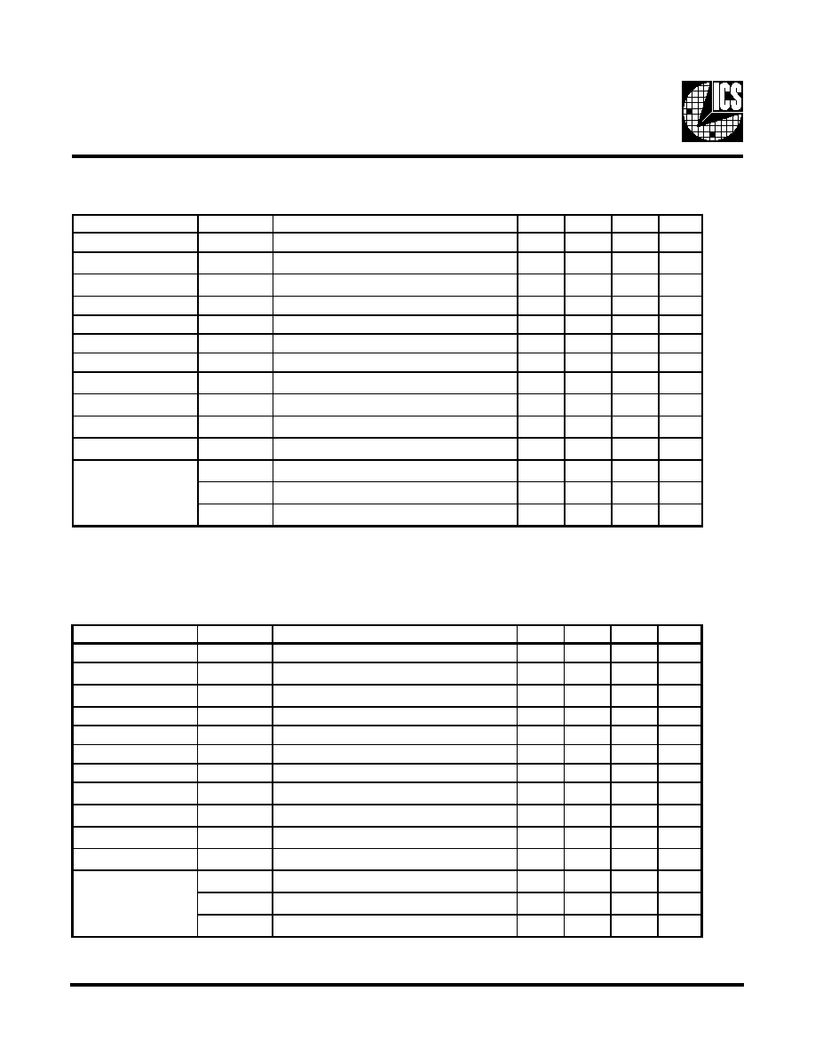
Power-On Conditions
Example:
a) if MODE = 1, pins 26 and 27 are configured as SDRAM7 and SDRAM6 respectively.
b) if MODE = 0, pins 26 and 27 are configured as PCI_STOP# and CPU_STOP# respectively.
Power-On Default Conditions
At power-up and before device programming, all clocks will default to an enabled and on condition. The frequencies that are then produced
are on the MODE pin as shown in the table below.
K
C
O
L
C
P
U
-
R
E
W
O
P
T
A
N
O
I
T
I
D
N
O
C
T
L
U
A
F
E
D
)
1
:
0
(
F
E
R
z
H
M
8
1
8
1
3
.
4
1
0
C
I
P
A
O
I
z
H
M
8
1
8
1
3
.
4
1
z
H
M
4
2
/
8
4
z
H
M
8
4
#
0
6
/
6
6
L
E
S
E
D
O
M
#
N
I
P
N
O
I
T
P
I
R
C
S
E
D
N
O
I
T
C
N
U
F
1
1
2
4
,
1
4
,
9
3
,
8
3
s
K
L
C
U
P
C
e
l
b
a
s
i
d
/
e
l
b
a
n
e
g
i
f
n
o
c
l
a
i
r
e
s
/
w
-
z
H
M
6
.
6
6
,
2
3
,
3
3
,
5
3
,
6
3
6
2
,
7
2
,
9
2
,
0
3
M
A
R
D
S
s
t
u
p
t
u
o
M
A
R
D
S
l
l
A
-
z
H
M
6
.
6
6
,
2
1
,
3
1
,
4
1
,
6
1
8
,
9
,
1
1
s
K
L
C
I
C
P
e
l
b
a
s
i
d
/
e
l
b
a
n
e
g
i
f
n
o
c
l
a
i
r
e
s
/
w
-
z
H
M
3
.
3
3
0
1
2
4
,
1
4
,
9
3
,
8
3
s
K
L
C
U
P
C
e
l
b
a
s
i
d
/
e
l
b
a
n
e
g
i
f
n
o
c
l
a
i
r
e
s
/
w
-
z
H
M
0
6
,
2
3
,
3
3
,
5
3
,
6
3
6
2
,
7
2
,
9
2
,
0
3
M
A
R
D
S
e
l
b
a
s
i
d
/
e
l
b
a
n
e
g
i
f
n
o
c
l
a
i
r
e
s
/
w
-
z
H
M
0
6
,
2
1
,
3
1
,
4
1
,
6
1
8
,
9
,
1
1
s
K
L
C
I
C
P
e
l
b
a
s
i
d
/
e
l
b
a
n
e
g
i
f
n
o
c
l
a
i
r
e
s
/
w
-
z
H
M
0
3
1
0
6
2
#
P
O
T
S
_
I
C
P
s
k
c
o
l
C
)
5
:
0
(
I
C
P
,
t
n
e
m
e
g
a
n
a
M
r
e
w
o
P
w
o
l
n
e
h
w
d
e
p
p
o
t
S
7
2
#
P
O
T
S
_
U
P
C
s
k
c
o
l
C
)
5
:
0
(
U
P
C
,
t
n
e
m
e
g
a
n
a
M
r
e
w
o
P
w
o
l
n
e
h
w
d
e
p
p
o
t
S
8
F
_
K
L
C
I
C
P
r
o
f
g
n
i
n
n
u
r
e
e
r
F
k
c
o
l
C
I
C
P
-
z
H
M
3
.
3
3
-
z
H
M
3
.
3
3
t
n
e
m
e
g
a
n
a
M
r
e
w
o
P
2
4
,
1
4
,
9
3
,
8
3
s
K
L
C
U
P
C
d
n
a
l
o
r
t
n
o
C
p
o
t
S
l
a
n
r
e
t
x
e
/
w
s
k
c
o
l
C
U
P
C
-
z
H
M
6
.
6
6
.
e
l
b
a
s
i
d
/
e
l
b
a
n
e
l
a
u
d
i
v
i
d
n
i
g
i
f
n
o
c
l
a
i
r
e
s
,
2
3
,
3
3
,
5
3
,
6
3
9
2
,
0
3
M
A
R
D
S
l
a
u
d
i
v
i
d
n
i
g
i
f
n
o
c
l
a
i
r
e
s
/
w
s
k
c
o
l
C
M
A
R
D
S
-
z
H
M
6
.
6
6
.
e
l
b
a
s
i
d
/
e
l
b
a
n
e
,
2
1
,
3
1
,
4
1
,
6
1
9
,
1
1
s
K
L
C
I
C
P
d
n
a
l
o
r
t
n
o
c
p
o
t
S
l
a
n
r
e
t
x
e
/
w
s
k
c
o
l
C
I
C
P
-
z
H
M
3
.
3
3
.
e
l
b
a
s
i
d
/
e
l
b
a
n
e
l
a
u
d
i
v
i
d
n
i
g
i
f
n
o
c
l
a
i
r
e
s
0
0
6
2
#
P
O
T
S
_
I
C
P
s
k
c
o
l
C
)
5
:
0
(
I
C
P
,
t
n
e
m
e
g
a
n
a
M
r
e
w
o
P
w
o
l
n
e
h
w
d
e
p
p
o
t
S
7
2
#
P
O
T
S
_
U
P
C
s
k
c
o
l
C
)
5
:
0
(
U
P
C
,
t
n
e
m
e
g
a
n
a
M
r
e
w
o
P
w
o
l
n
e
h
w
d
e
p
p
o
t
S
8
F
_
K
L
C
I
C
P
r
e
w
o
P
r
o
f
g
n
i
n
n
u
r
e
e
r
F
k
c
o
l
C
I
C
P
-
z
H
M
0
3
t
n
e
m
e
g
a
n
a
M
2
4
,
1
4
,
9
3
,
8
3
s
K
L
C
U
P
C
d
n
a
l
o
r
t
n
o
c
p
o
t
S
l
a
n
r
e
t
x
e
/
w
s
k
c
o
l
C
U
P
C
-
z
H
M
0
6
.
e
l
b
a
s
i
d
/
e
l
b
a
n
e
l
a
u
d
i
v
i
d
n
i
g
i
f
n
o
c
l
a
i
r
e
s
,
2
3
,
3
3
,
5
3
,
6
3
9
2
,
0
3
M
A
R
D
S
l
a
u
d
i
v
i
d
n
i
g
i
f
n
o
c
l
a
i
r
e
s
/
w
s
k
c
o
l
C
M
A
R
D
S
-
z
H
M
0
6
.
e
l
b
a
s
i
d
/
e
l
b
a
n
e
,
2
1
,
3
1
,
4
1
,
6
1
9
,
1
1
s
K
L
C
I
C
P
d
n
a
l
o
r
t
n
o
c
p
o
t
S
l
a
n
r
e
t
x
e
/
w
s
k
c
o
l
C
I
C
P
-
z
H
M
0
3
.
e
l
b
a
s
i
d
/
e
l
b
a
n
e
l
a
u
d
i
v
i
d
n
i
g
i
f
n
o
c
l
a
i
r
e
s

4
ICS9148-02
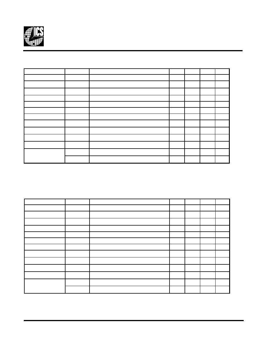
Technical Pin Function Descriptions
VDD(1,2,3,4)
This is the power supply to the internal core logic of the
device as well as the clock output buffers for REF(0:1),
PCICLK, 48/24MHzA/B and SDRAM(0:7).
This pin operates at 3.3V volts. Clocks from the listed
buffers that it supplies will have a voltage swing from Ground
to this level. For the actual guaranteed high and low voltage
levels for the Clocks, please consult the DC parameter table
in this data sheet.
VDDL1,2
This is the power supplies for the CPUCLK and IOAPCI
output buffers. The voltage level for these outputs may be
2.5 or 3.3volts. Clocks from the buffers that each supplies
will have a voltage swing from Ground to this level. For the
actual Guaranteed high and low voltage levels of these
Clocks, please consult the DC parameter table in this Data
Sheet.
GND
This is the power supply ground (common or negative) return
pin for the internal core logic and all the output buffers.
X1
This input pin serves one of two functions. When the device
is used with a Crystal, X1 acts as the input pin for the
reference signal that comes from the discrete crystal. When
the device is driven by an external clock signal, X1 is the
device input pin for that reference clock. This pin also
implements an internal Crystal loading capacitor that is
connected to ground. See the data tables for the value of this
capacitor.
X2
This Output pin is used only when the device uses a Crystal
as the reference frequency source. In this mode of operation,
X2 is an output signal that drives (or excites) the discrete
Crystal. The X2 pin will also implement an internal Crystal
loading capacitor that is connected to ground. See the Data
Sheet for the value of this capacitor.
CPUCLK (0:3)
These Output pins are the Clock Outputs that drive processor
and other CPU related circuitry that requires clocks which
are in tight skew tolerance with the CPU clock. The voltage
swing of these Clocks are controlled by the Voltage level
applied to the VDDL2 pin of the device. See the Functionality
Table for a list of the specific frequencies that are available
for these Clocks and the selection codes to produce them.
SDRAM(0:7)
These Output Clocks are use to drive Dynamic RAMs and
are low skew copies of the CPU Clocks. The voltage swing
of the SDRAMs output is controlled by the supply voltage
that is applied to VDD3 of the device, operates at 3.3 volts.
48/24MHzA, B
This is a fixed frequency Clock output that is typically used
to drive Super I/O devices. Outputs A and B are defined as
24 or 48MHz by I
2
C register (see table).
IOAPIC
This Output is a fixed frequency Output Clock that runs at the
Reference Input (typically 14.31818MHz) . Its voltage level
swing is controlled by VDDL1 and may operate at 2.5 or
3.3volts.
REF(0:1)
The REF Outputs are fixed frequency Clocks that run at the
same frequency as the Input Reference Clock X1 or the
Crystal (typically 14.31818MHz) attached across X1 and
X2.
PCICLK_F
This Output is equal to PCICLK(0:5) and is FREE RUNNING,
and will not be stopped by PCI_STP#.
PCICLK (0:5)
These Output Clocks generate all the PCI timing requirements
for a Pentium/Pro based system. They conform to the
current PCI specification. They run at 1/2 CPU frequency.
SELECT 66.6/60MHz#
This Input pin controls the frequency of the Clocks at the
CPU, PCICLK and SDRAM output pins. If a logic 1 value
is present on this pin, the 66.6 MHz Clock will be selected.
If a logic 0 is used, the 60MHz frequency will be selected.
MODE
This Input pin is used to select the Input function of the I/
O pins. An active Low will place the I/O pins in the Input
mode and enable those stop clock functions.

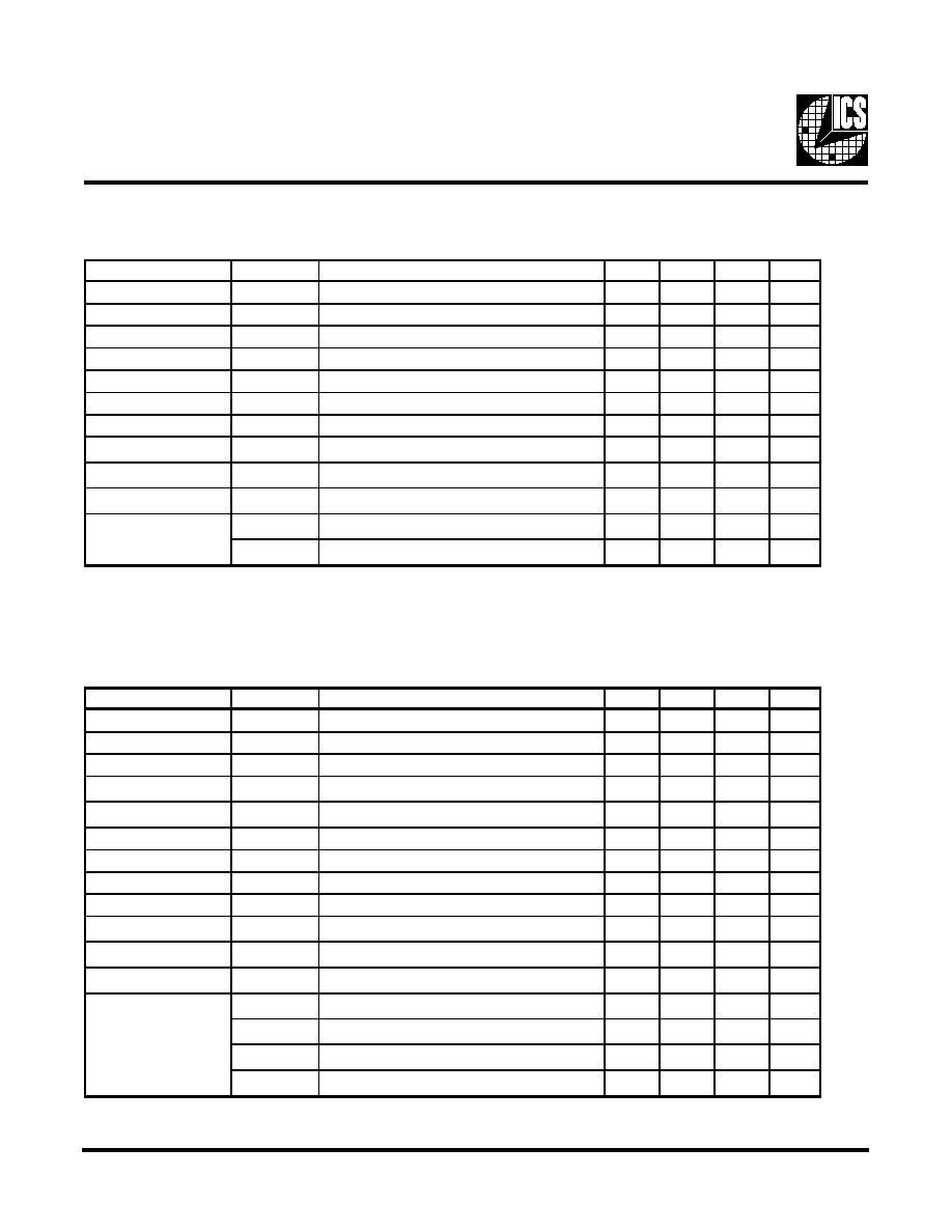
5
ICS9148-02
CPU 3.3_2.5#
This Input pin controls the CPU and IOAPIC output buffer
strength for skew matching CPU and SDRAM outputs to
compensate for the external VDDL supply condition. It is
important to use this function when selecting power supply
requirements for VDDL1,2. A logic 0 (ground) will indicate
2.5V operation and a logic 1 will indicate 3.3V operation.
This pin has an internal pullup resistor to VDD.
PWR_DWN#
This is an asynchronous active Low Input pin used to Power
Down the device into a Low Power state by not removing the
power supply. The internal Clocks are disabled and the VCO
and Crystal are stopped. Powered Down will also place all
the Outputs in a low state at the end of their current cycle.
The latency of Power Down will not be greater than 3ms. The
I
2
C inputs will be Tri-Stated and the device will retain all
programming information. This input pin only valid when
MODE=0 (Power Management Mode)
CPU_STOP#
This is a synchronous active Low Input pin used to stop the
CPUCLK clocks in an active low state. All other Clocks
including SDRAM clocks will continue to run while this
function is enabled. The CPUCLKs will have a turn ON
latency of at least 3 CPU clocks. This input pin only valid
when MODE=0 (Power Management Mode)
PCI_STOP#
This is a synchronous active Low Input pin used to stop the
PCICLK clocks in an active low state. It will not effect
PCICLK_F nor any other outputs. This input pin only valid
when MODE=0 (Power Management Mode)
I
2
C
The SDATA and SCLOCK Inputs are use to program the
device. The clock generator is a slave-receiver device in the
I
2
C protocol. It will allow read-back of the registers. See
configuration map for register functions. The I
2
C
specification in Philips I
2
C Peripherals Data Handbook
(1996) should be followed.
Technical Pin Function Descriptions
6
ICS9148-02
Serial Configuration Command Bitmaps
Byte 0: Functional and Frequency Select Clock Register (default on Bits 7, 6, 5, 4, 1, 0 = 0)
(default on Bits 3, 2 = 1)
General I
2
C serial interface information
A.
For the clock generator to be addressed by an I
2
C controller, the following address must be sent as a start sequence, with
an acknowledge bit between each byte.
B.
The clock generator is a slave/receiver I
2
C component. It can "read back "(in Philips I
2
C protocol) the data stored in the
latches for verification. (set R/W# to 1 above). There is no BYTE count supported, so it does not meet the Intel SMB
PIIX4 protocol.
C.
The data transfer rate supported by this clock generator is 100K bits/sec (standard mode)
D.
The input is operating at 3.3V logic levels.
E.
The data byte format is 8 bit bytes.
F.
To simplify the clock generator I
2
C interface, the protocol is set to use only block writes from the controller. The bytes
must be accessed in sequential order from lowest to highest byte with the ability to stop after any complete byte has
been transferred. The Command code and Byte count shown above must be sent, but the data is ignored for those two
bytes. The data is loaded until a Stop sequence is issued.
G.
In the power down mode (PWR_DWN# Low), the SDATA and SCLK pins are tristated and the internal data latches
maintain all prior programming information.
H.
At power-on, all registers are set to a default condition. See Byte 0 detail for default condition, Bytes 1 through 5 default
to a 1 (Enabled output state)
Then Byte 0, 1, 2, etc in
sequence until STOP.
Byte 0, 1, 2, etc in sequence until STOP.
Note: PWD = Power-Up Default
I
2
C is a trademark of
Philips Corporation
T
I
B
#
N
I
P
N
O
I
T
P
I
R
C
S
E
D
D
W
P
7
t
i
B
-
d
e
v
r
e
s
e
R
0
6
t
i
B
-
n
o
i
t
a
r
e
p
o
l
a
m
r
o
n
r
o
f
0
e
b
t
s
u
M
0
5
t
i
B
-
e
p
y
t
s
l
o
r
t
n
o
C
,
m
u
r
t
c
e
p
S
d
a
e
r
p
S
n
I
)
d
a
e
r
p
s
n
w
o
d
=
1
,
d
e
r
e
t
n
e
c
=
0
(
0
4
t
i
B
g
n
i
d
a
e
r
p
S
s
l
o
r
t
n
o
C
,
m
u
r
t
c
e
p
S
d
a
e
r
p
S
n
I
)
%
6
.
0
=
1
%
8
.
1
=
0
(
0
3
t
i
B
3
2
z
H
M
4
2
=
0
,
z
H
M
8
4
=
1
)
t
c
e
l
e
S
y
c
n
e
u
q
e
r
F
(
z
H
M
4
2
/
8
4
1
2
t
i
B
2
2
z
H
M
4
2
=
0
,
z
H
M
8
4
=
1
)
t
c
e
l
e
S
y
c
n
e
u
q
e
r
F
(
z
H
M
4
2
/
8
4
1
1
t
i
B
0
t
i
B
-
1
t
i
B
1
1
0
0
0
t
i
B
e
t
a
t
S
-
i
r
T
-
1
e
l
b
a
n
E
m
u
r
t
c
e
p
S
d
a
e
r
p
S
-
0
e
d
o
m
t
s
e
T
-
1
n
o
i
t
a
r
e
p
o
l
a
m
r
o
N
-
0
0
0
r
o
t
a
r
e
n
e
G
k
c
o
l
C
)
s
t
i
b
7
(
s
s
e
r
d
d
A
K
C
A
y
m
m
u
d
s
t
i
b
8
+
e
d
o
c
d
n
a
m
m
o
c
K
C
A
y
m
m
u
d
s
t
i
b
8
+
t
n
u
o
c
e
t
y
B
K
C
A
#
W
/
R
&
)
0
:
6
(
A
2
D
)
H
(
r
o
t
a
r
e
n
e
G
k
c
o
l
C
)
s
t
i
b
7
(
s
s
e
r
d
d
A
K
C
A
0
e
t
y
B
K
C
A
1
e
t
y
B
K
C
A
#
W
/
R
&
)
0
:
6
(
A
3
D
)
H
(
7
ICS9148-02
Notes:
1. TCLK is a test clock driven on the X1 (crystal in pin) input during test mode.
y
t
i
l
a
n
o
i
t
c
n
u
F
U
P
C
,
I
C
P
F
_
I
C
P
M
A
R
D
S
F
E
R
C
I
P
A
O
I
z
H
M
4
2
n
o
i
t
c
e
l
e
S
z
H
M
8
4
n
o
i
t
c
e
l
e
S
e
t
a
t
s
i
r
T
Z
-
I
H
Z
-
I
H
Z
-
I
H
Z
-
I
H
Z
-
I
H
Z
-
I
H
Z
-
I
H
e
d
o
m
t
s
e
T
2
/
K
L
C
T
1
4
/
K
L
C
T
1
2
/
K
L
C
T
1
K
L
C
T
1
K
L
C
T
1
4
/
K
L
C
T
1
2
/
K
L
C
T
1
Byte 1: CPU, 24/48 MHz Clock Register
Notes: 1 = Enabled; 0 = Disabled, outputs held low
Byte 2: PCICLK Clock Register
Byte 4: SDRAM Clock Register
Notes: 1 = Enabled; 0 = Disabled, outputs held low
Notes: 1 = Enabled; 0 = Disabled, outputs held low
T
I
B
#
N
I
P
D
W
P
N
O
I
T
P
I
R
C
S
E
D
7
t
i
B
-
1
d
e
v
r
e
s
e
R
6
t
i
B
8
1
)
t
c
a
n
I
/
t
c
A
(
F
_
K
L
C
I
C
P
5
t
i
B
6
1
1
)
t
c
a
n
I
/
t
c
A
(
5
K
L
C
I
C
P
4
t
i
B
4
1
1
)
t
c
a
n
I
/
t
c
A
(
4
K
L
C
I
C
P
3
t
i
B
3
1
1
)
t
c
a
n
I
/
t
c
A
(
3
K
L
C
I
C
P
2
t
i
B
2
1
1
)
t
c
a
n
I
/
t
c
A
(
2
K
L
C
I
C
P
1
t
i
B
1
1
1
)
t
c
a
n
I
/
t
c
A
(
1
K
L
C
I
C
P
0
t
i
B
9
1
)
t
c
a
n
I
/
t
c
A
(
0
K
L
C
I
C
P
T
I
B
#
N
I
P
D
W
P
N
O
I
T
P
I
R
C
S
E
D
7
t
i
B
-
1
d
e
v
r
e
s
e
R
6
t
i
B
-
1
d
e
v
r
e
s
e
R
5
t
i
B
-
1
d
e
v
r
e
s
e
R
4
t
i
B
-
1
d
e
v
r
e
s
e
R
3
t
i
B
-
1
d
e
v
r
e
s
e
R
2
t
i
B
-
1
d
e
v
r
e
s
e
R
1
t
i
B
-
1
d
e
v
r
e
s
e
R
0
t
i
B
-
1
d
e
v
r
e
s
e
R
T
I
B
#
N
I
P
D
W
P
N
O
I
T
P
I
R
C
S
E
D
7
t
i
B
3
2
1
)
t
c
a
n
I
/
t
c
A
(
z
H
M
4
2
/
8
4
6
t
i
B
2
2
1
)
t
c
a
n
I
/
t
c
A
(
z
H
M
4
2
/
8
4
5
t
i
B
-
1
d
e
v
r
e
s
e
R
4
t
i
B
-
1
d
e
v
r
e
s
e
R
3
t
i
B
8
3
1
)
t
c
a
n
I
/
t
c
A
(
3
K
L
C
U
P
C
2
t
i
B
9
3
1
)
t
c
a
n
I
/
t
c
A
(
2
K
L
C
U
P
C
1
t
i
B
1
4
1
)
t
c
a
n
I
/
t
c
A
(
1
K
L
C
U
P
C
0
t
i
B
2
4
1
)
t
c
a
n
I
/
t
c
A
(
0
K
L
C
U
P
C
Byte 3: SDRAM Clock Register
Notes: 1 = Enabled; 0 = Disabled, outputs held low
T
I
B
#
N
I
P
D
W
P
N
O
I
T
P
I
R
C
S
E
D
7
t
i
B
6
2
1
)
t
c
a
n
I
/
t
c
A
(
7
M
A
R
D
S
6
t
i
B
7
2
1
)
t
c
a
n
I
/
t
c
A
(
6
M
A
R
D
S
5
t
i
B
9
2
1
)
t
c
a
n
I
/
t
c
A
(
5
M
A
R
D
S
4
t
i
B
0
3
1
)
t
c
a
n
I
/
t
c
A
(
4
M
A
R
D
S
3
t
i
B
2
3
1
)
t
c
a
n
I
/
t
c
A
(
3
M
A
R
D
S
2
t
i
B
3
3
1
)
t
c
a
n
I
/
t
c
A
(
2
M
A
R
D
S
1
t
i
B
5
3
1
)
t
c
a
n
I
/
t
c
A
(
1
M
A
R
D
S
0
t
i
B
6
3
1
)
t
c
a
n
I
/
t
c
A
(
0
M
A
R
D
S
Select Functions
Note: PWD = Power-Up Default
8
ICS9148-02
Power Management
ICS9148-02 Power Management Requirements
Clock Enable Configuration
Full clock cycle timing is guaranteed at all times after the system has initially powered up except where noted. During power
up and power down operations using the PWR PD# select pin will not cause clocks of a short or longer pulse than that of the
running clock. The first clock pulse coming out of a stopped clock condition may be slightly distorted due to clock network
charging circuitry. Board routing and signal loading may have a large impact on the initial clock distortion also.
Notes.
1. Clock on latency is defined from when the clock enable goes active to when the first valid clock comes out of the device.
2. Clock off latency is defined from when the clock enable goes inactive to when the last clock is driven low out of the device.
3. Power up latency is when PD# goes inactive (high) to when the first valid clocks are output by the device.
4. Power down has controlled clock counts applicable to CPUCLK, SDRAM, PCICLK only.
The REF and IOAPIC will be stopped independant of these.
L
A
N
G
I
S
E
T
A
T
S
L
A
N
G
I
S
y
c
n
e
t
a
L
g
n
i
n
n
u
r
e
e
r
f
f
o
s
e
g
d
e
g
n
i
s
i
r
f
o
.
o
N
K
L
C
I
C
P
#
P
O
T
S
_
U
P
C
)
d
e
l
b
a
s
i
D
(
0
2
1
)
d
e
l
b
a
n
E
(
1
1
1
#
P
O
T
S
_
I
C
P
)
d
e
l
b
a
s
i
D
(
0
2
1
)
d
e
l
b
a
n
E
(
1
1
1
#
N
W
D
_
R
W
P
)
n
o
i
t
a
r
e
p
O
l
a
m
r
o
N
(
1
3
S
m
3
)
n
w
o
D
r
e
w
o
P
(
0
4
x
a
m
2
Byte 5: Peripheral Clock Register
Notes: 1 = Enabled; 0 = Disabled, outputs held low
T
I
B
#
N
I
P
D
W
P
N
O
I
T
P
I
R
C
S
E
D
7
t
i
B
-
1
d
e
v
r
e
s
e
R
6
t
i
B
-
1
d
e
v
r
e
s
e
R
5
t
i
B
-
1
d
e
v
r
e
s
e
R
4
t
i
B
5
4
1
)
t
c
a
n
I
/
t
c
A
(
0
C
I
P
A
O
I
3
t
i
B
-
1
d
e
v
r
e
s
e
R
2
t
i
B
-
1
d
e
v
r
e
s
e
R
1
t
i
B
1
1
)
t
c
a
n
I
/
t
c
A
(
1
F
E
R
0
t
i
B
2
1
)
t
c
a
n
I
/
t
c
A
(
0
F
E
R
#
P
O
T
S
_
U
P
C
#
P
O
T
S
_
I
C
P
#
N
W
D
_
R
W
P
K
L
C
U
P
C
K
L
C
I
C
P
,
s
k
c
o
l
C
r
e
h
t
O
,
M
A
R
D
S
,
F
E
R
,
s
C
I
P
A
O
I
A
z
H
M
4
2
/
8
4
B
z
H
M
4
2
/
8
4
l
a
t
s
y
r
C
s
O
C
V
X
X
0
w
o
L
w
o
L
d
e
p
p
o
t
S
f
f
O
f
f
O
0
0
1
w
o
L
w
o
L
g
n
i
n
n
u
R
g
n
i
n
n
u
R
g
n
i
n
n
u
R
0
1
1
w
o
L
z
H
M
0
3
/
3
.
3
3
g
n
i
n
n
u
R
g
n
i
n
n
u
R
g
n
i
n
n
u
R
1
0
1
z
H
M
0
6
/
6
.
6
6
w
o
L
g
n
i
n
n
u
R
g
n
i
n
n
u
R
g
n
i
n
n
u
R
1
1
1
z
H
M
0
6
/
6
.
6
6
z
H
M
0
3
/
3
.
3
3
g
n
i
n
n
u
R
g
n
i
n
n
u
R
g
n
i
n
n
u
R
Note: PWD = Power-Up Default
Byte 6: Optional Register for Future
Notes:
1. Byte 6 is reserved by Integrated Circuit Systems for
future applications.
T
I
B
#
N
I
P
D
W
P
N
O
I
T
P
I
R
C
S
E
D
7
t
i
B
-
1
d
e
v
r
e
s
e
R
6
t
i
B
-
1
d
e
v
r
e
s
e
R
5
t
i
B
-
1
d
e
v
r
e
s
e
R
4
t
i
B
-
1
d
e
v
r
e
s
e
R
3
t
i
B
-
1
d
e
v
r
e
s
e
R
2
t
i
B
-
1
d
e
v
r
e
s
e
R
1
t
i
B
-
1
d
e
v
r
e
s
e
R
0
t
i
B
-
1
d
e
v
r
e
s
e
R
9
ICS9148-02
PCI_STOP# Timing Diagram
PCI_STOP# is an asynchronous input to the ICS9148-02. It is used to turn off the PCICLK (0:5) clocks for low power
operation. PCI_STOP# is synchronized by the ICS9148-02 internally. The minimum that the PCICLK (0:5) clocks are enabled
(PCI_STOP# high pulse) is at least 10 PCICLK (0:5) clocks. PCICLK (0:5) clocks are stopped in a low state and started with
a full high pulse width guaranteed. PCICLK (0:5) clock on latency cycles are only one rising PCICLK clock off latency is one
PCICLK clock.
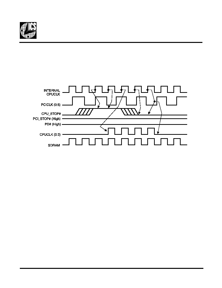
CPU_STOP# Timing Diagram
CPUSTOP# is an asychronous input to the clock synthesizer. It is used to turn off the CPUCLKs for low power operation.
CPU_STOP# is synchronized by the ICS9148-02. The minimum that the CPUCLK is enabled (CPU_STOP# high pulse) is
100 CPUCLKs. All other clocks will continue to run while the CPUCLKs are disabled. The CPUCLKs will always be stopped
in a low state and start in such a manner that guarantees the high pulse width is a full pulse. CPUCLK on latency is less than
4 CPUCLKs and CPUCLK off latency is less than 4 CPUCLKs.
(Drawing shown on next page.)
Notes:
1. All timing is referenced to the internal CPUCLK.
2. CPU_STOP# is an asynchronous input and metastable conditions may exist.
This signal is synchronized to the CPUCLKs inside the ICS9148-02.
3. All other clocks continue to run undisturbed.
4. PD# and PCI_STOP# are shown in a high (true) state.
10
ICS9148-02
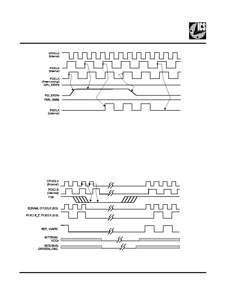
PD# Timing Diagram
The power down selection is used to put the part into a very low power state without turning off the power to the part. PD# is
an asynchronous active low input. This signal is synchronized internal by the ICS9148-02 prior to its control action of
powering down the clock synthesizer. Internal clocks will not be running after the device is put in power down state. When PD#
is active (low) all clocks are driven to a low state and held prior to turning off the VCOs and the Crystal oscillator. The power
on latency is guaranteed to be less than 3mS. The power down latency is less than three CPUCLK cycles. PCI_STOP# and
CPU_STOP# are dont care signals during the power down operations.
Notes:
1. All timing is referenced to the Internal CPUCLK (defined as inside the ICS9148 device).
2. PD# is an asynchronous input and metastable conditions may exist. This signal is synchronized inside the ICS9148.
3. The shaded sections on the VCO and the Crystal signals indicate an active clock is being generated.
Notes:
1. All timing is referenced to the Internal CPUCLK (defined as inside the ICS9148 device.)
2. PCI_STOP# is an asynchronous input, and metastable conditions may exist. This signal is required to be synchronized
inside the ICS9148.
3. All other clocks continue to run undisturbed.
4. PD# and CPU_STOP# are shown in a high (true) state.
11
ICS9148-02
Absolute Maximum Ratings
Supply Voltage . . . . . . . . . . . . . . . . . . . . . . . . . . . 7.0 V
Logic Inputs . . . . . . . . . . . . . . . . . . . . . . . . . . . . GND 0.5 V to V
DD
+0.5 V
Ambient Operating Temperature . . . . . . . . . . . . 0°C to +70°C
Storage Temperature . . . . . . . . . . . . . . . . . . . . . . 65°C to +150°C
Stresses above those listed under Absolute Maximum Ratings may cause permanent damage to the device. These ratings are
stress specifications only and functional operation of the device at these or any other conditions above those listed in the
operational sections of the specifications is not implied. Exposure to absolute maximum rating conditions for extended periods
may affect product reliability.
Electrical Characteristics - Input/Supply/Common Output Parameters
T
A
= 0 - 70C; Supply Voltage V
DD
= V
DDL
= 3.3 V +/-5% (unless otherwise stated)
PARAMETER
SYMBOL
CONDITIONS
MIN
TYP
MAX
UNITS
Input High Voltage
V
IH
2
V
DD
+0.3
V
Input Low Voltage
V
IL
V
SS
-0.3
0.8
V
Input High Current
I
IH
V
IN
= V
DD
0.1
5
µ
A
Input Low Current
I
IL1
V
IN
= 0 V; Inputs with no pull-up resistors
-5
2.0
µ
A
Input Low Current
I
IL2
V
IN
= 0 V; Inputs with pull-up resistors
-200
-100
µ
A
Operating
I
DD3.3OP
C
L
= 0 pF; Select @ 66M
60
100
mA
Supply Current
Power Down
I
DD3.3P D
C
L
= 0 pF; With input address to Vdd or GND
400
600
µ
A
Supply Current
Input frequency
F
i
V
DD
= 3.3 V;
14.318
MHz
Input Capacitance
1
C
IN
Logic Inputs
5
pF
C
INX
X1 & X2 pins
27
36
45
ps
Transition Time
1
T
trans
To 1st crossing of target Freq.
3
ms
Settling Time
1
T
s
From 1st crossing to 1% target Freq.
ms
Clk Stabilization
1
T
STAB
From V
DD
= 3.3 V to 1% target Freq.
3
ms
Skew
1
T
CP U-SDRAM1
V
T
= 1.5 V
200
500
ps
T
CP U-P CI1
V
T
= 1.5 V;
1.5
3.2
4.5
ns
1
Guaranteed by design, not 100% tested in production.
Electrical Characteristics - Input/Supply/Common Output Parameters
T
A
= 0 - 70C; Supply Voltage V
DD
= 3.3 V +/-5%, V
DDL
= 2.5 V +/-5% (unless otherwise stated)
PARAMETER
SYMBOL
CONDITIONS
MIN
TYP
MAX
UNITS
Operating
I
DD2.5OP
C
L
= 0 pF; Select @ 66M
5
20
mA
Supply Current
Power Down
I
DD2.5P D
C
L
= 0 pF;
0.21
1.0
µ
A
Supply Current
Skew
1
T
CP U-SDRAM2
V
T
= 1.5 V; V
TL
= 1.25 V; SDRAM Leads
150
500
ps
T
CP U-P CI2
V
T
= 1.5 V; V
TL
= 1.25 V; CPU Leads
1
2.8
4
ns
1
Guaranteed by design, not 100% tested in production.
12
ICS9148-02
Electrical Characteristics - CPU
T
A
= 0 - 70C; V
DD
= V
DDL
= 3.3 V +/-5%; C
L
= 10 - 20 pF (unless otherwise stated)
PARAMETER
SYMBOL
CONDITIONS
MIN
TYP
MAX UNITS
Output Frequency
F
O2
60
66
MHz
Output Impedance
R
DSP 2A
1
V
O
= V
DD
*(0.5)
10
20
Output Impedance
R
DSN2A
1
V
O
= V
DD
*(0.5)
10
20
Output High Voltage
V
OH2A
I
OH
= -28 mA
2.4
2.5
V
Output Low Voltage
V
OL2A
I
OL
= 27 mA
0.35
0.4
V
Output High Current
I
OH2A
V
OH
= 2.0 V
-52
-48
mA
Output Low Current
I
OL2A
V
OL
= 0.8 V
49.3
59
mA
Rise Time
t
r2A
1
V
OL
= 0.4 V, V
OH
= 2.4 V
1.1
2.85
ns
Fall Time
t
f2A
1
V
OH
= 2.4 V, V
OL
= 0.4 V
0.95
2.85
ns
Duty Cycle
d
t2A
1
V
T
= 1.5 V
45
51
55
%
Skew
t
sk2A
1
V
T
= 1.5 V
80
250
ps
t
jcyc-cyc2A
1
V
T
= 1.5 V
170
250
ps
Jitter
t
j1s2A
1
V
T
= 1.5 V
60
150
ps
t
jabs2A
1
V
T
= 1.5 V
-250
100
+250
ps
1
Guaranteed by design, not 100% tested in production.
Electrical Characteristics - CPU
T
A
= 0 - 70C; V
DD
= 3.3 V +/-5%, V
DDL
= 2.5 V +/-5%; C
L
= 10 - 20 pF (unless otherwise stated)
PARAMETER
SYMBOL
CONDITIONS
MIN
TYP
MAX UNITS
Output Frequency
F
O2
60
66
MHz
Output Impedance
R
DSP 2B
1
V
O
= V
DD
*(0.5)
10
25
Output Impedance
R
DSN2B
1
V
O
= V
DD
*(0.5)
10
25
Output High Voltage
V
OH2B
I
OH
= -13.0 mA
2
2.2
V
Output Low Voltage
V
OL2B
I
OL
= 14 mA
0.3
0.4
V
Output High Current
I
OH2B
V
OH
= 1.7 V
-20
-16
mA
Output Low Current
I
OL2B
V
OL
= 0.7 V
22
26
mA
Rise Time
t
r2B
1
V
OL
= 0.4 V, V
OH
= 2.0 V
1.42
1.6
ns
Fall Time
t
f2B
1
V
OH
= 2.0 V, V
OL
= 0.4 V
0.95
1.6
ns
Duty Cycle
d
t2B
1
V
T
= 1.25 V
45
49.5
55
ns
Skew
t
sk2B
1
V
T
= 1.25 V
60
250
ps
t
jcyc-cyc2B
1
V
T
= 1.25 V
150
250
ps
Jitter
t
j1s2B
1
V
T
= 1.25 V
80
150
ps
t
jabs2B
1
V
T
= 1.25 V
-250
80
+250
ps
1
Guaranteed by design, not 100% tested in production.
13
ICS9148-02
Electrical Characteristics - PCI
T
A
= 0 - 70C; V
DD
= V
DDL
= 3.3 V +/-5%; C
L
= 30 pF (unless otherwise stated)
PARAMETER
SYMBOL
CONDITIONS
MIN
TYP
MAX UNITS
Output Frequency
F
O1
30
-
33
MHz
Output Impedance
R
DSP 1
1
V
O
= V
DD
*(0.5)
12
55
Output Impedance
R
DSN1
1
V
O
= V
DD
*(0.5)
12
55
Output High Voltage
V
OH1
I
OH
= -14.5 mA
2.4
2.7
V
Output Low Voltage
V
OL1
I
OL
= 9.4 mA
0.2
0.4
V
Output High Current
I
OH1
V
OH
= 2.0 V
-47
-22
mA
Output Low Current
I
OL1
V
OL
= 0.8 V
17.1
47.5
mA
Rise Time
t
r1
1
V
OL
= 0.4 V, V
OH
= 2.4 V
1.5
2
ns
Fall Time
t
f1
1
V
OH
= 2.4 V, V
OL
= 0.4 V
1.1
2
ns
Duty Cycle
d
t1
1
V
T
= 1.5 V
45
51
55
%
Skew
t
sk1
1
V
T
= 1.5 V
100
500
ps
Jitter
t
j1s1
1
V
T
= 1.5 V
50
150
ps
t
jabs1
1
V
T
= 1.5 V
-250
120
250
ps
1
Guaranteed by design, not 100% tested in production.
Electrical Characteristics - SDRAM
T
A
= 0 - 70C; V
DD
= V
DDL
= 3.3 V +/-5%; C
L
= 20 - 30 pF (unless otherwise stated)
PARAMETER
SYMBOL
CONDITIONS
MIN
TYP
MAX UNITS
Output Frequency
F
O3
60
66
MHz
Output Impedance
R
DSP 3
1
V
O
= V
DD
*(0.5)
10
24
Output Impedance
R
DSN3
1
V
O
= V
DD
*(0.5)
10
24
Output High Voltage
V
OH3
I
OH
= -24 mA
2.4
2.5
V
Output Low Voltage
V
OL3
I
OL
= 23 mA
0.35
0.4
V
Output High Current
I
OH3
V
OH
= 2.0 V
-47
-40
mA
Output Low Current
I
OL3
V
OL
= 0.8 V
41
47.5
mA
Rise Time
T
r3
1
V
OL
= 0.4 V, V
OH
= 2.4 V
1.45
1.7
ns
Fall Time
T
f3
1
V
OH
= 2.4 V, V
OL
= 0.4 V
1.2
1.5
ns
Duty Cycle
D
t3
1
V
T
= 1.5 V
45
51
55
%
Skew
T
sk3
1
V
T
= 1.5 V
80
500
ps
Jitter
T
j1s3
1
V
T
= 1.5 V
40
150
ps
T
jabs3
1
V
T
= 1.5 V
-250
-
250
ps
1
Guaranteed by design, not 100% tested in production.
14
ICS9148-02
Electrical Characteristics - 24M, 48M, REF1
T
A
= 0 - 70C; V
DD
= V
DDL
= 3.3 V +/-5%; C
L
= 10 -20 pF (unless otherwise stated)
PARAMETER
SYMBOL
CONDITIONS
MIN
TYP
MAX UNITS
Output Frequency
F
O24M
24
MHz
Output Frequency
F
O48M
48
MHz
Output Frequency
F
OREF
14.318
MHz
Output Impedance
R
DSP 5
1
V
O
= V
DD
*(0.5)
20
60
Output Impedance
R
DSN5
1
V
O
= V
DD
*(0.5)
20
60
Output High Voltage
V
OH5
I
OH
= -16 mA
2.4
2.5
V
Output Low Voltage
V
OL5
I
OL
= 9 mA
0.2
0.4
V
Output High Current
I
OH5
V
OH
= 2.0 V
-29
-22
mA
Output Low Current
I
OL5
V
OL
= 0.8 V
16
25
mA
Rise Time
t
r5
1
V
OL
= 0.4 V, V
OH
= 2.4 V
1.8
4
ns
Fall Time
t
f5
1
V
OH
= 2.4 V, V
OL
= 0.4 V
1.7
4
ns
Duty Cycle
d
t5
1
V
T
= 1.5 V
45
51
55
%
Jitter
t
j1s5A
1
V
T
= 1.5 V; Fixed Clocks
50
150
pS
t
j1s5B
1
V
T
= 1.5 V; Ref Clocks
150
350
t
jabs5A
1
V
T
= 1.5 V; Fixed Clocks
-250
120
250
t
jabs5B
1
V
T
= 1.5 V; Ref Clocks
-600
-
600
pS
1
Guarenteed by design, not 100% tested in production.
Electrical Characteristics - REF0
T
A
= 0 - 70C; V
DD
= V
DDL
= 3.3 V +/-5%; C
L
= 20 - 45 pF (unless otherwise stated)
PARAMETER
SYMBOL
CONDITIONS
MIN
TYP
MAX UNITS
Output Frequency
F
O7
14.318
MHz
Output Impedance
R
DSP 7
V
O
= V
DD
*(0.5)
10
24
Output Impedance
R
DSN7
V
O
= V
DD
*(0.5)
10
24
Output High Voltage
V
OH7
I
OH
= -24 mA
2.4
2.5
V
Output Low Voltage
V
OL7
I
OL
= 23 mA
0.35
0.4
V
Output High Current
I
OH7
V
OH
= 2.0 V
-47
-40
mA
Output Low Current
I
OL7
V
OL
= 0.8 V
41
47.5
mA
Rise Time
T
r7
1
V
OL
= 0.4 V, V
OH
= 2.4 V
1.8
2
ns
Fall Time
T
f7
1
V
OH
= 2.4 V, V
OL
= 0.4 V
1.4
2
ns
Duty Cycle
D
t7
1
V
T
= 1.5 V
45
52
45
%
Jitter
T
j1s7
1
V
T
= 1.5 V
150
350
ps
T
jabs7
1
V
T
= 1.5 V
-600
-
600
pS
1
Guarenteed by design, not 100% tested in production.
15
ICS9148-02
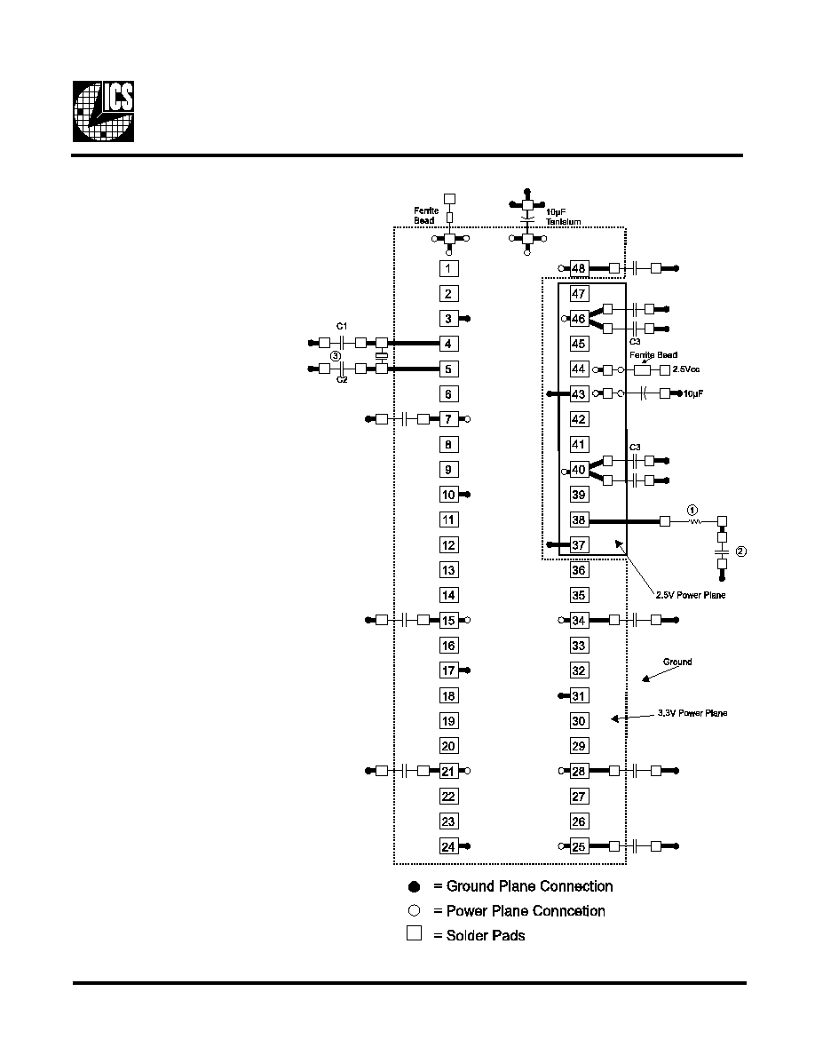
General Layout Precautions:
1) Use a ground plane on the top layer
of the PCB in all areas not used by
traces.
2) Make all power traces and vias as
wide as possible to lower inductance.
Notes:
1 All clock outputs should have series
terminating resistor. Not shown in all
places to improve readibility of
diagram
2 Optional EMI capacitor should be
used on all CPU, SDRAM, and PCI
outputs.
3 Optional crystal load capacitors are
recommended.
Capacitor Values:
C1, C2 : Crystal load values determined by user
C3 : 100pF ceramic
All unmarked capacitors are 0.01µF ceramic
16
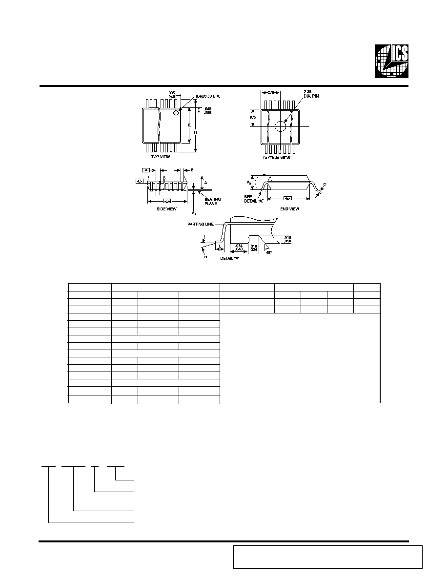
ICS9148-02
Ordering Information
ICS9148F-02
Pattern Number (2 or 3 digit number for parts with ROM code patterns)
Package Type
F=SSOP
Device Type (consists of 3 or 4 digit numbers)
Prefix
ICS, AV = Standard Device
Example:
ICS XXXX F - PPP
This table in inches
SSOP Package
L
O
B
M
Y
S
S
N
O
I
S
N
E
M
I
D
N
O
M
M
O
C
S
N
O
I
T
A
I
R
A
V
D
N
.
N
I
M
.
M
O
N
.
X
A
M
.
N
I
M
.
M
O
N
.
X
A
M
A
5
9
0
.
1
0
1
.
0
1
1
.
C
A
0
2
6
.
5
2
6
.
0
3
6
.
8
4
1
A
8
0
0
.
2
1
0
.
6
1
0
.
D
A
0
2
7
.
5
2
7
.
0
3
7
.
6
5
2
A
8
8
0
.
0
9
0
.
2
9
0
.
B
8
0
0
.
0
1
0
.
5
3
1
0
.
C
5
0
0
.
6
0
0
.
5
8
0
0
.
D
s
n
o
i
t
a
i
r
a
V
e
e
S
E
2
9
2
.
6
9
2
.
9
9
2
.
e
C
S
B
5
2
0
.
0
H
0
0
4
.
6
0
4
.
0
1
4
.
h
0
1
0
.
3
1
0
.
6
1
0
.
L
4
2
0
.
2
3
0
.
0
4
0
.
N
s
n
o
i
t
a
i
r
a
V
e
e
S
°
0
°
5
°
8
X
5
8
0
.
3
9
0
.
0
0
1
.
ICS reserves the right to make changes in the device data identified in this
publication without further notice. ICS advises its customers to obtain the latest
version of all device data to verify that any information being relied upon by the
customer is current and accurate.