Äîêóìåíòàöèÿ è îïèñàíèÿ www.docs.chipfind.ru
Integrated
Circuit
Systems, Inc.
General Description
Features
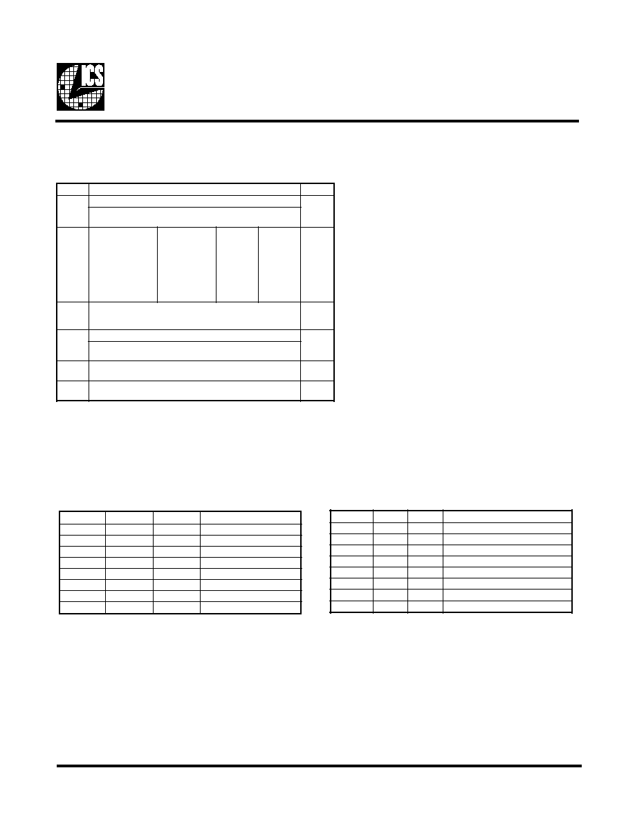
ICS9148- 36
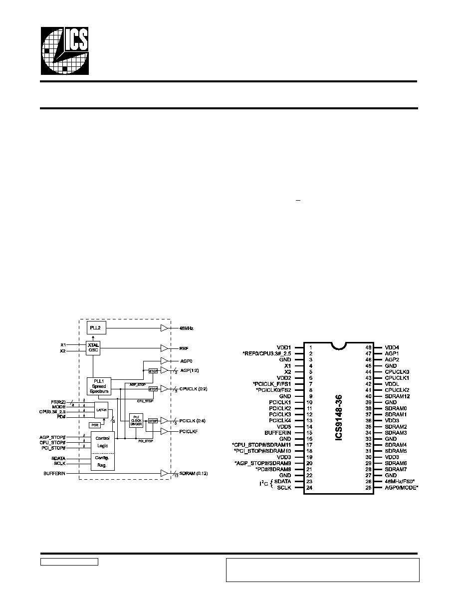
Block Diagram
Pentium is a trademark of Intel Corporation
I
2
C is a trademark of Philips Corporation
Frequency Generator & Integrated Buffers for PENTIUM/Pro
TM
9148-36 Rev I 11/11/99
Pin Configuration
48-Pin SSOP
Power Groups
VDD1 = REF (0:1), X1, X2
VDD2 = PCICLK_F, PCICLK(0:5)
VDD3 = SDRAM (0:12), supply for PLL core
VDD4 = AGP (1:2)
VDD5 = Fixed PLL, 48MHz , AGP0
VDDL = CPUCLK (0:2)
* Internal Pull-up Resistor of
240K to 3.3V on indicated inputs
The ICS9148-36 generates all clocks required for high speed
RISC or CISC microprocessor systems such as Intel PentiumPro
or Cyrix. Eight different reference frequency multiplying factors
are externally selectable with smooth frequency transitions.
Spread spectrum may be enabled through I2C programming.
Spread spectrum typically reduces system EMI by 8dB to
10dB. This simplifies EMI qualification without resorting to
board design iterations or costly shielding. The ICS9148-36
employs a proprietary closed loop design, which tightly
controls the percentage of spreading over process and
temperature variations.
Serial programming I
2
C interface allows changing functions,
stop clock programming and frequency selection. The
SDRAM12 output may be used as a feed back into an off chip
PLL.
Generates the following system clocks:
- 3 CPU(2.5V/3.3V) upto 100MHz.
- 6 PCI(3.3V) @ 33.3MHz
- 3AGP(3.3V) @ 2 x PCI
- 13 SDRAMs(3.3V) up to 100MHz
- 1 REF (3.3V) @ 14.318MHz
Skew characteristics:
- CPU CPU<250ps
- CPU(early) PCI : 1-4ns, Center 2-6ns
- AGP - PCI: 250ps
Supports Spread Spectrum modulation & I
2
C
programming for Power Management, Frequency Select
Efficient Power management scheme through PCI and
CPU STOP CLOCKS.
Uses external 14.318MHz crystal
48 pin 300mil SSOP.
ICS reserves the right to make changes in the device data identified in this
publication without further notice. ICS advises its customers to obtain the latest
version of all device data to verify that any information being relied upon by the
customer is current and accurate.
2
ICS9148-36
Pin Descriptions
Notes:
1:
Internal Pull-up Resistor of 240K to 3.3V on indicated inputs
2:
Bidirectional input/output pins, input logic levels are latched at internal power-on-reset. Use 10Kohm resistor to
program logic Hi to VDD or GND for logic low.
R
E
B
M
U
N
N
I
P
E
M
A
N
N
I
P
E
P
Y
T
N
O
I
T
P
I
R
C
S
E
D
1
1
D
D
V
R
W
P
V
3
.
3
l
a
n
i
m
o
n
,
y
l
p
p
u
s
r
e
w
o
p
L
A
T
X
,
)
2
:
0
(
f
e
R
2
0
F
E
R
T
U
O
.
k
c
o
l
c
e
c
n
e
r
e
f
e
r
z
h
M
8
1
3
.
4
1
5
.
2
_
#
3
.
3
U
P
C
2
,
1
N
I
V
3
.
3
=
W
O
L
,
U
P
C
V
5
.
2
=
h
g
i
H
.
V
5
.
2
r
o
V
3
.
3
s
i
2
L
D
D
V
r
e
h
t
e
h
w
s
e
t
a
c
i
d
n
I
U
P
C
1
t
u
p
n
i
d
e
h
c
t
a
L
.
2
,
7
2
,
2
2
,
6
1
,
9
,
3
5
4
,
9
3
,
3
3
D
N
G
R
W
P
d
n
u
o
r
G
4
1
X
N
I
k
c
a
b
d
e
e
f
d
n
a
)
F
p
3
3
(
p
a
c
d
a
o
l
l
a
n
r
e
t
n
i
s
a
h
,
t
u
p
n
i
l
a
t
s
y
r
C
2
X
m
o
r
f
r
o
t
s
i
s
e
r
5
2
X
T
U
O
d
a
o
l
l
a
n
r
e
t
n
i
s
a
H
.
z
H
M
8
1
3
.
4
1
y
l
l
a
n
i
m
o
n
,
t
u
p
t
u
o
l
a
t
s
y
r
C
)
F
p
3
3
(
p
a
c
6
2
D
D
V
R
W
P
V
3
.
3
l
a
n
i
m
o
n
,
)
5
:
0
(
K
L
C
I
C
P
d
n
a
F
_
K
L
C
I
C
P
r
o
f
y
l
p
p
u
S
7
F
_
K
L
C
I
C
P
T
U
O
w
e
k
s
s
n
4
-
1
h
t
i
w
s
K
L
C
U
P
C
h
t
i
w
s
u
o
n
o
r
h
c
n
y
S
.
t
u
p
t
u
o
k
c
o
l
c
I
C
P
g
n
i
n
n
u
r
e
e
r
F
#
P
O
T
S
_
I
C
P
y
b
d
e
t
c
e
f
f
a
t
o
n
s
i
s
i
h
T
)
y
l
r
a
e
U
P
C
(
1
S
F
2
,
1
N
I
e
h
t
s
n
i
m
r
e
t
e
d
s
n
i
p
S
F
r
e
h
t
o
h
t
i
w
g
n
o
l
A
.
t
u
p
n
I
d
e
h
c
t
a
L
.
n
i
p
t
c
e
l
e
s
y
c
n
e
u
q
e
r
F
.
s
e
i
c
n
e
u
w
e
r
f
P
G
A
&
I
C
P
,
M
A
R
D
S
,
U
P
C
8
0
K
L
C
I
C
P
T
U
O
)
y
l
r
a
e
U
P
C
(
w
e
k
s
s
n
4
-
1
h
t
i
w
s
K
L
C
U
P
C
s
u
o
n
u
o
r
h
c
n
y
S
.
s
t
u
p
t
u
o
k
c
o
l
c
I
C
P
2
S
F
2
,
1
N
I
t
u
p
n
I
d
e
h
c
t
a
L
.
n
i
p
t
c
e
l
e
s
y
c
n
e
u
q
e
r
F
3
1
,
2
1
,
1
1
,
0
1
)
4
:
1
(
K
L
C
I
C
P
T
U
O
)
y
l
r
a
e
U
P
C
(
w
e
k
s
s
n
4
-
1
h
t
i
w
s
K
L
C
U
P
C
s
u
o
n
u
o
r
h
c
n
y
S
.
s
t
u
p
t
u
o
k
c
o
l
c
I
C
P
4
1
5
D
D
V
R
W
P
0
P
G
A
,
z
H
M
8
4
,
L
L
P
d
e
x
i
f
r
o
f
y
l
p
p
u
S
5
1
N
I
R
E
F
F
U
B
N
I
.
s
r
e
f
f
u
b
M
A
R
D
S
r
o
f
n
i
p
t
u
p
n
I
7
1
#
P
O
T
S
_
U
P
C
1
N
I
e
l
i
b
o
M
n
i
(
w
o
l
t
u
p
n
i
n
e
h
w
,
l
e
v
e
l
0
c
i
g
o
l
t
a
s
k
c
o
l
c
)
3
:
0
(
K
L
C
U
P
C
s
t
l
a
H
)
0
=
E
D
O
M
,
e
d
o
M
1
1
M
A
R
D
S
T
U
O
t
u
p
t
u
o
k
c
o
l
c
M
A
R
D
S
8
1
#
P
O
T
S
_
I
C
P
1
N
I
,
e
d
o
m
e
l
i
b
o
m
n
I
(
w
o
l
t
u
p
n
i
n
e
h
w
,
l
e
v
e
l
0
c
i
g
o
l
t
a
s
k
c
o
l
c
)
5
:
0
(
K
L
C
I
C
P
s
t
l
a
H
)
0
=
E
D
O
M
0
1
M
A
R
D
S
T
U
O
t
u
p
t
u
o
k
c
o
l
c
M
A
R
D
S
,
4
3
,
2
3
,
1
3
,
9
2
,
8
2
8
3
,
7
3
,
5
3
)
9
:
0
(
M
A
R
D
S
T
U
O
.
s
t
u
p
t
u
o
k
c
o
l
c
M
A
R
D
S
0
2
#
P
O
T
S
_
P
G
A
N
I
t
u
p
n
i
n
e
h
w
l
e
v
e
l
"
0
"
c
i
g
o
l
t
a
s
k
c
o
l
c
)
2
:
1
(
P
G
A
s
t
l
a
h
t
u
p
n
i
s
u
o
n
o
r
h
c
n
y
s
a
s
i
h
T
0
P
G
A
t
c
e
f
f
a
t
o
n
s
e
o
D
)
0
=
E
D
O
M
,
e
d
o
M
e
l
i
b
o
M
n
i
(
w
o
l
9
M
A
R
D
S
T
U
O
t
u
p
t
u
o
k
c
o
l
c
M
A
R
D
S
1
2
#
D
P
N
I
l
a
n
r
e
t
n
i
&
l
a
t
s
y
r
c
,
O
C
V
e
h
t
s
p
o
t
S
t
u
p
n
i
n
w
o
D
r
e
w
o
P
s
u
o
n
o
r
e
h
c
n
y
s
a
s
i
h
T
)
0
=
E
D
O
M
,
e
d
o
M
e
l
i
b
o
M
n
I
(
.
w
o
L
,
e
v
i
t
c
a
n
e
h
w
s
k
c
o
l
c
8
M
A
R
D
S
T
U
O
t
u
p
t
u
o
k
c
o
l
c
M
A
R
D
S
6
3
,
0
3
,
9
1
3
D
D
V
R
W
P
,
s
k
c
o
l
c
z
H
M
8
4
,
e
r
o
C
U
P
C
,
)
1
1
:
0
(
M
A
R
D
S
r
o
f
y
l
p
p
u
S
.
V
3
.
3
l
a
n
i
m
o
n
3
2
A
T
A
D
S
N
I
I
r
o
f
t
u
p
n
i
a
t
a
D
2
.
t
u
p
n
i
l
a
i
r
e
s
C
4
2
K
L
C
S
N
I
I
f
o
t
u
p
n
i
k
c
o
l
C
2
t
u
p
n
i
C
5
2
0
P
G
A
T
U
O
y
b
d
e
t
c
e
f
f
a
t
o
N
.
4
D
D
V
y
b
d
e
r
e
w
o
p
,
t
u
p
t
u
o
t
r
o
P
c
i
h
p
a
r
G
d
e
c
n
a
v
d
A
#
P
O
T
S
_
P
G
A
E
D
O
M
2
,
1
N
I
.
e
d
o
M
e
l
i
b
o
M
=
0
,
e
d
o
M
p
o
t
k
s
e
D
=
1
,
n
i
p
t
c
e
l
e
s
n
o
i
t
c
n
u
f
1
2
&
0
2
,
8
1
,
7
1
n
i
P
.
t
u
p
n
I
d
e
h
c
t
a
L
6
2
z
H
M
8
4
T
U
O
.
g
n
i
m
i
t
B
S
U
r
o
f
k
c
o
l
c
t
u
p
t
u
o
z
H
M
8
4
0
S
F
2
,
1
N
I
e
h
t
s
n
i
m
r
e
t
e
d
s
n
i
p
S
F
r
e
h
t
o
h
t
i
w
g
n
o
l
A
.
t
u
p
n
I
d
e
h
c
t
a
L
.
n
i
p
t
c
e
l
e
s
y
c
n
e
u
q
e
r
F
.
s
e
i
c
n
e
u
w
e
r
f
P
G
A
&
I
C
P
,
M
A
R
D
S
,
U
P
C
4
4
,
3
4
,
1
4
)
3
:
0
(
K
L
C
U
P
C
T
U
O
w
o
L
=
#
P
O
T
S
_
U
P
C
f
i
w
o
L
.
2
L
D
D
V
y
b
d
e
r
e
w
o
p
,
s
t
u
p
t
u
o
k
c
o
l
c
U
P
C
0
4
2
1
M
A
R
D
S
T
U
O
.
t
u
p
t
u
o
k
c
o
l
c
M
A
R
D
S
k
c
a
b
d
e
e
F
2
4
L
D
D
V
R
W
P
l
a
n
i
m
o
n
V
3
.
3
r
o
V
5
.
2
r
e
h
t
i
e
,
)
3
:
0
(
U
P
C
r
o
f
y
l
p
p
u
S
7
4
,
6
4
)
2
:
1
(
P
G
A
T
U
O
.
4
D
D
V
y
b
d
e
r
e
w
o
p
,
s
t
u
p
t
u
o
t
r
o
P
c
i
h
p
a
r
G
d
e
c
n
a
v
d
A
8
4
4
D
D
V
R
W
P
)
2
:
0
(
P
G
A
r
o
f
y
l
p
p
u
S
3
ICS9148-36
Functionality
V
DD
1, 2, 3, 4 = 3.3V±5%, V
DDL
= 2.5V ±5% or 3.3 ±5%, TA= 0 to 70°C
Crystal (X1, X2) = 14.31818MHz
5
.
2
_
#
3
.
3
U
P
C
l
e
v
e
l
t
u
p
n
I
)
a
t
a
D
d
e
h
c
t
a
L
(
r
o
f
d
e
t
c
e
l
e
S
r
e
f
f
u
B
:
t
a
n
o
i
t
a
r
e
p
o
1
D
D
V
V
5
.
2
0
D
D
V
V
3
.
3
CPU 3.3#_2.5V Buffer selector for CPUCLK drivers.
Power Management Functionality
Mode Pin - Power Management Input Control
5
2
n
i
P
,
E
D
O
M
)
t
u
p
n
I
d
e
h
c
t
a
L
(
7
1
n
i
P
8
1
n
i
P
0
2
n
i
P
1
2
n
i
P
0
#
P
O
T
S
_
U
P
C
)
T
U
P
N
I
(
#
P
O
T
S
_
I
C
P
)
T
U
P
N
I
(
#
P
O
T
S
_
P
G
A
)
T
U
P
N
I
(
#
D
P
)
T
U
P
N
I
(
1
1
1
M
A
R
D
S
)
T
U
P
T
U
O
(
0
1
M
A
R
D
S
)
T
U
P
T
U
O
(
9
M
A
R
D
S
)
T
U
P
T
U
O
(
8
M
A
R
D
S
)
T
U
P
T
U
O
(
#
P
O
T
S
_
P
G
A
#
P
O
T
S
_
U
P
C
#
P
O
T
S
_
I
C
P
,
P
G
A
K
L
C
U
P
C
s
t
u
p
t
u
O
K
L
C
I
C
P
)
5
:
0
(
,
F
_
K
L
C
I
C
P
z
H
M
8
4
,
F
E
R
M
A
R
D
S
d
n
a
l
a
t
s
y
r
C
C
S
O
O
C
V
)
2
:
1
(
P
G
A
1
0
1
w
o
L
d
e
p
p
o
t
S
g
n
i
n
n
u
R
g
n
i
n
n
u
R
g
n
i
n
n
u
R
g
n
i
n
n
u
R
g
n
i
n
n
u
R
1
1
1
g
n
i
n
n
u
R
g
n
i
n
n
u
R
g
n
i
n
n
u
R
g
n
i
n
n
u
R
g
n
i
n
n
u
R
g
n
i
n
n
u
R
1
1
0
g
n
i
n
n
u
R
w
o
L
d
e
p
p
o
t
S
g
n
i
n
n
u
R
g
n
i
n
n
u
R
g
n
i
n
n
u
R
g
n
i
n
n
u
R
0
1
1
g
n
i
n
n
u
R
g
n
i
n
n
u
R
g
n
i
n
n
u
R
g
n
i
n
n
u
R
g
n
i
n
n
u
R
w
o
L
d
e
p
p
o
t
S
2
S
F
1
S
F
0
S
F
M
A
R
D
S
,
U
P
C
)
z
H
M
(
I
C
P
)
z
H
M
(
P
G
A
)
z
H
M
(
C
I
P
A
O
I
,
F
E
R
)
z
H
M
(
1
1
1
0
0
1
3
.
3
3
6
.
6
6
8
1
3
.
4
1
1
1
0
5
2
.
5
9
5
7
.
1
3
5
.
3
6
8
1
3
.
4
1
1
0
1
3
.
3
8
3
.
3
3
6
.
6
6
8
1
3
.
4
1
1
0
0
5
7
0
3
0
6
8
1
3
.
4
1
0
1
1
5
7
5
.
7
3
5
7
8
1
3
.
4
1
0
1
0
5
.
8
6
5
2
.
4
3
5
.
8
6
8
1
3
.
4
1
0
0
1
8
.
6
6
4
.
3
3
8
.
6
6
8
1
3
.
4
1
0
0
0
0
6
0
3
0
6
8
1
3
.
4
1
4
ICS9148-36
1.
The ICS clock generator is a slave/receiver, I
2
C component. It can read back the data stored in the latches for verification.
Read-Back will support Intel PIIX4 "Block-Read" protocol.
2.
The data transfer rate supported by this clock generator is 100K bits/sec or less (standard mode)
3.
The input is operating at 3.3V logic levels.
4.
The data byte format is 8 bit bytes.
5.
To simplify the clock generator I
2
C interface, the protocol is set to use only "Block-Writes" from the controller. The
bytes must be accessed in sequential order from lowest to highest byte with the ability to stop after any complete byte
has been transferred. The Command code and Byte count shown above must be sent, but the data is ignored for those
two bytes. The data is loaded until a Stop sequence is issued.
6.
At power-on, all registers are set to a default condition, as shown.
General I
2
C serial interface information
The information in this section assumes familiarity with I
2
C programming.
For more information, contact ICS for an I
2
C programming application note.
How to Write:
Controller (host) sends a start bit.
Controller (host) sends the write address D2
(H)
ICS clock will acknowledge
Controller (host) sends a dummy command code
ICS clock will acknowledge
Controller (host) sends a dummy byte count
ICS clock will acknowledge
Controller (host) starts sending first byte (Byte 0)
through byte 5
ICS clock will acknowledge each byte one at a time.
Controller (host) sends a Stop bit
How to Read:
Controller (host) will send start bit.
Controler (host) sends the read address D3
(H)
ICS clock will acknowledge
ICS clock will send the byte count
Controller (host) acknowledges
ICS clock sends first byte (Byte 0) through byte 5
Controller (host) will need to acknowledge each byte
Controller (host) will send a stop bit
Notes:
Controller (Host)
ICS (Slave/Receiver)
Start Bit
Address
D3
(H)
ACK
Byte Count
ACK
Byte 0
ACK
Byte 1
ACK
Byte 2
ACK
Byte 3
ACK
Byte 4
ACK
Byte 5
ACK
Stop Bit
How to Read:
Controller (Host)
ICS (Slave/Receiver)
Start Bit
Address
D2
(H)
ACK
Dummy Command Code
ACK
Dummy Byte Count
ACK
Byte 0
ACK
Byte 1
ACK
Byte 2
ACK
Byte 3
ACK
Byte 4
ACK
Byte 5
ACK
Stop Bit
How to Write:
5
ICS9148-36
Byte0: Functionality and Frequency Select Register (default = 0)
Serial Configuration Command Bitmap
I
2
C is a trademark of Philips Corporation
Note 1. Default at Power-up will be for latched logic inputs
to define frequency. Bits 4, 5, 6 are default to 000,
and if bit 3 is written to a 1 to use Bits 6:4, then
these should be defined to desired frequency at same
write cycle.
Note: PWD = Power-Up Default
t
i
B
n
o
i
t
p
i
r
c
s
e
D
D
W
P
7
t
i
B
n
o
i
t
a
r
e
p
o
l
a
m
r
o
n
r
o
f
0
e
b
t
s
u
M
0
n
o
i
t
a
l
u
d
o
M
m
u
r
t
c
e
p
S
d
a
e
r
p
S
%
5
2
.
0
±
-
0
n
o
i
t
a
l
u
d
o
M
m
u
r
t
c
e
p
S
d
a
e
r
p
S
%
6
.
0
±
-
1
t
i
B
4
:
6
4
t
i
B
5
t
i
B
6
t
i
B
1
1
1
0
1
1
1
0
1
0
0
1
1
1
0
0
1
0
1
0
0
0
0
0
k
c
o
l
C
U
P
C
0
0
1
5
2
.
5
9
3
.
3
8
5
7
5
7
5
.
8
6
8
.
6
6
0
6
I
C
P
3
.
3
3
5
7
.
1
3
3
.
3
3
0
3
5
.
7
3
5
2
.
4
3
4
.
3
3
0
3
P
G
A
6
.
6
6
5
.
3
6
6
.
6
6
0
6
5
7
5
.
8
6
8
.
6
6
0
6
1
e
t
o
N
3
t
i
B
,
t
c
e
l
e
s
e
r
a
w
d
r
a
h
y
b
d
e
t
c
e
l
e
s
s
i
y
c
n
e
u
q
e
r
F
-
0
s
t
u
p
n
I
d
e
h
c
t
a
L
)
e
v
o
b
a
(
4
:
6
t
i
B
y
b
d
e
t
c
e
l
e
s
s
i
y
c
n
e
u
q
e
r
F
-
1
0
2
t
i
B
n
o
i
t
a
r
e
p
o
l
a
m
r
o
n
r
o
f
0
e
b
t
s
u
M
0
.
e
p
y
t
d
a
e
r
p
s
r
e
t
n
e
c
m
u
r
t
c
e
p
S
d
a
e
r
p
S
-
0
.
e
p
y
t
d
a
e
r
p
s
n
w
o
d
m
u
r
t
c
e
p
S
d
a
e
r
p
S
-
1
1
t
i
B
l
a
m
r
o
N
-
0
d
e
l
b
a
n
E
m
u
r
t
c
e
p
S
d
a
e
r
p
S
-
1
0
0
t
i
B
g
n
i
n
n
u
R
-
0
s
t
u
p
t
u
o
l
l
a
e
t
a
t
s
i
r
T
-
1
0
Byte 1: CPU, Active/Inactive Register
(1 = enable, 0 = disable)
Notes:
1. Inactive means outputs are held LOW and are disabled
from switching.
Notes:
1. Inactive means outputs are held LOW and are disabled
from switching.
t
i
B
#
n
i
P
D
W
P
n
o
i
t
p
i
r
c
s
e
D
7
t
i
B
-
1
)
d
e
v
r
e
s
e
R
(
6
t
i
B
-
X
#
2
S
F
5
t
i
B
-
X
#
1
S
F
4
t
i
B
0
4
1
)
t
c
a
n
I
/
t
c
A
(
2
1
M
A
R
D
S
3
t
i
B
-
1
)
d
e
v
r
e
s
e
R
(
2
t
i
B
1
4
1
)
t
c
a
n
I
/
t
c
A
(
2
K
L
C
U
P
C
1
t
i
B
3
4
1
)
t
c
a
n
I
/
t
c
A
(
1
K
L
C
U
P
C
0
t
i
B
4
4
1
)
t
c
a
n
I
/
t
c
A
(
0
K
L
C
U
P
C
t
i
B
#
n
i
P
D
W
P
n
o
i
t
p
i
r
c
s
e
D
7
t
i
B
-
X
5
.
2
_
#
3
.
3
U
P
C
6
t
i
B
7
1
)
t
c
a
n
I
/
t
c
A
(
F
_
K
L
C
I
C
P
5
t
i
B
-
X
#
0
S
F
4
t
i
B
3
1
1
)
t
c
a
n
I
/
t
c
A
(
4
K
L
C
I
C
P
3
t
i
B
2
1
1
)
t
c
a
n
I
/
t
c
A
(
3
K
L
C
I
C
P
2
t
i
B
1
1
1
)
t
c
a
n
I
/
t
c
A
(
2
K
L
C
I
C
P
1
t
i
B
0
1
1
)
t
c
a
n
I
/
t
c
A
(
1
K
L
C
I
C
P
0
t
i
B
8
1
)
t
c
a
n
I
/
t
c
A
(
0
K
L
C
I
C
P
Byte 2: PCI Active/Inactive Register
(1 = enable, 0 = disable)