Äîêóìåíòàöèÿ è îïèñàíèÿ www.docs.chipfind.ru
Integrated
Circuit
Systems, Inc.
General Description
Features
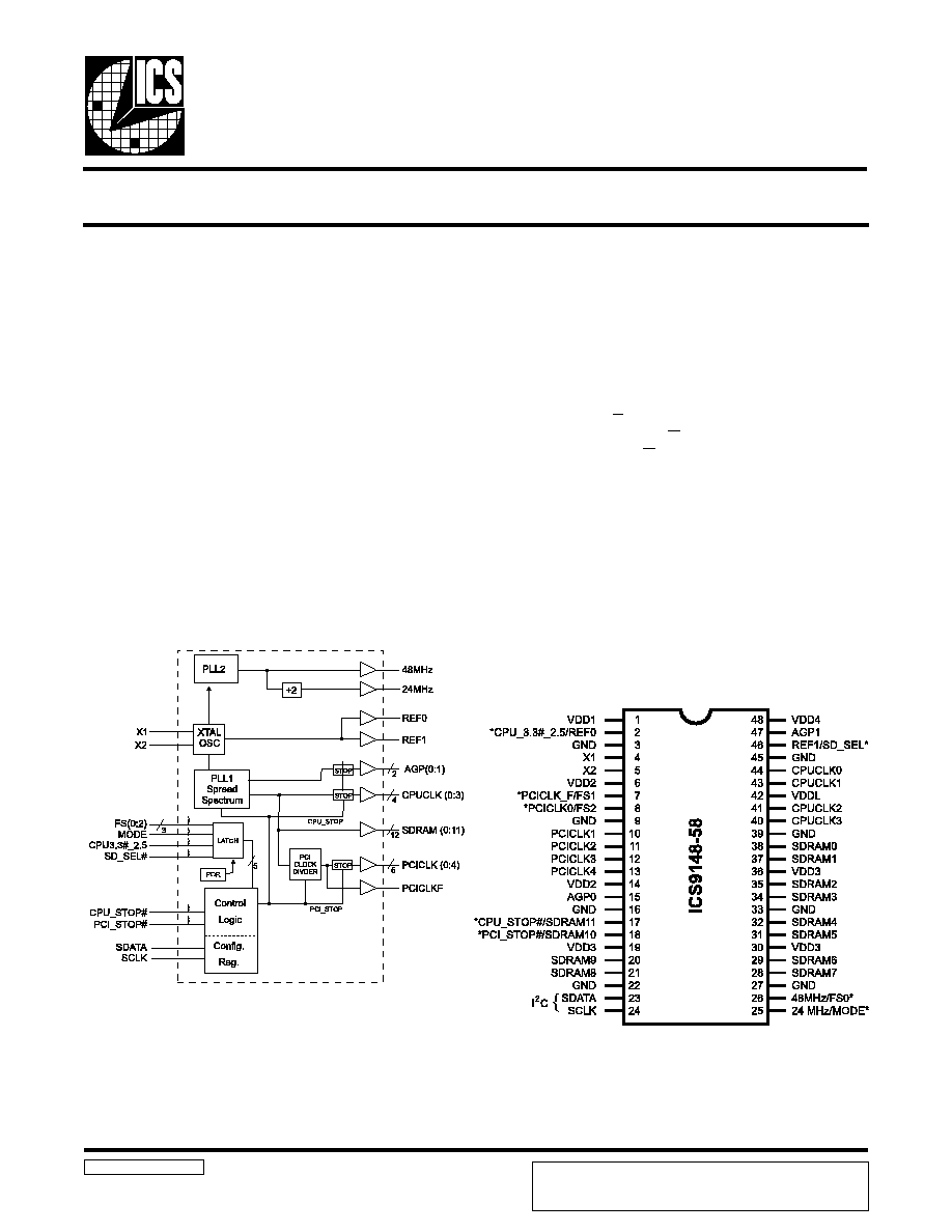
ICS9148-58
Block Diagram
Pentium is a trademark of Intel Corporation
I
2
C is a trademark of Philips Corporation
Frequency Generator & Integrated Buffers for PENTIUM/Pro
TM
9148-58 Rev C 12/07/98
Pin Configuration
Generates the following system clocks:
- 4 CPU(2.5V/3.3V) upto 100MHz.
- 6 PCI(3.3V) @ 33.3MHz
- 2AGP(3.3V) @ 2 x PCI
- 12 SDRAMs(3.3V) @ either CPU or AGP
- 2 REF (3.3V) @ 14.318MHz
Skew characteristics:
- CPU CPU<250ps
- SDRAM SDRAM < 250ps
- CPU SDRAM < 250ps
- CPU(early) PCI : 1-4ns
Spread Spectrum 0 to -5% down spread.
Serial I
2
C interface for Power Management, Frequency
Select, Spread Spectrum.
Efficient Power management scheme through PCI and CPU
STOP CLOCKS.
Uses external 14.318MHz crystal
48 pin 300mil SSOP.
48-Pin SSOP
Power Groups
VDD1 = REF (0:1), X1, X2
VDD2 = PCICLK_F, PCICLK(0:5)
VDD3 = SDRAM (0:11), supply for PLL core,
24 MHz, 48MHz
VDD4 = AGP (0:1)
VDDL = CPUCLK (0:3)
* Internal Pull-up Resistor of
240K to 3.3V on indicated inputs
The ICS9148-58 is the single chip clock solution for Desktop/
Notebook designs using the VIA MVP3 style chipset. It
provides all necessary clock signals for such a system.
Spread spectrum may be enabled through I2C programming.
Spread spectrum typically reduces system EMI by 8dB to
10dB. This simplifies EMI qualification without resorting to
board design iterations or costly shielding. The ICS9148-58
employs a proprietary closed loop design, which tightly
controls the percentage of spreading over process and
temperature variations.
Serial programming I
2
C interface allows changing functions,
stop clock programming and frequency selection. The SD_SEL
latched input allows the SDRAM frequency to follow the
CPUCLK frequency(SD_SEL=1) or the AGP clock
frequency(SD_SEL=0)
ICS reserves the right to make changes in the device data identified in
this publication without further notice. ICS advises its customers to
obtain the latest version of all device data to verify that any
information being relied upon by the customer is current and accurate.
2
ICS9148- 58
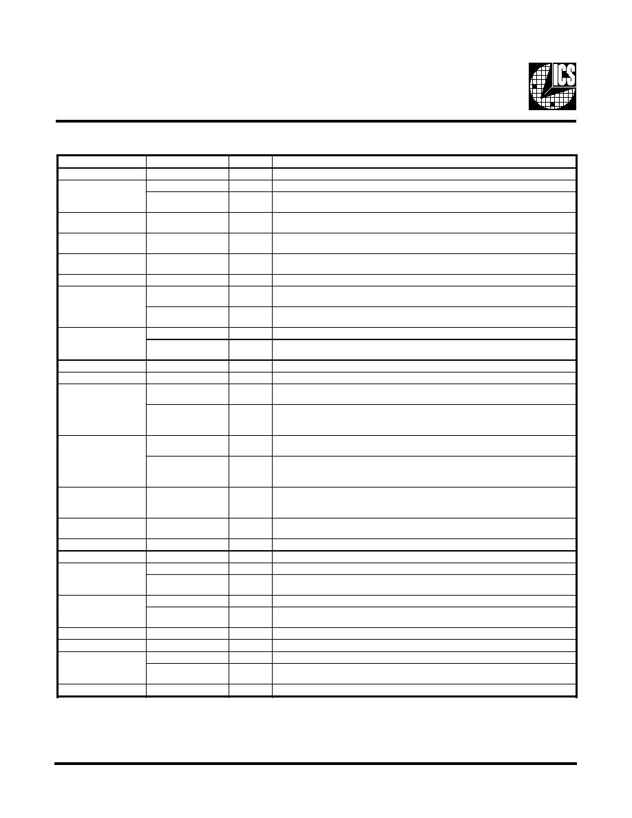
Pin Descriptions
Notes:
1:
Internal Pull-up Resistor of 240K to 3.3V on indicated inputs
2:
Bidirectional input/output pins, input logic levels are latched at internal power-on-reset. Use 10Kohm resistor to
program logic Hi to VDD or GND for logic low.
PIN NUMBER
PIN NAME
TYPE
DESCRIPTION
1
VDD1
PWR
Ref (0:2), XTAL power supply, nominal 3.3V
2
REF0
OUT
14.318 MHz reference clock.
CPU3.3#_2.5
1,2
IN
Indicates whether VDDL2 is 3.3V or 2.5V. High=2.5V CPU, LOW=3.3V
CPU
1
. Latched input
2
3,9,16,22,27,
33,39,45
GND
PWR
Ground
4
X1
IN
Crystal input, has internal load cap (33pF) and feedback
resistor from X2
5
X2
OUT
Crystal output, nominally 14.318MHz. Has internal load
cap (33pF)
6,14
VDD2
PWR
Supply for PCICLK_F and PCICLK (0:5), nominal 3.3V
7
PCICLK_F
OUT
Free running PCI clock output. Synchrounous with CPUCLKs with 1-4ns
skew (CPU early) This is not affected by PCI_STOP#
FS1
1, 2
IN
Frequency select pin. Latched Input. Along with other FS pins determins the
CPU, SDRAM, PCI & AGP frequencies.
8
PCICLK0
OUT
PCI clock output. Synchrounous CPUCLKs with 1-4ns skew (CPU early)
FS2
1, 2
IN
Frequency select pin. Latched Input Along with other FS pins determins the
CPU, SDRAM, PCI & AGP frequencies.
10, 11, 12, 13
PCICLK(1:4)
OUT
PCI clock outputs. Synchrounous CPUCLKs with 1-4ns skew (CPU early)
15, 47
AGP (0:1)
OUT
Advanced Graphic Port outputs, powered by VDD4.
17
CPU_STOP#
1
IN
This asyncheronous input halts CPUCLK (0:3) and AGP (0:1) clocks at
logic 0 level, when input low (in Mobile Mode, MODE=0)
SDRAM 11
OUT
SDRAM clock output. Frequency is selected by the SD_SEL latched input.
SD_SEL = 1 at power on causes SDRAM frequency = CPU frenquencies
SD_SEL = 0 at power on causes SDRAM frequencies = AGP frequencies
18
PCI_STOP#
1
IN
This asyncheronous input halts PCICLK(0:5) clocks at logic 0 level, when
input low (In mobile mode, MODE=0)
SDRAM 10
OUT
SDRAM clock output. Frequency is selected by the SD_SEL latched input.
SD_SEL = 1 at power on causes SDRAM frequency = CPU frenquencies
SD_SEL = 0 at power on causes SDRAM frequencies = AGP frequencies
20, 21,28, 29, 31,
32, 34, 35,37,38
SDRAM (0:9)
OUT
SDRAM clock outputs. Frequency is selected by the SD_SEL latched input.
SD_SEL = 1 at power on causes SDRAM frequency = CPU frenquencies
SD_SEL = 0 at power on causes SDRAM frequencies = AGP frequencies
19,30,36
VDD3
PWR
Supply for SDRAM (0:11), CPU Core and 24, 48MHz clocks,
nominal 3.3V.
23
SDATA
IN
Data input for I
2
C serial input.
24
SCLK
IN
Clock input of I
2
C input
25
24MHz
OUT
24MHz output clock, for Super I/O timing.
MODE
1, 2
IN
Pin 17, pin 18 function select pin, 1=Desktop Mode, 0=Mobile Mode.
Latched Input.
26
48MHz
OUT
48MHz output clock, for USB timing.
FS0
1, 2
IN
Frequency select pin. Latched Input Along with other FS pins determins the
CPU, SDRAM, PCI & AGP frequencies.
40, 41, 43, 44
CPUCLK(0:3)
OUT
CPU clock outputs, powered by VDDL2. Low if CPU_STOP#=Low
42
VDDL
PWR
Supply for CPU (0:3), either 2.5V or 3.3V nominal
46
REF1
OUT
14.318MHz reference clock.
SD_SEL
IN
Latched input at Power On selects either CPU (SDSEL=1) or AGP
(SD_SEL=0) frequencies for the SDRAM clock outputs.
48
VDD4
PWR
Supply for AGP (0:1)
3
ICS9148-58
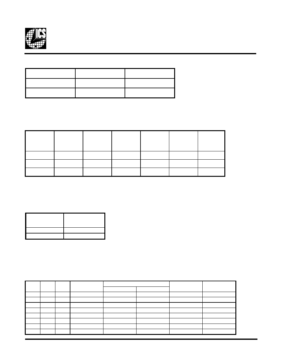
Functionality
V
DD
1, 2, 3, 4 = 3.3V±5%, V
DDL
= 2.5V ±5% or 3.3 ±5%, TA= 0 to 70°C
Crystal (X1, X2) = 14.31818MHz
CPU3.3#_2.5
Input level
(Latched Data)
Buffer Selected for
operation at:
1
2.5V VDD
0
3.3V VDD
CPU 3.3#_2.5V Buffer selector for CPUCLK drivers.
Power Management Functionality
Mode Pin - Power Management Input Control
MODE, Pin 25
(Latched Input)
Pin 17
Pin 18
0
CPU_STOP#
(INPUT)
PCI_STOP#
(INPUT)
1
SDRAM 11
(OUTPUT)
SDRAM 10
(OUTPUT)
CPU_STOP#
PCI_STOP#
AGP,
CPUCLK
Outputs
PCICLK
(0:5)
PCICLK_F,
REF,
24/48MHz
and SDRAM
Crystal
OSC
VCO
0
1
Stopped Low
Running
Running
Running
Running
1
1
Running
Running
Running
Running
Running
1
0
Running
Stopped Low
Running
Running
Running
F S 2
F S 1
F S 0
C P U
(M H z)
S D R A M ( M H z)
P C I (M H z)
A G P ( M H z)
S D _ S E L = 1
S D _ S E L = 0
1
1
1
1 0 0 . 2
1 0 0 . 2
66.6
33.3
6 6 . 6
1
1
0
9 5 . 2 5
9 5 . 2 5
63.5
31.75
6 3 . 5
1
0
1
8 3 . 3
8 3 . 3
66.6
33.3
6 6 . 6
1
0
0
1 3 3 . 3
1 3 3 . 3
88.7
44.3
8 8 . 7
0
1
1
7 5
7 5
75
37.5
7 5
0
1
0
1 2 4
1 2 4
82.7
41.3
8 2 . 7
0
0
1
6 6 . 8
6 6 . 8
66.8
33.4
6 6 . 8
0
0
0
11 2
11 2
74.7
37.3
7 4 . 7
4
ICS9148- 58
Byte0: Functionality and Frequency Select Register
(default = 0)
Serial Configuration Command Bitmap
Bit
Description
PWD
Bit 7 Reserved
0
Bit
6:4
Bit6 Bit5
Bit4
111
110
101
100
011
010
001
000
CPU Clock
100.2
95.25
83.3
133.3
75
124
66.8
112
PCI
33.3
31.75
33.3
44.3
37.5
41.3
33.4
37.3
AGP
66.6
63.5
66.6
88.7
75
82.7
66.8
74.7
Note
1
Bit 3
0 - Frequency is selected by hardware select,
Latched Inputs
1 - Frequency is selected by Bit 6:4 (above)
0
Bit 2
0 - Spread Spectrum center spread type. ±.25%
1 - Spread Spectrum down spread type. 0 to -.5%
0
Bit 1 0 - Normal
1 - Spread Spectrum Enabled
0
Bit 0
0 - Running
1- Tristate all outputs
0
General I
2
C serial interface information
The information in this section assumes familiarity with I
2
C programming. For more information, contact ICS for an I
2
C
programming application note.
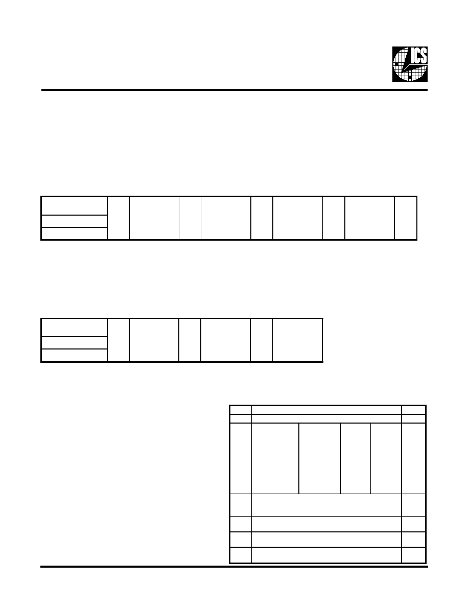
How to Write:
Send the address D2
(H)
.
Send two additional dummy bytes, a command code
and byte count.
Send the desired number of data bytes.
See the diagram below:
Note that the acknowledge bit is sent by the clock chip, and pulls the data line low. There is no minimum of data bytes that must
be sent.
How to Read:
Send the address D3
(H)
.
Send the byte count in binary coded decimal
Read back the desired number of data bytes
See the diagram below:
The following specifications should be observed:
1.
Operating voltage for I
2
C pins is 3.3V
2.
Maximum data transfer rate (SCLK) is 100K bits/sec.
Clock Generator
Address (7 bits)
ACK
+ 8 bits
dummy
command code
ACK
+ 8 bits
dummy Byte
count
ACK
Data Byte
1
ACK
Data Byte
N
ACK
A(6:0) & R/W#
D2
(H)
Clock Generator
Address (7 bits)
ACK
Byte
C ount
ACK
Data Byte
1
AC K
Data Byte
N
A(6:0) & R/W#
D3
(H)
I
2
C is a trademark of Philips Corporation
Note 1. Default at Power-up will be for latched logic inputs
to define frequency. Bits 4, 5, 6 are default to 000,
and if bit 3 is written to a 1 to use Bits 6:4, then
these should be defined to desired frequency at same
write cycle.
Note: PWD = Power-Up Default
5
ICS9148-58
Byte 1: CPU, Active/Inactive Register
(1 = enable, 0 = disable)
Byte 2: PCI Active/Inactive Register
(1 = enable, 0 = disable)
Byte 3: SDRAM Active/Inactive Register
(1 = enable, 0 = disable)
Notes:
1. Inactive means outputs are held LOW and are disabled
from switching.
Notes:
1. Inactive means outputs are held LOW and are disabled
from switching.
Notes:
1. Inactive means outputs are held LOW and are disabled
from switching.
Bit
Pin #
PWD
Description
Bit 7
-
1
(Reserved)
Bit 6
-
1
(Reserved)
Bit 5
-
1
(Reserved)
Bit 4
-
1
(Reserved)
Bit 3
40
1
CPUCLK3 (Act/Inact)
Bit 2
41
1
CPUCLK2 (Act/Inact)
Bit 1
43
1
CPUCLK1 (Act/Inact)
Bit 0
44
1
CPUCLK0 (Act/Inact)
Bit
Pin #
PWD
Description
Bit 7
-
1
(Reserved)
Bit 6
7
1
PCICLK_F (Act/Inact)
Bit 5
15
1
AGP0 (Act/Inact)
Bit 4
14
1
PCICLK4 (Act/Inact)
Bit 3
12
1
PCICLK3 (Act/Inact)
Bit 2
11
1
PCICLK2 (Act/Inact)
Bit 1
10
1
PCICLK1 (Act/Inact)
Bit 0
8
1
PCICLK0(Act/Inact)
Bit
Pin #
PWD
Description
Bit 7
28
1
SDRAM7 (Act/Inact)
Bit 6
29
1
SDRAM6 (Act/Inact)
Bit 5
31
1
SDRAM5 (Act/Inact)
Bit 4
32
1
SDRAM4 (Act/Inact)
Bit 3
34
1
SDRAM3 (Act/Inact)
Bit 2
35
1
SDRAM2 (Act/Inact)
Bit 1
37
1
SDRAM1 (Act/Inact)
Bit 0
38
1
SDRAM0 (Act/Inact)
Byte 4: SDRAM Active/Inactive Register
(1 = enable, 0 = disable)
Byte 5: Peripheral Active/Inactive Register
(1 = enable, 0 = disable)
Notes:
1. Inactive means outputs are held LOW and are disabled
from switching.
Notes:
1. Inactive means outputs are held LOW and are disabled
from switching.
Bit
Pin #
PWD
Description
Bit 7
-
1
(Reserved)
Bit 6
-
1
(Reserved)
Bit 5
-
1
(Reserved)
Bit 4
-
1
(Reserved)
Bit 3
17
1
SDRAM11 (Act/Inact)
(Desktop Mode Only)
Bit 2
18
1
SDRAM10 (Act/Inact)
(Desktop Mode Only)
Bit 1
20
1
SDRAM9 (Act/Inact)
Bit 0
21
1
SDRAM8 (Act/Inact)
Bit
Pin #
PWD
Description
Bit 7
-
1
(Reserved)
Bit 6
-
1
(Reserved)
Bit 5
-
1
(Reserved)
Bit 4
47
1
AGP1(Act/Inact)
Bit 3
-
1
(Reserved)
Bit 2
-
1
(Reserved)
Bit 1
46
1
REF1 (Act/Inact)
Bit 0
2
1
REF0 (Act/Inact)